Original Link: https://www.anandtech.com/show/16959/intel-innovation-alder-lake-november-4th
Intel 12th Gen Core Alder Lake for Desktops: Top SKUs Only, Coming November 4th
by Dr. Ian Cutress on October 27, 2021 12:00 PM EST- Posted in
- CPUs
- Intel
- DDR4
- DDR5
- PCIe 5.0
- Alder Lake
- Intel 7
- 12th Gen Core
- Z690
Over the past few months, Intel has been drip-feeding information about its next-generation processor family. Alder Lake, commercially known as Intel’s 12th Generation Core architecture, is officially being announced today for a November 4th launch. Alder Lake contains Intel’s latest generation high-performance cores combined with new high-efficiency cores for a new hybrid design, along with updates to Windows 11 to improve performance with the new heterogeneous layout. Only the six high-performance K and KF processor variants are coming this side of the New Year, with the rest due for Q1. We have specifications, details, and insights ahead of the product reviews on November 4th.
Today’s announcement also coincides with Intel’s InnovatiON virtual event happening today and tomorrow. This event is, as described in a number of press releases, a mini-Intel Developer Forum (IDF) event designed to emulate a small part of the highly prized annual conference that the company culled in 2017. As part of the event, there are 60+ sessions designed to cover new technology such as AI, networking, custom silicon, programming technologies/challenges, and introduce developers to more of Intel’s ecosystem. It includes a day one keynote from CEO Pat Gelsinger and other executives to share the new hardware announcements, and a day two keynote from CTO Greg Lavender on the software side. The goal was for this event to be in-person, which is usually where the most value came from the old IDF event, however this is the first attempt to revive the format.
Six Alder Lake CPUs, $589 For Core i9
The first things we’ll go into are the new CPUs that Intel is announcing today: the overclockable models of Intel 12th Gen Core. As with previous launches, we have Core i9, Core i7, and Core i5, with the key highlights including new support for DDR5, PCIe Gen 5, new overclocking features, and a change in how Intel is promoting its Thermal Design Power (TDP).
This is the table:
| Intel 12th Gen Core, Alder Lake | |||||||||
| AnandTech | Cores P+E/T |
E-Core Base |
E-Core Turbo |
P-Core Base |
P-Core Turbo |
IGP | Base W |
Turbo W |
Price $1ku |
| i9-12900K | 8+8/24 | 2400 | 3900 | 3200 | 5200 | 770 | 125 | 241 | $589 |
| i9-12900KF | 8+8/24 | 2400 | 3900 | 3200 | 5200 | - | 125 | 241 | $564 |
| i7-12700K | 8+4/20 | 2700 | 3800 | 3600 | 5000 | 770 | 125 | 190 | $409 |
| i7-12700KF | 8+4/20 | 2700 | 3800 | 3600 | 5000 | - | 125 | 190 | $384 |
| i5-12600K | 6+4/16 | 2800 | 3600 | 3700 | 4900 | 770 | 125 | 150 | $289 |
| i5-12600KF | 6+4/16 | 2800 | 3600 | 3700 | 4900 | - | 125 | 150 | $264 |
Each processor has a number of performance cores (P-cores) and efficiency cores (E-cores). The P-cores have SMT, whereas the E-cores do not, so we’re dealing with non-standard numbers of total threads. Inside the system, the P-core threads, E-core threads, and SMT threads are categorized for performance and efficiency, which we’ll get to later in the article. But with a new hybrid design also comes with new ways to showcase frequencies, and each set of cores will have its own base frequency and turbo frequency. The way power is marketed and used has also changed, designed to be clearer.
All processors will come with 16 lanes of PCIe 5.0 from the processor, and an additional 4 lanes of PCIe 4.0 for storage. Memory support is listed as both DDR5-4800 and DDR4-3200, although systems will only support one or the other, for a maximum of 128 GB. The K processors also feature 32 EUs of Intel’s Xe-LP graphics, designated as UHD Graphics 770. Prices will start at $264 for the base Core i5 model, up to $589 for the top Core i9 model.
Core i9-12900K/KF
For the Core i9-12900K, if we work from the ground up, the E-cores have a base frequency of 2.4 GHz but will turbo up to 3.9 GHz; the P-cores have a base frequency of 3.2 GHz, and an all-core turbo of 5.1 GHz. The P-cores that are considered the best (aka favored cores) will turbo up to 5.2 GHz.
With all the cores active, the system has all 30 MiB of L3 cache available. Intel lists the base power as 125 W, with a turbo power of 241 W. The 1000-unit price for the K model is $589, and the KF model without integrated graphics as $564. As these are 1000-unit prices, retail is expected to be $10-$50 higher, depending on how Intel bundles the chip.
| Compare at $550-$600 | |||||||
| AnandTech | Cores P+E/T |
P-Core Base |
P-Core Turbo |
IGP | Base W |
Turbo W |
Price $1ku |
| i9-12900K | 8+8/24 | 3200 | 5200 | 770 | 125 | 241 | $589 |
| R9 5900X | 12/24 | 3700 | 4800 | - | 105 | 142 | $549 |
On price, the Core i9 parts are up against the Ryzen 9 5900X (12C/24T, 3.7-4.8 GHz) at $549. Intel has more actual cores, but AMD has more high-performance cores. At 105W/142W, AMD has the power advantage, but Intel has PCIe 5.0 and DDR5 support, with the K also having integrated graphics.
Core i7-12700K/KF
For the Core i7, Intel has removed one set of four E-cores, and also reduced the L3 cache to 25 MiB. This leads to an 8P+4E design, with 20 total threads. Over the Core i9, the E-cores in the Core i7 have a higher base frequency at 2.7 GHz, but a lower turbo frequency of 3.8 GHz. The P-cores are also higher at 3.6 GHz, but the turbo is 4.9 GHz, with the favored core at 5.0 GHz.
Intel lists the base power here as the same 125 W, but the turbo power is only 190 W. Pricing is at $409 for the K model in 1000-unit quantities, with the KF at $384. This puts it favorably against the Ryzen 7 5800X.
| Compare at $400-$450 | |||||||
| AnandTech | Cores P+E/T |
P-Core Base |
P-Core Turbo |
IGP | Base W |
Turbo W |
Price $1ku |
| i7-12700K | 8+4/20 | 3600 | 5000 | 770 | 125 | 190 | $409 |
| R7 5800X | 8/16 | 3800 | 4700 | - | 105 | 142 | $449 |
On price, the Core i7 $40 is cheaper. While both have eight performance cores, the addition of four efficiency cores on the i7 is an interesting twist that might come down to how threads are managed and how Intel’s single-core performance changes when threads are loaded. At 125 W, AMD still has the on-paper power advantage, but real-world testing will see if Intel is drawing level.
Core i5-12600K/KF
The Core i5-12600K loses two P-cores compared to the Core i7, for a 6P+4E design totaling 16 threads. What we have here is a design that effectively replaces 2P cores for a 4-core E complex, and so up against the traditional 8C/16T chips will be an interesting scenario – even against Intel’s previous flagship, the 8C/16T Core i9-11900K.
The frequencies here change a bit as before, with an increased E-core base but lower E-core turbo. The P-core base is up too, but the P-core turbo is the same 4.9 GHz – the difference to the i7 is that there is no preferred core turbo mode.
| Compare at ~$300 | |||||||
| AnandTech | Cores P+E/T |
P-Core Base |
P-Core Turbo |
IGP | Base W |
Turbo W |
Price $1ku |
| i5-12600K | 6+4/16 | 3700 | 4900 | 770 | 125 | 150 | $289 |
| R5 5600X | 6/12 | 3700 | 4600 | - | 65 | 88 | $299 |
The price competition for the Core i5-12600K is going to be one of AMD’s best sellers. The Ryzen 5 5600X is effectively the same price, and uses a 6C/12T design, rather than Intel’s 6P4E/16T. If that looks confusing, we’ve got a fun few years ahead. It should be noted though that AMD’s hardware has a TDP of 65W, almost half of the base 125 W power listed for the Core i5. The comparison of performance against efficiency is going to be an important one.
Chipset and Motherboards
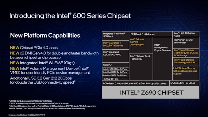
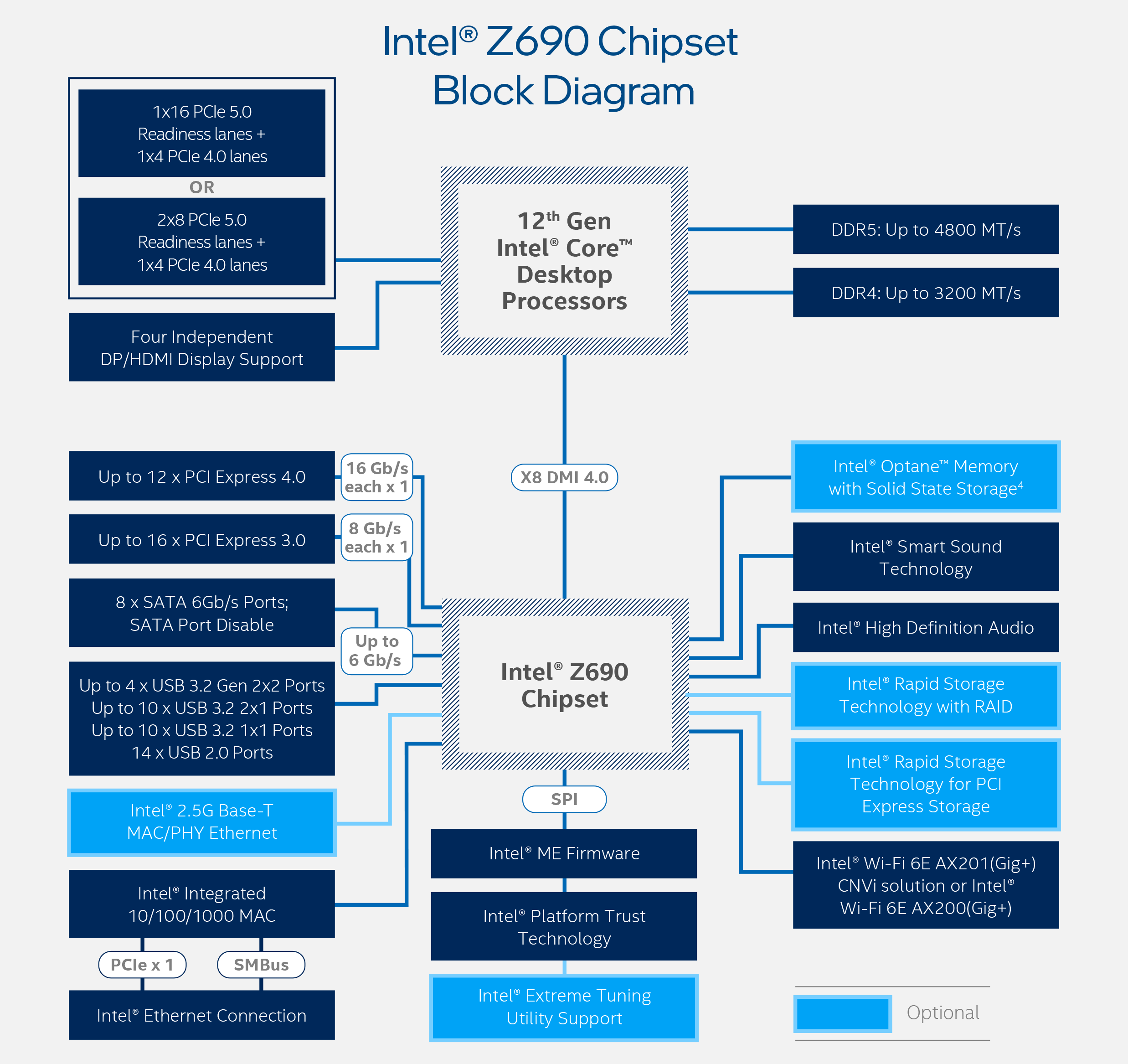
Inside each processor, alongside the 16x PCIe 5.0 lanes for add-in cards and 4x PCIe 4.0 lanes for storage, is an additional link to the chipset. Intel lists this as a DMI 4.0 x8 link, as they use a custom protocol over an effective PCIe physical connection – we asked Intel, and they said the link is rated for 15.76 GB/s, which means the chipset can take two PCIe 4.0 x4 drives at peak before getting near to that limit. This is doubled compared to Z590, which was only 7.88 GB/s.
Today Intel is only announcing its Z690 chipset, built on Intel’s 14nm, and the motherboard manufacturers have about 60+ models to launch in the upcoming week. The processors use a new LGA1700 socket, which means everyone buying the new CPUs also need a new motherboard. Most of the big motherboard companies are holding their own product announcement events, so keep a lookout for those. Each motherboard will support either DDR5 or DDR4, not both, along with enhanced overclocking - more detail on that below.
The Z690 chipset will have 12x PCIe 4.0 lanes and 16x PCIe 3.0 lanes, some of which will be earmarked for general IO use. This includes up to four 20 Gb/s USB ports, up to ten 10 Gb/s USB ports, up to ten 5 Gb/s USB ports, and up to fourteen USB 2.0 ports (although not all at the same time). There are eight SATA ports, along with support for Intel’s onboard RAID. The PCIe storage also now uses Intel’s Volume Management Device (VMD) to assist with PCIe management.
Intel lists an integrated Wi-Fi 6E MAC in the chipset as well, requiring the respective PHY and RF connected over CNVi, which is a proprietary Intel interface – any motherboard manufacturers wanting to use other Wi-Fi 6 solutions will have to directly connect via PCIe as they can’t use the closed standard.
Intel also lists 2.5G Base-T support for wired Ethernet, although that’s a bit of a misnomer here – it’s simply an attached PCIe device using the above-mentioned lanes, and the MAC/PHY still needs to be purchased. This is a similar tactic to previous announcements – users could also add a RAID card in a similar fashion or an FPGA accelerator, however Intel doesn’t highlight those.
Intel’s chipsets employ a great deal of port flexibility – it is essentially a big PCIe switch with a few added extras. It means almost everything that can be attached to a PCIe bus can be used. But with previous generations, there are going to be some limitations with the high-speed IO lanes (such only certain lanes can be used for SATA or Ethernet, limiting perhaps the number of PCIe x4 slots), but some combinations will be better supported than others. Users looking for Thunderbolt 4 support will have to find motherboards with an added controller, as the Alder Lake desktop processors do not have it built-in like the mobile versions.
Intel has not specified the TDP of the Z690 chipset, however we’re yet to see a motherboard with active cooling, so it’s likely to be in that 7-12W range as with previous generations. We expect to see Z690 motherboards range in price from $200 up to $700+, similar to Z590 pricing.
No More TDP: Base Power and Turbo Power
In the past, Intel promoted its processor power as a single number: TDP (Thermal Design Power*). The issue wasn’t so much that this number was wrong, it was because it lacked massive context that wasn’t communicated to anyone. Arguably it took us several years to find out what it really meant, especially in relation to its turbo.
*Technically TDP is defined differently to power consumption, however they are effectively interchangeable at this point, both in common parlance and Intel documentation.
What Intel was promoting wasn’t the power consumption in regular operation, but the guaranteed power consumption for the base processor specifications. That means if a user purchased a six-core processor, base frequency at 3.0 GHz, and a TDP of 65 W, then those are the only specifications that were covered under warranty. Even if the box showcased that the processor was capable of enabling a turbo up to 4.0 GHz, that wasn’t guaranteed. Beyond that, the power consumption of the turbo mode wasn’t specified either, so if the same processor went up to 30-50% higher than 65 W, there was no explicit number from Intel, aside from digging through specification sheets that sometimes weren’t even public, to get a number to help build cooling into the system. It also meant that reviews of hardware that were labeled as 125 W, but consumed 250W+ in turbo mode, weren’t able to accurately demonstrate the scope of the product without additional power monitoring. It got to a point where Intel’s power consumption under turbo became a bit of a meme, and enthusiasts got annoyed that Intel buried this information away.
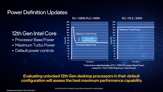
That changes with Alder Lake. Intel is now acknowledging that its turbo mode does indeed have a power increase, and is providing that number alongside the regular set of numbers. To that end, the base ‘TDP’ number of previous generations is gone, and we get two numbers to talk about:
- Processor Base Power (Base): Guaranteed Peak Power at Base Frequency
- Maximum Turbo Power (Turbo): The Maximum Power at full turbo mode that is in spec
So for example, the Processor Base Power (Base) for the Core i9-12900K is set at 125 W. The Maximum Turbo Power is 241 W. This means that systems using this processor will be able to boost up to 241 W if the system is set up to do so, and that is within specification.
For the six processors being announced today, there’s also an added bonus. Under the previous regime, how long a processor could spend in that higher power mode was limited. Intel had a specification for this, which to be honest most motherboard manufacturers ignored anyway, because that length of time was only a guideline, not a rigid specification, and it didn’t break the warranty. Intel is now so confident in its turbo performance, that the new K processors have a default guideline of an unlimited turbo. It should be noted that when Intel launches the rest of the Alder Lake processors, this won’t always be the case.
For users who understand the former PL1/PL2 methodology, it still technically exists under the hood here, where Base is PL1 and Turbo is PL2, but Tau is effectively infinite for K processors.
More in this overview:
- Cache and Hybrid Designs
- Thread Director
- DDR5: Support, XMP, New Features
- Packaging and Overclocking
- Performance and Conclusions
A Hybrid/Heterogeneous Design
Developing a processor with two different types of core is not a new concept – there are billions of smartphones that have exactly that inside them, running Android or iOS, as well as IoT and embedded systems. We’ve also seen it on Windows, cropping up on Qualcomm’s Windows on Snapdragon mobile notebooks, as well as Intel’s previous Lakefield design. Lakefield was the first x86 hybrid design in that context, and Alder Lake is the more mass-market realization of that plan.
A processor with two different types of core disrupts the typical view of how we might assume a computer works. At the basic level, it has been taught that a modern machine is consistent – every CPU has the same performance, processes the same data at the same rate, has the same latency to memory, the same latency to each other, and everything is equal. This is a straightforward homogenous design that’s very easy to write software for.
Once we start considering that not every core has the same latency to memory, moving up to a situation where there are different aspects of a chip that do different things at different speeds and efficiencies, now we move into a heterogeneous design scenario. In this instance, it becomes more complex to understand what resources are available, and how to use them in the best light. Obviously, it makes sense to make it all transparent to the user.
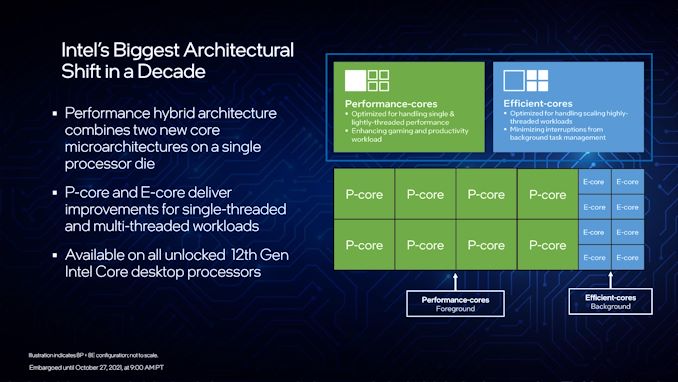
With Intel’s Alder Lake, we have two types of cores: high performance/P-cores, built on the Golden Cove microarchitecture, and high efficiency/E-cores, built on the Gracemont microarchitecture. Each of these cores are designed for different optimization points – P-cores have a super-wide performance window and go for peak performance, while E-cores focus on saving power at half the frequency, or lower, where the P-core might be inefficient.
This means that if there is a background task waiting on data, or something that isn’t latency-sensitive, it can work on the E-cores in the background and save power. When a user needs speed and power, the system can load up the P-cores with work so it can finish the fastest. Alternatively, if a workload is more throughput sensitive than latency-sensitive, it can be split across both P-cores and E-cores for peak throughput.
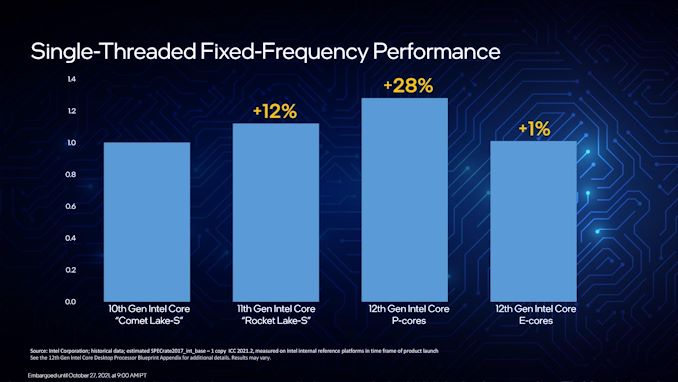
For performance, Intel lists a single P-core as ~19% better than a core in Rocket Lake 11th Gen, while a single E-core can offer better performance than a Comet Lake 10th Gen core. Efficiency is similarly aimed to be competitive, with Intel saying a Core i9-12900K with all 16C/24T running at a fixed 65 W will equal its previous generation Core i9-11900K 8C/16T flagship at 250 W. A lot of that will be that having more cores at a lower frequency is more efficient than a few cores at peak frequency (as we see in GPUs), however an effective 4x performance per watt improvement requires deeper investigation in our review.
As a result, the P-cores and E-cores look very different. A deeper explanation can be found in our Alder Lake microarchitecture deep dive, but the E-cores end up being much smaller, such that four of them are roughly in the same area as a single P-core. This creates an interesting dynamic, as Intel highlighted back at its Architecture Day: A single P-core provides the best latency-sensitive performance, but a group of E-cores would beat a P-core in performance per watt, arguably at the same performance level.
However, one big question in all of this is how these workloads end up on the right cores in the first place? Enter Thread Director (more on the next page).
A Word on L1, L2, and L3 Cache
Users with an astute eye will notice that Intel’s diagrams relating to core counts and cache amounts are representations, and some of the numbers on a deeper inspection need some explanation.
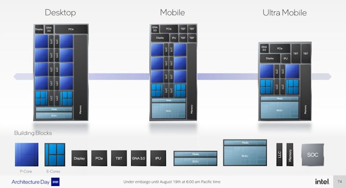
For the cores, the processor design is physically split into 10 segments.
A segment contains either a P-core or a set of four E-cores, due to their relative size and functionality. Each P-core has 1.25 MiB of private L2 cache, which a group of four E-cores has 2 MiB of shared L2 cache.
This is backed by a large shared L3 cache, totaling 30 MiB. Intel’s diagram shows that there are 10 LLC segments which should mean 3.0 MiB each, right? However, moving from Core i9 to Core i7, we only lose one segment (one group of four E-cores), so how come 5.0 MiB is lost from the total L3? Looking at the processor tables makes less sense.
Please note that the following is conjecture; we're awaiting confirmation from Intel that this is indeed the case.
It’s because there are more than 10 LLC slices – there’s actually 12 of them, and they’re each 2.5 MiB. It’s likely that either each group of E-cores has two slices each, or there are extra ring stops for more cache.
Each of the P-cores has a 2.5 MiB slice of L3 cache, with eight cores making 20 MiB of the total. This leaves 10 MiB between two groups of four E-cores, suggesting that either each group has 5.0 MiB of L3 cache split into two 2.5 MiB slices, or there are two extra LLC slices on Intel’s interconnect.
| Alder Lake Cache | |||||||
| AnandTech | Cores P+E/T |
L2 Cache |
L3 Cache |
IGP | Base W |
Turbo W |
Price $1ku |
| i9-12900K | 8+8/24 | 8x1.25 2x2.00 |
30 | 770 | 125 | 241 | $589 |
| i9-12900KF | 8+8/24 | 8x1.25 2x2.00 |
30 | - | 125 | 241 | $564 |
| i7-12700K | 8+4/20 | 8x1.25 1x2.00 |
25 | 770 | 125 | 190 | $409 |
| i7-12700KF | 8+4/20 | 8x1.25 1x2.00 |
25 | - | 125 | 190 | $384 |
| i5-12600K | 6+4/20 | 6x1.25 1x2.00 |
20 | 770 | 125 | 150 | $289 |
| i5-12600KF | 6+4/20 | 6.125 1x200 |
20 | - | 125 | 150 | $264 |
This is important because moving from Core i9 to Core i7, we lose 4xE-cores, but also lose 5.0 MiB of L3 cache, making 25 MiB as listed in the table. Then from Core i7 to Core i5, two P-cores are lost, totaling another 5.0 MiB of L3 cache, going down to 20 MiB. So while Intel’s diagram shows 10 distinct core/LLC segments, there are actually 12. I suspect that if both sets of E-cores are disabled, so we end up with a processor with eight P-cores, 20 MiB of L3 cache will be shown.
Thread Director: Windows 11 Does It Best
Every operating system runs what is called a scheduler – a low-level program that dictates where workloads should be on the processor depending on factors like performance, thermals, and priority. A naïve scheduler that only has to deal with a single core or a homogenous design has it pretty easy, managing only power and thermals. Since those single core days though, schedulers have grown more complex.
One of the first issues that schedulers faced in monolithic silicon designs was multi-threading, whereby a core could run more than one thread simultaneously. We usually consider that running two threads on a core usually improves performance, but it is not a linear relationship. One thread on a core might be running at 100%, but two threads on a single core, while overall throughput might increase to 140%, it might mean that each thread is only running at 70%. As a result, schedulers had to distinguish between threads and hyperthreads, prioritizing new software to execute on a new core before filling up the hyperthreads. If there is software that doesn’t need all the performance and is happy to be background-related, then if the scheduler knows enough about the workload, it might put it on a hyperthread. This is, at a simple level, what Windows 10 does today.
This way of doing things maximizes performance, but could have a negative effect on efficiency, as ‘waking up’ a core to run a workload on it may incur extra static power costs. Going beyond that, this simple view assumes each core and thread has the same performance and efficiency profile. When we move to a hybrid system, that is no longer the case.
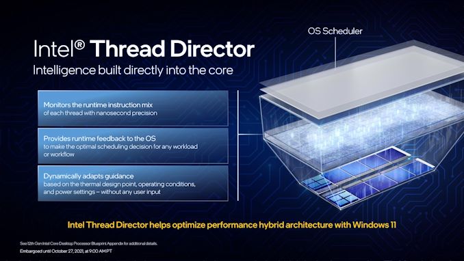
Alder Lake has two sets of cores (P-cores and E-cores), but it actually has three levels of performance and efficiency: P-cores, E-Cores, and hyperthreads on P-cores. In order to ensure that the cores are used to their maximum, Intel had to work with Microsoft to implement a new hybrid-aware scheduler, and this one interacts with an on-board microcontroller on the CPU for more information about what is actually going on.
The microcontroller on the CPU is what we call Intel Thread Director. It has a full scope view of the whole processor – what is running where, what instructions are running, and what appears to be the most important. It monitors the instructions at the nanosecond level, and communicates with the OS on the microsecond level. It takes into account thermals, power settings, and identifies which threads can be promoted to higher performance modes, or those that can be bumped if something higher priority comes along. It can also adjust recommendations based on frequency, power, thermals, and additional sensory data not immediately available to the scheduler at that resolution. All of that gets fed to the operating system.
The scheduler is Microsoft’s part of the arrangement, and as it lives in software, it’s the one that ultimately makes the decisions. The scheduler takes all of the information from Thread Director, constantly, as a guide. So if a user comes in with a more important workload, Thread Director tells the scheduler which cores are free, or which threads to demote. The scheduler can override the Thread Director, especially if the user has a specific request, such as making background tasks a higher priority.
What makes Windows 11 better than Windows 10 in this regard is that Windows 10 focuses more on the power of certain cores, whereas Windows 11 expands that to efficiency as well. While Windows 10 considers the E-cores as lower performance than P-cores, it doesn’t know how well each core does at a given frequency with a workload, whereas Windows 11 does. Combine that with an instruction prioritization model, and Intel states that under Windows 11, users should expect a lot better consistency in performance when it comes to hybrid CPU designs.
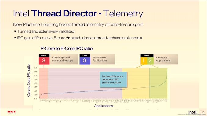
Under the hood, Thread Director is running a pre-trained algorithm based on millions of hours of data gathered during the development of the feature. It identifies the effective IPC of a given workflow, and applies that to the performance/efficiency metrics of each core variation. If there’s an obvious potential for better IPC or better efficiency, then it suggests the thread is moved. Workloads are broadly split into four classes:
- Class 3: Bottleneck is not in the compute, e.g. IO or busy loops that don’t scale
- Class 0: Most Applications
- Class 1: Workloads using AVX/AVX2 instructions
- Class 2: Workloads using AVX-VNNI instructions
Anything in Class 3 is recommended for E-cores. Anything in Class 1 or 2 is recommended for P cores, with Class 2 having higher priority. Everything else fits in Class 0, with frequency adjustments to optimize for IPC and efficiency if placed on the P-cores. The OS may force any class of workload onto any core, depending on the user.
There was some confusion in the press briefing as to whether Thread Director can ‘learn’ during operation, and how long it would take – to be clear, Thread Director doesn’t learn, it already knows from the pre-trained algorithm. It analyzes the instruction flow coming into a core, identifies the class as listed above, calculates where it is best placed (which takes microseconds), and communicates that to the OS. I think the confusion came with the difference in the words ‘learning’ and ‘analyzing’. In this case, it’s ‘learning’ what the instruction mix to apply to the algorithm, but the algorithm itself isn’t updated in the way that it is ‘learning’ and adjusting the classes. Ultimately even if you wanted to make the algorithm self-learn your workflow, the algorithm can’t actually see which thread relates to which program or utility – that’s something on the operating system level, and down to Microsoft. Ultimately, Thread Director could suggest a series of things, and the operating system can choose to ignore them all. That’s unlikely to happen in normal operation though.
One of the situations where this might rear its head is to do with in-focus operation. As showcased by Intel, the default behavior of Windows changes depending on whether on the power plan.
When a user is on the balanced power plan, Microsoft will move any software or window that is in focus (i.e. selected) onto the P-cores. Conversely, if you click away from one window to another, the thread for that first window will move to an E-core, and the new window now gets P-core priority. This makes perfect sense for the user that has a million windows and tabs open, and doesn’t want them taking immediate performance away.
However, this way of doing things might be a bit of a concern, or at least it is for me. The demonstration that Intel performed was where a user was exporting video content in one application, and then moved to another to do image processing. When the user moved to the image processing application, the video editing threads were moved to the E-cores, allowing the image editor to use the P-cores as needed.
Now usually when I’m dealing with video exports, it’s the video throughput that is my limiting factor. I need the video to complete, regardless of what I’m doing in the interim. By defocusing the video export window, it now moves to the slower E-cores. If I want to keep it on the P-cores in this mode, I have to keep the window in focus and not do anything else. The way that this is described also means that if you use any software that’s fronted by a GUI, but spawns a background process to do the actual work, unless the background process gets focus (which it can never do in normal operation), then it will stay on the E-cores.
In my mind, this is a bad oversight. I was told that this is explicitly Microsoft’s choice on how to do things.
The solution, in my mind, is for some sort of software to exist where a user can highlight programs to the OS that they want to keep on the high-performance track. Intel technically made something similar when it first introduced Turbo Max 3.0, however it was unclear if this was something that had to come from Intel or from Microsoft to work properly. I assume the latter, given the OS has ultimate control here.
I was however told that if the user changes the Windows Power Plan to high-performance, this behavior stops. In my mind this isn’t a proper fix, but it means that we might see some users/reviews of the hardware with lower performance if the workload doing the work is background, and the reviewer is using the default Balanced Power Plan as installed. If the same policy is going to apply to Laptops, that’s a bigger issue.
Memory: Varies with Number of Modules
Inside each of the Alder Lake processors are memory controllers for both DDR5 and DDR4. Unlike previous generations, we’re unlikely to see motherboards supporting both types of memory. We understand that Intel has explicitly requested this – we didn’t see many retail combo boards in the DDR3/DDR4 era, so expect to see fewer this time around (although you can imagine someone will eventually do it). There is a slight technical reason too – DDR5 uses onboard power management, while DDR4 requires that from the motherboard, something which is hard to implement without wholly independent traces for both. If Intel is saying both cannot be done at the same time, then it’s likely that this is a unified DDR4+DDR5 controller that shares an amount of logic internally, but only one can be used at any one time.
Intel lists the specifications for its memory support as DDR4-3200 and DDR5-4800, and as always memory support is listed as conforming to the JEDEC implementations. This means Intel qualifies DDR4-3200 CL22, and anything above that is technically overclocking the CPU – it’s actually hard to find consumer memory at this speed these days. For DDR5, there are actually three specifications here:
| DDR5 JEDEC Specifications | |||||||
| AnandTech | Data Rate MT/s |
CL |
Peak BW GB/s |
Latency (ns) |
|||
| DDR5-4800 | A | 4800 | 34 | 34 | 34 | 38.40 | 14.17 |
| B | 40 | 40 | 40 | 16.67 | |||
| C | 42 | 42 | 42 | 17.50 | |||
We clarified with Intel that the processor supports all three, with the top being DDR5-4800A CL34. This is despite Intel shipping DDR5-4800B CL40 with their press kits, but I digress.
The thing with memory support is that it usually quoted for a specific number of modules installed into the system. In this case, Intel is quoting these numbers using one module per channel (technically a 64-bit channel, but more on that later), meaning that these are the supported speeds when two memory modules are supported. The official supported speed changes if you have more memory, double-sided memory, or dual rank memory.
We’ve seen this before – server processors are notorious for having slower support when more memory modules are installed. It turns out the more bandwidth you need, the harder it is to keep that speed with higher capacity memory. It was only until Intel’s 11th Gen Core products that the memory design supported DDR4-3200 regardless of configuration, because sometimes that’s how long it takes to optimize a memory controller. For Alder Lake, DDR4-3200 is also supported in any configuration, but DDR5 changes depending on the memory.
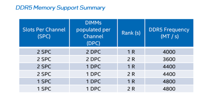
Intel shared this table with us.
If the motherboard has two memory slots total, then the maximum support is DDR5-4800 in any configuration.
If the motherboard has four memory slots total, then the maximum support is DDR5-4400 when two slots are filled with any memory.
If all four memory slots are filled, single rank memory will support up to DDR5-4000.
If all four memory slots are filled, dual-rank memory will support up to DDR5-3600.
So technically Intel listing memory support on Alder Lake as DDR5-4800 is a bit of a misdirection compared to previous launches. If we were to look at parity, two modules in a four-slot board, then really we’d be quoting DDR5-4400. Funnily enough, all of Intel’s benchmarks presented at this launch were run at DDR5-4400, as per specification. Kudos to the testing team to staying within those guidelines.
A side note here on memory channels as a whole. In the desktop space, we’re used to one memory module having memory for one 64-bit memory channel. That’s true for DDR4, DDR3, DDR2 etc, but the DDR5 specifications move to 32-bit memory channels. So while each DDR5 module is still using 64-bits of bandwidth, there are technically two 32-bit memory channels worth of memory on each module. This can create a little bit of confusion, because it means that Intel 12th Gen, while still a 128-bit memory interface as previous generations, it uses 4x 32-bit channels, not 2x 64-bit. Undoubtedly companies (even Intel) still call this dual-channel, as a channel is usually inferred to be a 64-bit interface.
There is no easy solution here. 2DPC (two modules per channel) doesn’t really mean much if technically channel there infers 64-bit but you’re running on a 2x32-bit channel system. Some users are calling a DDR5 module a ’channel’ with two 32-bit ‘sub-channels’, although that is more a twisting of reality, given that sub-channels are often something else in memory design. Because we’ve used the word ‘module’ to imply a 64-bit channel for so long, and because memory can be installed with more than one module per 64-bit channel, it’s actually a mess in English to find not only the correct words but also ones simple enough to not make the situation overly complex. Perhaps it’s time for some new words.
Memory: XMP 3.0 and Better SPD
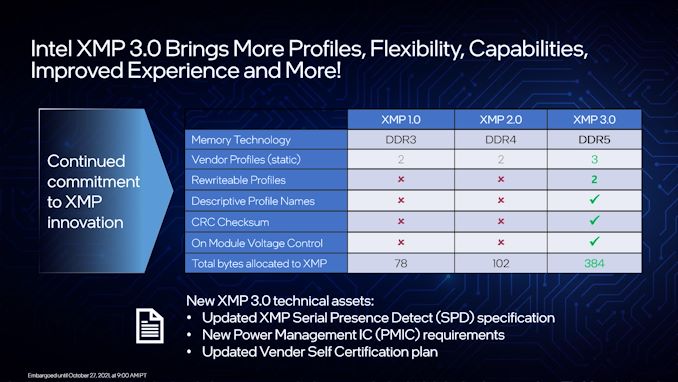
One of the new features with DDR5 is the expansion of Intel’s eXtreme Memory Profile support. Now moving to XMP 3.0, it increases flexibility for both users and vendors by increasing the number of profiles per module, opening up for customization, and improving the overclocking experience.
Memory vendors when they ship the memory will embed in the memory firmware a series of specifications, known as SPDs. For standard memory running to JEDEC specifications, the module will likely contain SPD profiles relating to something slow for underlying support, and then up to what the memory chips were sold at – depending on the motherboard, the system then picks the JEDEC SPD profile that best fits the processor (I’ve seen a wild variety of implementation here, funnily enough.
XMP goes above and beyond traditional SPD support.
XMP 2.0 on DDR4 contains up to two additional SPD profiles with overclocked values. For example, a DDR4-4000 CL16 memory module might have three profiles total – one at 2133 CL15, one at 3200 CL22, and a third XMP profile at 4000 CL16. It is up to the user to then select that profile when in the BIOS or through additional software. If the module has two XMP profiles, perhaps one for latency and another for bandwidth, then this can be done in XMP 2.0.
The update to XMP 3.0 allows for five profiles, rather than two. Three of these profiles are memory module vendor locked, limited by whatever they come out of the factory at. The final two profiles can be used by the memory module vendor, but are re-writable by users in order to save overclocking settings. These profiles can also be named to be descriptive.
Intel states that this re-writing process is backed by a rigorous checksum support so users can’t brick their hardware. For most situations, that’s going to be reasonable, however if that security does get broken, it might be advised that if you buy second-hand DDR5 to erase those profiles and not use them. Just in case it overvolts the memory controller to 3 volts, or something.
Alongside more profiles, because DDR5 moves the power management for the module onto the module itself, if a memory vendor uses a ‘better than base’ solution then users can adjust various voltages and timings on a per-module basis.
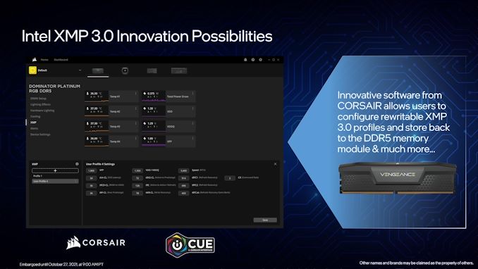
Both the profile expansion and the updated voltage controls are also now exposed to the operating system in such a way that allows for better software implementation. Users with Corsair memory, for example, can use Corsair software to adjust the memory on the fly and monitor temperatures, power, voltages, and also keep track of how they fluctuate during overclocking, testing, or normal use. There is also another new feature, allowing users to adjust memory frequency on the fly, which has never been seen before. We’ll cover that in the next section.
On a more ecosystem level, we confirmed with Intel that XMP 3.0 is a self-certification procedure at memory vendors, with no additional licensing costs to the vendors.
Memory Gets Turbo: Dynamic Memory Boost
One of the persistent features with memory over the years is that when you have settings saved in the BIOS, they are ‘trained’ (tested to work) when the system boots up, and then that’s what you have for the whole time that the system is turned on. It never slows down, it never duty cycles to reduce power – it has been very consistent for a long time.
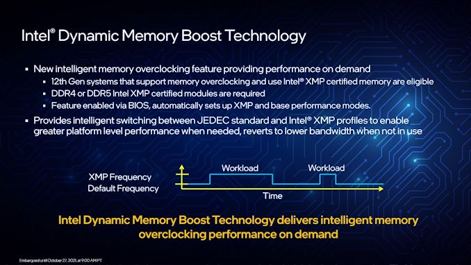
With Intel’s Z690 boards and 12th Gen Core Alder Lake processors, that changes. Much like processors and graphics have had idle states and turbo states for generations, memory now gets it as well.
This first-generation technology is basic, but a start. A 12th Gen system, as long as it runs DDR4 or DDR5 memory with XMP, can define two of the onboard SPD profiles – one as the base, and one as the turbo. Usually the base profile is one of the immutable JEDEC profiles, and the turbo is an XMP profile. But when activated, the system is able to switch on the fly between the two, activating when a workload is initiated for higher performance, and supposedly better idle efficiency.
There are a few thoughts or questions on this worth noting:
#1: It works on DDR4? Intel says yes. This makes it sound like this is more of a software/firmware innovation than a hardware innovation, or it requires the right hardware on the CPU at least. No doubt if it works, it will become ubiquitous.
#2: Isn’t power efficiency really for benchmarks and laptops? I agree with this one, and expect it to be more of a highlighted feature when Alder Lake comes to laptops and notebooks. That being said, most notebook DRAM is JEDEC anyway, so it might open the doors for better-overclocked notebook memory if it can retain the battery life of a base JEDEC profile. Either that, or notebook memory will use a fast JEDEC profile in operation, then move to a more efficient but slower JEDEC profile on idle to save power.
#3: Doesn’t this introduce instability? Perhaps, but if it’s handled in the same way CPU turbo can be, then it shouldn’t be an issue.
In the same way we look to measure how CPU frequency ramps up from a performance request, we will have to look into tools to measure the same thing on memory, especially if more than a simple base/turbo system is developed for future use.
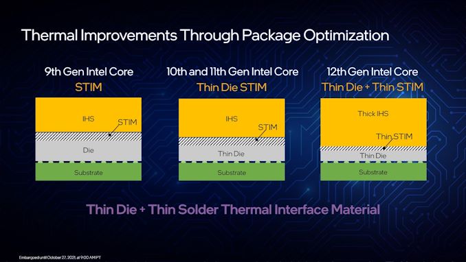
Package Improvements
As we move to smaller process nodes, the thermal density of high-performance silicon becomes more of an issue, and so all the processor companies put resources into their mechanical design teams to come up with a solution for the best thermal performance but also comes in line with costs. For example, we’ve seen Intel over the years transition from a soldered down heatspreader, to liquid metal, to basic thermal paste (because saving 0.1 cents means a lot across 70m CPUs), and then all the way back again when customers started demanding it.
However, in that time, we’ve pretty much kept the same socket design for mainstream processors. There hasn’t been much emphasis on changing the design itself for thermomechanical improvements in order to retain reuse and compatibility. There have been some minor changes here and there, such as substrate thinning, but nothing that substantial. The move to a new socket for Alder Lake now gives Intel that opportunity.
For Alder Lake, Intel is using an optimized packaging process to reduce the amount of soldered thermal material used in the processors. Combining that with a thinner die, and Intel is having to increase the thickness of the heatspreader to maintain the required z-height for the platform. The idea here is that the limiting factor in the cooling solution is any time we have a thermal interface, from one material to another – in this case, die to solder, and solder to heatspreader. Solder is the weak point here, so if the heatspreader gets thicker to meet the die, then less solder is needed.
Ultimately direct-die liquid cooling would be the boon here, but Intel has to come up with a solution that fits millions of processors. We have seen Intel offer different packaging solutions based on the SKU itself, so it will be interesting if the mid-range still get the Thin Die + Thin STIM treatment, or if they’ll go back to the cheap thermal paste.
Overclocking: We Have Headroom
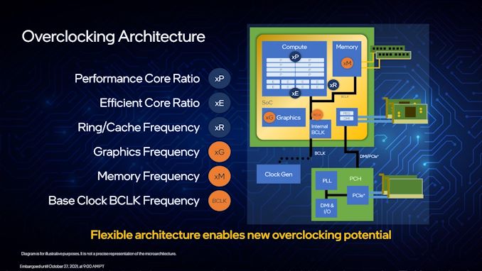
It wouldn’t be too much of a leap to say that for most users, the only useful overclocking they might want to look at is enabling XMP on their memory. Modern processors these days are so close to their actual voltage and thermal limits out of the box these days that even if there was 200-300 MHz to gain, especially for the top Core i9 parts, it wouldn’t be worth the +100W it produces. I’m also getting to an age now where I prefer a good stable system, rather than eking out every frame, but having lived in the competitive OC scene for a while, I understand the drive that a lot of those users have to go above and beyond. To that end, Intel is introducing a few new features, and reviving some old ones, for Alder Lake.
Alder Lake also complicates things a bit with the P-core and E-core design.
To start, all the cores on the K/KF parts can be overclocked. The P-cores can be overclocked individually, whereas the E-cores are in groups of four. All the E-cores can be disabled, but at least one P-core needs to be enabled for the system to work (this has interesting consequences for Intel’s design). All cores can have additional AVX offsets, per-core ratio and voltage controls, and the ring/uncore ratios can also be adjusted. Memory also has the bells and whistles mentioned on a previous page. Those with integrated graphics can also be adjusted.
What Alder Lake brings back to the table is BCLK overclocking. For the last decade or so, most overclocking is done with the CPU multiplier, and before that it was BCLK or FSB. Intel is now saying that BCLK overclocking has returned, and this is partly due to motherboard customizations in the clock generator. Every Alder Lake CPU has an internal BCLK/clock generator it can use, however motherboard vendors can also apply an external clock generator. Intel expects only the lowest-end motherboards will not have an external generator.
The use of two generators allows the user to overclock the PCIe bus using the external generator, while maintaining a regular BCLK on other parts of the system with the internal clock. The system can also apply voltage in an adaptive way based on the overclock, with additional PLL overrides.
On top of this, Intel is integrating more user-accessible telemetry for its cores, particularly the E-cores, and real-time frequency analysis. On top of this, users can adjust the memory frequency in the operating system, rather than having to reboot – this is an extension of the memory turbo functionality previously mentioned.
For regular users, Intel is also offering a one-click immediate overclock feature. On launch, the Core i9 will be supported and overclock the P-cores +100 MHz and the E-cores +300 MHz immediately. It sounds like Intel is confident that all CPUs will be able to do this, but they want it to be user selectable. Beyond that, I confirmed the tool does still void the warranty. Intel’s VP dismissed it as an issue, citing that the recent overclocker warranty program they canned had such a low pickup, it wasn’t worth continuing. I’d say that the two things are mutually exclusive, but that’s up to Intel.
Performance
I’m not a big one on posting first-party benchmark results, but the high-level overview from Intel was this:
- At 3.3 GHz, 12900K is +19% better in Single Thread Performance over the 11900K
- Over the 11900K, the 12900K is +19% better at 1080p High with RTX 3090
- Over the 11900K, the 12900K gets +84% better fps when concurrently streaming
- Over the 11900K, the 12900K is +22-100% better in content creation (Adobe)
- Over the 11900K, the 12900K is +50% faster in BlenderMT at 241W (vs 250W)
- Over the 11900K, the 12900K performs the same in BlenderMT at only 65W (vs 250W)
All of Intel’s tests were using Windows 11, with DDR5-4400 vs DDR4-3200. Intel did have a small one slide of comparisons against AMD in gaming with an RTX 3090, however they stated they were done without the latest L3 patch fix, and admitted that they would have preferred to show us full results. By the time this article goes live, we may have seen those results at Intel’s event.
This is a reasonable set of data, very focused on the Core i9, but when the reviews come out we’ll be able to see where it sits compared to the other parts, as well as the competition. The only thing that concerns me right now leading up to the launch is the behavior of demoting workloads to E-cores when not in focus when on the Balanced Power Plan (mentioned on the Thread Director page). It won’t be until I get hands-on with the hardware as to whether I see it as an issue or not.
Another factor to mention is DRM. Intel has made statements to this, but there is an issue with Denuvo as it uses part of the CPU configuration to identify systems to stop piracy. Due to the hybrid nature, Denuvo might register starting on a different core (P vs E) as a new system, and eventually lock you out of the game either temporarily or permanently. Out of the top 200 games, around 20 are affected and Intel says it still has a couple more to fix. It’s working with Denuvo for a high-level fix from their side, and with developers to fix from their end as well. Intel says it’s a bit harder with older titles, especially when there’s no development going on, or the IP is far away from its original source. A solution to this would be to only launch those games on specific cores, but look out for more updates as time marches on.
Conclusions
Well, it’s almost here. It looks like Intel will take the ST crown, although MT is a bit of a different story, and might rely explicitly on the software being used or if the difference in performance is worth the price. The use of the hybrid architecture might be an early pain point, and it will be interesting to see if Thread Director remains resilient to the issues. The bump up to Windows 11 is also another potential rock in the stream, and we’re seeing some teething issues from users, although right now users who are looking to early adopt a new CPU are likely more than ready to adopt a new version of Windows at the same time.
The discourse on DDR4 vs DDR5 is one I’ve had for almost a year now. Memory vendors seem ready to start seeding kits to retailers, however the expense over DDR4 is somewhat eyewatering. The general expectation is that DDR5 won’t offer much performance uplift over a good kit of DDR4, or might even be worse. The benefit of DDR5 then at this point is more to start on that DDR5 ladder, where the only way to go is up. This will be Intel’s last DDR4 platform on desktop it seems.
On the processors themselves, the Core i5 and Core i7 parts look very competitive and in line with respective popular AMD processors. Both the Core i5 and Core i7 have extra E-cores, so we’ll see if that comes in handy for extra performance, or they’ll just end up burning power and performance per watt needs re-examining. The Core i9 challenge is probably sided on Intel for single thread, but all the questions will be over proper multi-threaded performance.
| Intel 12th Gen Core, Alder Lake | |||||||||
| AnandTech | Cores P+E/T |
E-Core Base |
E-Core Turbo |
P-Core Base |
P-Core Turbo |
IGP | Base W |
Turbo W |
Price $1ku |
| i9-12900K | 8+8/24 | 2400 | 3900 | 3200 | 5200 | 770 | 125 | 241 | $589 |
| i9-12900KF | 8+8/24 | 2400 | 3900 | 3200 | 5200 | - | 125 | 241 | $564 |
| i7-12700K | 8+4/20 | 2700 | 3800 | 3600 | 5000 | 770 | 125 | 190 | $409 |
| i7-12700KF | 8+4/20 | 2700 | 3800 | 3600 | 5000 | - | 125 | 190 | $384 |
| i5-12600K | 6+4/20 | 2800 | 3600 | 3700 | 4900 | 770 | 125 | 150 | $289 |
| i5-12600KF | 6+4/20 | 2800 | 3600 | 3700 | 4900 | - | 125 | 150 | $264 |
After not much CPU news for a while, it’s time to get in gear and find out what Intel has been cooking. Come back on November 4th for our review.

