Original Link: https://www.anandtech.com/show/16818/intel-accelerated-webcast-on-july-26th-update-on-process-technology-and-roadmaps
Intel Accelerated Webcast on July 26th: Update on Process Technology and Roadmaps
by Dr. Ian Cutress on July 12, 2021 10:51 AM EST- Posted in
- CPUs
- Intel
- GPUs
- 10nm
- 7nm
- Packaging
- 3D Packaging
- IFS
- Intel Foundry Services
_678x452.jpg)
Earlier this year, new Intel CEO Pat Gelsinger outlined his new ‘IDM 2.0’ vision for Intel. This vision was a three-pronged strategy based on improving its own process node technology, mixing in other foundry technology where needed, and also realigning its manufacturing for a new foundry service offering allowing other semiconductor companies to use Intel’s manufacturing expertise. As part of the journey towards Gelsinger’s IDM 2.0 vision, we were told to expect updates at a more regular cadence, and the announcement of ‘Intel Accelerated’ in a couple of weeks is the next event on the calendar.
Intel IDM 2.0
As AnandTech reported back in March, Intel’s IDM 2.0 strategy features the following:
- Build (on Intel 7nm)
- Expand (use TSMC and others)
- Productize (Intel Foundry Services)
Previously Intel was almost completely insular, preferring to use its own technologies almost exclusively, and it kept them to itself. Through IDM 2.0, CEO Pat Gelsinger is hoping to drive Intel’s next wave of products by using the best the market has to offer, but also expand Intel’s own manufacturing to new customers as a potential revenue stream. The guise of this development is also in the sense of aligning semiconductor manufacturing outside of Asia, to make other areas of the world less reliant on a single resource.
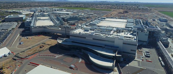
Part of this strategy requires Intel to execute on its research roadmaps. Intel’s struggles to enable 10nm in suitably high volumes have been the focus of plenty of column inches, and while Intel is now shipping 10nm Tiger Lake-H in the millions* and 10nm Ice Lake Xeons in the hundreds of thousands*, there is a need to address the future of Intel’s manufacturing. This means making sure it aligns with commercial interests and enables a competitive offering against the competition. This covers not only manufacturing, to which Intel announced a $20b investment in its Arizona manufacturing earlier this year, but also advanced packaging technologies, where Intel announced a $3.5b investment in its New Mexico facilities in May.

Intel's Ocotillo Campus, Arizona
Part of creating its Intel Foundry Services offering for external parties to use Intel manufacturing relies on Intel being more open about its technology and showcasing progress in its research and development, perhaps to a degree more than it has done in the past. Any future customers of Intel’s IP portfolio will want to know what is coming down the pipe, especially when silicon development takes years and getting the right timing in the alignment of technologies becomes very important in these competitive markets. Having a platform to showcase Intel’s roadmaps is what this upcoming Intel Accelerated Webcast seems to be about.
Intel Accelerated
On Monday July 26th, 2pm Pacific, Intel will livestream its Intel Accelerated webcast. The topics of the day are presentations from CEO Pat Gelsinger and Dr. Ann Kelleher on Intel’s process node technology development and roadmaps into Intel’s packaging portfolio. Dr. Ann Kelleher is Intel’s SVP and GM of Technology Development, and the person in charge of all of this.
We are hoping that this webcast will go into detail as to where Intel expects its 10nm development to go on SuperFin/Enhanced SuperFin, leading into discussions about 7nm. While Intel won’t be discussing things like buried power rails or new manufacturing techniques, we will hopefully see a disclosure more akin to TSMC and Samsung’s Foundry events that happen yearly regarding what variations of process node development are being targeted.
On the packaging front, we know that Intel has EMIB, Foveros, and ODI under research up against TSMC’s 3DFabric, so insights into how Intel is developing its technology will be welcome by both the semiconductor industry but also the financial markets. Interestingly enough, while this event is on the 26th, Intel’s quarterly financial disclosures are on the 22nd, a few days prior. On Intel’s packaging, as the company moves into its Client 2.0 strategy of drilling everything down into silicon IP blocks, understanding exactly how those will all be connected becomes a vital element to the future of Intel.
The event will be open to all on Intel’s Newsroom.


