Original Link: https://www.anandtech.com/show/16594/intel-3rd-gen-xeon-scalable-review
Intel 3rd Gen Xeon Scalable (Ice Lake SP) Review: Generationally Big, Competitively Small
by Andrei Frumusanu on April 6, 2021 11:00 AM EST- Posted in
- CPUs
- Intel
- Xeon
- Enterprise
- Servers
- Xeon Scalable
- Ice Lake-SP
Section by Ian Cutress
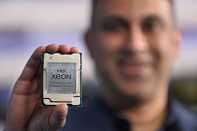
The launch of Intel’s Ice Lake Xeon Scalable processors has been in the wings for a number of years. The delays to Intel’s 10nm manufacturing process have given a number of setbacks to all of Intel’s proposed 10nm product lines, especially the high performance Xeon family: trying to craft 660 mm2 of silicon on a process is difficult at the best of times. But Intel has 10nm in a place where it is economically viable to start retailing large Xeon processors, and the official launch today of Intel’s 3rd Generation Xeon Scalable is on the back of over 200,000+ units shipped to major customers to date. The new flagship, the Xeon Platinum 8380, has 40 cores, offers PCIe 4.0, and takes advantage of the IPC gain in Intel’s Sunny Cove processor core. We’re testing it against the best in the market.
Intel’s 3rd Generation Xeon Scalable: 10nm Goes Enterprise
Today Intel is launching the full stack of processors under the 3rd Generation Xeon Scalable Ice Lake branding, built upon its 10nm process. These processors, up to 40 cores per socket, are designed solely for single socket and dual socket systems, competing in a market with other x86 and Arm options available. With this new generation, Intel’s offering is aimed to be two-fold: first, the generational uplift compared to 2nd Gen, but also the narrative around selling a solution rather than simply selling a processor.
Intel’s messaging with its new Ice Lake Xeon Scalable (ICX or ICL-SP) steers away from simple single core or multicore performance, and instead is that the unique feature set, such as AVX-512, DLBoost, cryptography acceleration, and security, along with appropriate software optimizations or paired with specialist Intel family products, such as Optane DC Persistent Memory, Agilex FPGAs/SmartNICs, or 800-series Ethernet, offer better performance and better metrics for those actually buying the systems. This angle, Intel believes, puts it in a better position than its competitors that only offer a limited subset of these features, or lack the infrastructure to unite these products under a single easy-to-use brand.
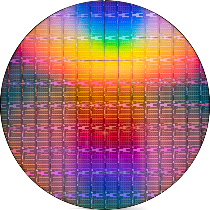
An Wafer of 40-core Ice Lake Xeon 10nm Processors
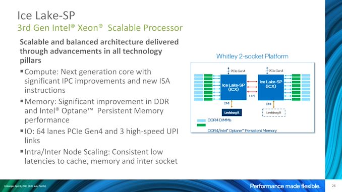
Nonetheless, the launch of a new generation of products and an expanded portfolio warrants the product to actually be put under test for its raw base performance claims. This generation of Xeon Scalable, Intel’s first on 10nm, uses a newer architecture Sunny Cove core. Benefits of this core, as explained by Intel, start with an extra 20% raw performance increase, enabled through a much wider core with an improved front end and a more execution resources. Outside of the core, memory bandwidth is improved both by increasing memory channels from six to eight, but also new memory prefetch techniques and optimizations that increases bandwidth up to 100% with another +25% efficiency. The mesh interconnect between the cores also uses updated algorithms to feed IO to and from the cores, and Intel is promoting better power management through independent power management agents inside each IP block.
On top of this, Intel is layering on accelerative features, stating that over the raw performance, software optimized for these accelerators will see a better-than-generational uplift. This starts with the basic core layout, especially as it pertains to SIMD commands such as SSSE, AVX, AVX2, and AVX-512: Intel is enabling better cryptography support across its ISA, enabling AES, SHA, GFNI, and other instructions to run simultaneously across all vector instruction sets. AVX-512 has improved frequencies during more complex bit operations for ICX with smarter mapping between instructions and power draw, offering an extra 10% frequency for all 256-bit instructions. On top of this is Intel’s Speed Select Technologies, such as Performance Profile, Base Frequency improvements, Turbo Frequency improvements, and Core Power assistance to ensure peak per-core performance or quality of service during a heavily utilized system depending on customer requirements. Other new features include Software Guard Extensions, enabling enclave sizes up to 512 GB per socket with select models.
Ice Lake’s Sunny Cove Core: Part 2
The Sunny Cove core has actually already been in the market. Intel has made a consumer variant of the core and a server variant of the core. Ice Lake Xeon has the server variant, with bigger caches and slightly different optimization points, but it’s the consumer variant that we have seen and tested in laptop form. Sunny Cove is part of Intel’s Ice Lake notebook processor portfolio, which we reviewed the performance back on August 1st 2019, which 614 days ago. That length of time between enabling a core for notebooks and enabling the same core (with upgrades for servers) on enterprise is almost unheard of, but indicative of Intel’s troubles in manufacturing.
Nonetheless, in our notebook testing of the Ice Lake core, we saw a raw +17-18% performance over the previous generation, however this was at the expense of 15-20% in frequency. Where the product truly excelled was in memory limited scenarios, where a new memory controller provided better-than-generational uplift. When it comes to this generation of Xeon Scalable processors with the new core, as you see in the review, in non-accelerated workloads we get very much a similar story. That being said, consumer hardware is very often TDP limited, especially laptops! With the new Ice Lake Xeon platform, Intel is boosting the peak TDP from 205 W to 270 W, which also gives additional performance advantages.
The Headline Act: Intel’s Xeon Platinum 8380
The head prefect of Intel’s new processor lineup is the Platinum 8380 - a full fat 40 core behemoth. If we put it side by side with the previous generation processors, there some key specifications to note.
| Intel Xeon Comparison: 3rd Gen vs 2nd Gen Peak vs Peak |
||
| Xeon Platinum 8380 |
AnandTech | Xeon Platinum 8280 |
| 40 / 80 | Cores / Threads | 28 / 56 |
| 2900 / 3400 / 3000 | Base / ST / MT Freq | 2700 / 4000 / 3300 |
| 50 MB + 60 MB | L2 + L3 Cache | 28 MB + 38.5 MB |
| 270 W | TDP | 205 W |
| PCIe 4.0 x64 | PCIe | PCIe 3.0 x48 |
| 8 x DDR4-3200 | DRAM Support | 6 x DDR4-2933 |
| 4 TB | DRAM Capacity | 1 TB |
| 200-series | Optane | 100-series |
| 4 TB Optane + 2 TB DRAM |
Optane Capacity Per Socket |
1 TB DDR4-2666 + 1.5 TB |
| 512 GB | SGX Enclave | None |
| 1P, 2P | Socket Support | 1P, 2P, 4P, 8P |
| 3 x 11.2 GT/s | UPI Links | 3 x 10.4 GT/s |
| $8099 | Price (1ku) | $10099* 6258R, 2P Variant is only $3950 |
Between these processors, the new flagship has a number of positives:
- +43% more cores (40 vs 28),
- nearly double the cache,
- +33% more PCIe lanes (64 vs 48),
- 2x the PCIe bandwidth (PCIe 4.0 vs PCIe 3.0)
- 4x the memory support (4 TB vs 1 TB)
- SGX Enclave support
- +7% higher socket-to-socket bandwidth
- Support for DDR4-3200 Optane DCPMM 200-series
- Price is down 20%... or up 100% if you compare to 6258R
Though we should perhaps highlight some of the negatives:
- TDP is up +32% (270 W vs 205 W)
- ST Frequency is down (3400 MHz vs 4000 MHz)
- MT Frequency is down (3000 MHz vs 3300 MHz)
If we combine the specification sheet cores and all-core (MT) frequency, Ice Lake actually has about the same efficiency here as the previous generation. Modern high-performance processors often operate well outside the peak efficiency window, however Ice Lake being at a lower frequency would usually suggest that Ice Lake is having to operate closer to the peak efficiency point to stay within a suitable socket TDP than previous generations. This is similar to what we saw in the laptop space.
Features across all Ice Lake Xeon Scalable processors
We’ll dive into the different processors over on the next page, however it is worth noting some of the key features that will apply to all of Intel’s new ICL-SP family. Across the ~40 new processors, including all the media focused parts, the network focused processors, and all the individual optimizations used, all of the processors will have the following:
All Ice Lake Xeons will support eight channels of DDR4-3200 at 2DPC(new info)- All Ice Lake Xeons will support 4 TB of DRAM per socket
- All Ice Lake Xeons will support SGX Enclaves (size will vary)
- All Ice Lake Xeons will support 64x PCIe 4.0 lanes
- All Ice Lake Xeons will support 2x FMA
- Platinum/Gold Xeons will support 3x UPI links at 11.2 GT/s, Silver is 2x links at 10.4 GT/s
- Platinum/Gold Xeons will support 200-series Optane DC Persistent Memory
In the past, Intel has often productized some of these features at will sell the ones that are more capable at a higher cost. This segmentation is often borne from a lack of competition in the market. This time around however, Intel has seen fit to unify some of its segmentation for consistency. The key one in my mind is memory support: at the start of the Xeon Scalable family, Intel started to charge extra for high-capacity memory models. But in light of the competition now offering 4 TB/socket at no extra cost, it would appear that Intel has decided to unify the stack with one memory support option.
Intel 3rd Generation Xeon Scalable: New Socket, New Motherboards
Ice Lake Xeons, now with eight memory channels rather than six, will require a new socket and new motherboards. Ice Lake comes with 4189 pins, and requires an LGA4189-4 ‘Whitley’ motherboard. This is different to the LGA4189-5 ‘Cedar Island’ in use for Cooper Lake, and the two are not interoperable, however they do share a power profile.
This actually brings us onto a point about Intel’s portfolio. Technically 10nm Ice Lake is not the only member of the 3rd Gen Xeon Scalable family – Intel has seen fit to bundle both 14nm Cooper Lake and 10nm Ice Lake under the same heading. Intel is separating the two by stating that Cooper Lake is focused at several specific high volume customers looking to deploy quad-socket and eight-socket systems with specific AI workloads. By comparison, Ice Lake is for the mass market, and limited to two socket systems.
Ice Lake and Cooper Lake both have the ‘3’ in the processor name indicating third generation. Users can tell which ones are Cooper Lake because they end in either H or HL – Ice Lake processors (as we’ll see on the next page) never have H or HL. Most Cooper Lake processors are Platinum models anyway, with a few Xeon Gold. As we go through this review, we’ll focus solely on Ice Lake, given that this is the platform Intel is selling to the mainstream.
This Review
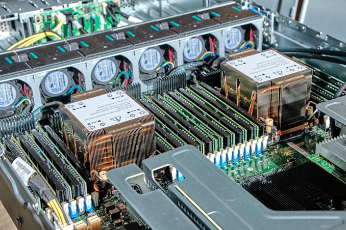
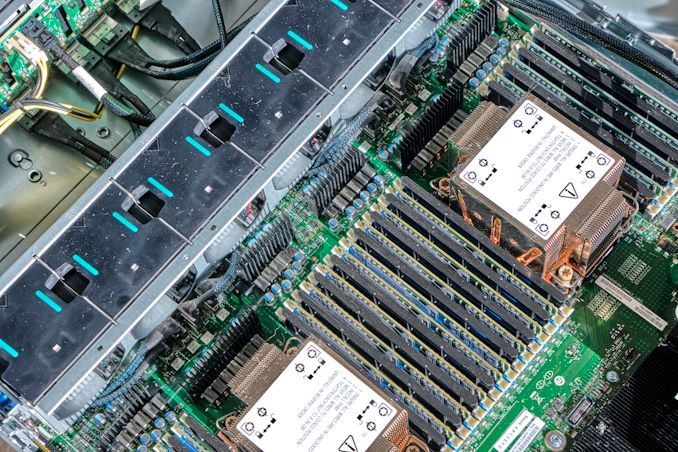
In the lead up to this launch today, Intel provided us with a 2U system featuring two of the top models of Ice Lake Xeon: we have dual 40 core Xeon Platinum 8380s! At the same time, we have also spent time a dual Xeon Gold 6330 system from Supermicro, which has two 28-core processors, and acts as a good comparison to the previous generation Xeon Platinum 8280.
Our review today will cover the processor stack, our benchmarks, power analysis, memory analysis, and some initial conclusions.
Section by Ian Cutress
Ice Lake Xeon Processor List
Intel is introducing around 40 new processors across the Xeon Platinum (8300 series), Xeon Gold (6300 and 5300 series) and Xeon Silver (4300 series). Xeon Bronze no longer exists with Ice Lake. Much like the previous generation, the 8/6/5/4 segmentation signifies the series, and the 3 indicates the generation. Beyond that the two digits are somewhat meaningless as before.
That being said, there is a significant change. In the past, Platinum/Gold/Silver also indicated socket support, with Platinum supporting up to 8P configurations. This time around, as Ice Lake does not support 8P, all the processors will support only up to 2P, with a few select models being uniprocessor only. This makes the Platinum/Gold/Silver segmentation arbitrary, if only to indicate what sort of performance/price bracket the processors are in.
On top of this, Intel is adding in more suffixes to the equation. If you work with Xeon Scalable processors day in and day out, there is now a need to differentiate the Q processor from a P processor, and an S processor from an M processor. There’s a handy list down below.
SKU List
The easiest way with this is to jump into the deep end with the processor list. RCP stands for recommended customer price, and SGX GB stands for how large Software Guard Extension enclaves can be – either 8 GB, 64 GB, or 512 GB. Cells highlighted in green show highlights in the stack.
| Intel 3rd Gen Xeon Scalable Ice Lake Xeon Only |
||||||||||
| AnandTech | Cores w/HT |
Base Freq |
1T Freq |
nT Freq |
L3 MB |
TDP W |
SGX GB |
RCP 1ku |
DC PMM |
|
| Xeon Platinum (8x DDR4-3200) | ||||||||||
| 8380 | 40 | 2300 | 3400 | 3000 | 60 | 270 | 512 | $8099 | Yes | |
| 8368 | Q | 38 | 2600 | 3700 | 3300 | 57 | 270 | 512 | $6743 | Yes |
| 8368 | 38 | 2400 | 3400 | 3200 | 57 | 270 | 512 | $6302 | Yes | |
| 8362 | 32 | 2800 | 3600 | 3500 | 48 | 265 | 64 | $5488 | Yes | |
| 8360 | Y | 36 | 2400 | 3500 | 3100 | 54 | 250 | 64 | $4702 | Yes |
| 8358 | P | 32 | 2600 | 3400 | 3200 | 48 | 240 | 8 | $3950 | Yes |
| 8358 | 32 | 2600 | 3400 | 3300 | 48 | 250 | 64 | $3950 | Yes | |
| 8352 | Y | 32 | 2200 | 3400 | 2800 | 48 | 205 | 64 | $3450 | Yes |
| 8352 | V | 36 | 2100 | 3500 | 2500 | 54 | 195 | 8 | $3450 | Yes |
| 8352 | S | 32 | 2200 | 3400 | 2800 | 48 | 205 | 512 | $4046 | Yes |
| 8352 | M | 32 | 2300 | 3500 | 2800 | 48 | 185 | 64 | $3864 | Yes |
| 8351 | N | 36 | 2400 | 3500 | 3100 | 54 | 225 | 64 | $3027 | Yes |
| Xeon Gold 6300 (8x DDR4-3200) | ||||||||||
| 6354 | 18 | 3000 | 3600 | 3600 | 39 | 205 | 64 | $2445 | Yes | |
| 6348 | 28 | 2600 | 3500 | 3400 | 42 | 235 | 64 | $3072 | Yes | |
| 6346 | 16 | 3100 | 3600 | 3600 | 36 | 205 | 64 | $2300 | Yes | |
| 6342 | 24 | 2800 | 3500 | 3300 | 36 | 230 | 64 | $2529 | Yes | |
| 6338 | T | 24 | 2100 | 3400 | 2700 | 36 | 165 | 64 | $2742 | Yes |
| 6338 | N | 32 | 2200 | 3500 | 2700 | 48 | 185 | 64 | $2795 | Yes |
| 6338 | 32 | 2000 | 3200 | 2600 | 48 | 205 | 64 | $2612 | Yes | |
| 6336 | Y | 24 | 2400 | 3600 | 3000 | 36 | 185 | 64 | $1977 | Yes |
| 6334 | 8 | 3600 | 3700 | 3600 | 18 | 165 | 64 | $2214 | Yes | |
| 6330 | N | 28 | 2200 | 3400 | 2600 | 42 | 165 | 64 | $2029 | Yes |
| 6330 | 28 | 2000 | 3100 | 2600 | 42 | 205 | 64 | $1894 | Yes | |
| 6326 | 16 | 2900 | 3500 | 3300 | 24 | 185 | 64 | $1300 | Yes | |
| 6314 | U | 32 | 2300 | 3400 | 2900 | 48 | 205 | 64 | $2600 | Yes |
| 6312 | U | 24 | 2400 | 3600 | 3100 | 36 | 185 | 64 | $1450 | Yes |
| Xeon Gold 5300 (8x DDR4-2933) | ||||||||||
| 5320 | T | 20 | 2300 | 3500 | 2900 | 30 | 150 | 64 | $1727 | Yes |
| 5320 | 26 | 2200 | 3400 | 2800 | 39 | 185 | 64 | $1555 | Yes | |
| 5318 | Y | 24 | 2100 | 3400 | 2600 | 36 | 165 | 64 | $1273 | Yes |
| 5318 | S | 24 | 2100 | 3400 | 2600 | 36 | 165 | 512 | $1667 | Yes |
| 5318 | N | 24 | 2100 | 3400 | 2700 | 36 | 150 | 64 | $1375 | Yes |
| 5317 | 12 | 3000 | 3600 | 3400 | 18 | 150 | 64 | $950 | Yes | |
| 5315 | Y | 8 | 3200 | 3600 | 3500 | 12 | 140 | 64 | $895 | Yes |
| Xeon Silver (8x DDR4-2666) | ||||||||||
| 4316 | 20 | 2300 | 3400 | 2800 | 30 | 150 | 8 | $1002 | ||
| 4314 | 16 | 2400 | 3400 | 2900 | 24 | 135 | 8 | $694 | Yes | |
| 4310 | T | 10 | 2300 | 3400 | 2900 | 15 | 105 | 8 | $555 | |
| 4310 | 12 | 2100 | 3300 | 2700 | 18 | 120 | 8 | $501 | ||
| 4309 | Y | 8 | 2800 | 3600 | 3400 | 12 | 105 | 8 | $501 | |
| Q = Liquid Cooled SKU Y = Supports Intel SST-PP 2.0 P = IaaS Cloud Specialised Processor V = SaaS Cloud Specialised Processor N = Networking/NFV Optimized M = Media Processing Optimized T = Long-Life and Extended Thermal Support U = Uniprocessor (1P Only) S = 512 GB SGX Enclave per CPU Guaranteed (...but not all 512 GB are labelled S) |
||||||||||
The peak turbo on these processors is 3.7 GHz, which is much lower than what we saw with the previous generation. Despite this, Intel seems to be keeping prices reasonable, and enabling Optane support through most of the stack except for the Silver processors (which has its own single exception).
New suffixes include Q, for a liquid cooled processor model with higher all-core frequencies at 270 W, and Intel said this part came about based on customer demand. The T processors are extended life / extended thermal support, which usually means -40ºC to 125ºC support – useful when working at the poles or in other extreme conditions. M/N/P/V specialized processors, according to our chat with Lisa Spelman, GM of the Xeon and Memory Group, are the focal points for software stack optimizations. Users that want focused hardware that can get 2-10%+ more performance on their specific workload can get these processors for which the software will be specifically tuned. Lisa stated that while all processors will receive uplifts, the segmented parts are the ones those uplifts will be targeted for. This means managing turbo vs use case and adapting code for that, which can only really be optimized for a known turbo profile.
Competition
It’s hard not to notice that the server market over the last couple of years has become more competitive. Not only is Intel competing with its own high market share, but x86 alternatives from AMD have scored big wins when it comes to per-core performance, and Arm implementations such as the Ampere Altra can enable unprecedented density at competitive performance as well. Here’s how they all stand, looking at top-of-stack offerings.
| Top-of-Stack Competition | ||||
| AnandTech | EPYC 7003 |
Amazon Graviton2 |
Ampere Altra |
Intel Xeon |
| Platform | Milan | Graviton2 | QuickSilver | Ice Lake |
| Processor | 7763 | Graviton2 | Q80-33 | 8380 |
| uArch | Zen 3 | N1 | N1 | Sunny Cove |
| Cores | 64 | 64 | 80 | 40 |
| TDP | 280 W | ? | 250 W | 270 W |
| Base Freq | 2450 | 2500 | 3300 | 2300 |
| Turbo Freq | 3500 | 2500 | 3300 | 3400 |
| All-Core | ~3200 | 2500 | 3300 | 3000 |
| L3 Cache | 256 MB | 32 MB | 32 MB | 60 MB |
| PCIe | 4.0 x128 | ? | 4.0 x128 | 4.0 x64 |
| Chipset | On CPU | ? | On CPU | External |
| DDR4 | 8 x 3200 | 8 x 3200 | 8 x 3200 | 8 x 3200 |
| DRAM Cap | 4 TB | ? | 4 TB | 4 TB |
| Optane | No | No | No | Yes |
| Price | $7890 | N/A | $4050 | $8099 |
At 40 cores, Intel does look a little behind, especially as Ampere is currently at 80 cores and a higher frequency, and will come out with a 128-core Altra Max version here very shortly. This means Ampere will be able to enable more cores in a single socket than Intel can in two sockets. Intel’s competitive advantage however will be the large current install base and decades of optimization, as well as new security features and its total offering to the market.
On a pure x86 level, AMD launched Milan only a few weeks ago, with its new Zen 3 core which has been highly impressive. Using a chiplet based approach, AMD has over 1000 mm2 of silicon to spread across 64 high performance cores and massive amounts of IO. Compared to Intel, which is around 660 mm2 and monolithic, AMD has the chipset onboard in its IO die, whereas Intel keeps it external which saves a good amount of idle power. Top of stack pricing between AMD and Intel is similar now, however AMD is also focusing in the mid-range with products like the 7F53 which really impressed us. We’ll see what Intel can respond with.
In our numbers today, we’ll be comparing Intel’s top-of-stack to everyone else. The battle royale of behemoths.
Gen on Gen Improvements: ISO Power
It is also important to look at what Intel is offering generationally in a like-for-like comparison. Intel’s 28-core 205 W point for the previous generation Cascade Lake is a good stake in the ground, and the Intel Xeon Gold 6258R is the dual socket equivalent of the Platinum 8280. We reviewed the two and they performed identically.
For this review, we’ve put the 40-core Xeon Platinum 8380 down to 205 W to see the effect of performance. But perhaps more in line, we also have the Xeon Gold 6330 which is a direct 28-core and 205 W replacement.
| Intel Xeon Comparison: 3rd Gen vs 2nd Gen 2P, 205 W vs 205 W |
|||
| Xeon Gold 6330 |
Xeon Plat 8352Y |
AnandTech | Xeon Gold 6258R |
| 28 / 56 | 32 / 64 | Cores / Threads | 28 / 56 |
| 2000 MHz Base 3100 MHz ST 2600 MHz MT |
2200 MHz Base 3400 MHz ST 2800 MHz MT |
Base Freq ST Freq MT Freq |
2700 MHz Base 4000 MHz ST 3300 MHz MT |
| 35 MB + 42 MB | 40 MB + 48 MB | L2 + L3 Cache | 28 MB + 38.5 MB |
| 205 W | 205 W | TDP | 205 W |
| PCIe 4.0 x64 | PCIe 4.0 x64 | PCIe | PCIe 3.0 x48 |
| 8 x DDR4-3200 | 8 x DDR4-3200 | DRAM Support | 6 x DDR4-2933 |
| 4 TB | 4 TB | DRAM Capacity | 1 TB |
| 200-series | 200-series | Optane | 100-series |
| 4 TB Optane + 2 TB DRAM |
4 TB Optane + 2 TB DRAM |
Optane Capacity Per Socket |
1 TB DDR4-2666 + 1.5 TB |
| 64 GB | 64 GB | SGX Enclave | None |
| 1P, 2P | 1P, 2P | Socket Support | 1P, 2P |
| 3 x 11.2 GT/s | 3x 11.2 GT/s | UPI Links | 3 x 10.4 GT/s |
| $1894 | $3450 | Price (1ku) | $3950 |
So the 6330 might seem like a natural fit, however, the 8352Y feels better given that it is more equivalent in price and offers more performance. Intel is promoting a +20% raw performance boost with the new generation, which is important here, because the 8352Y still loses 500 MHz to the previous generation in all-core frequency. The 8352Y and 6330 do make it up in the extra features, such as DDR4 channels, memory support, PCIe 4.0, Optane support, SGX enclave support, and faster UPI links.
This review has a few of our 6330 numbers that we’ve been able to run in the short time we’ve had the system.
Test Bed and Setup - Compiler Options
For the rest of our performance testing, we’re disclosing the details of the various test setups:
Intel - Dual Xeon Platinum 8380
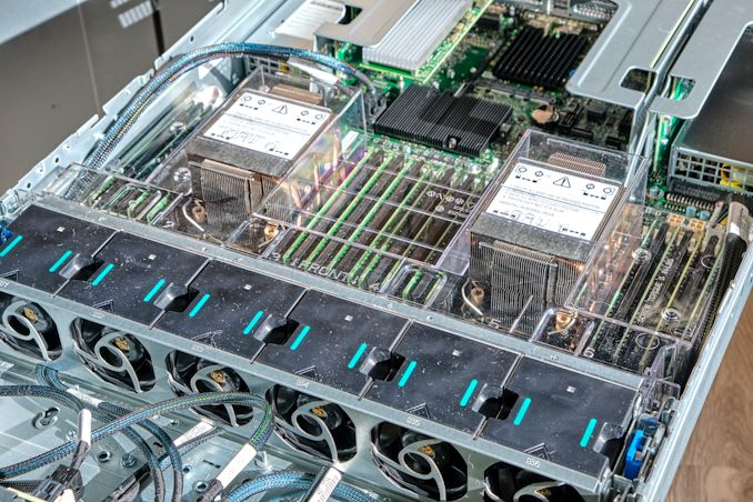
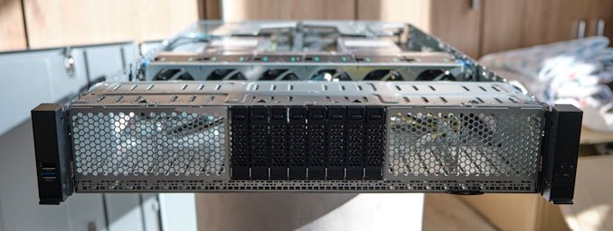
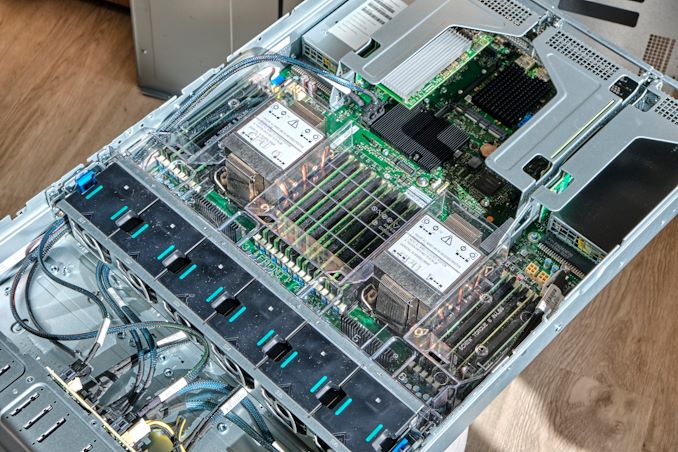
For our new Ice Lake test system based on the Whiskey Lake platform, we’re using Intel’s SDP (Software Development Platform 2SW3SIL4Q, featuring a 2-socket Intel server board (Coyote Pass).
The system is an airflow optimised 2U rack unit with otherwise little fanfare.
Our review setup solely includes the new Intel Xeon 8380 with 40 cores, 2.3GHz base clock, 3.0GHz all-core boost, and 3.4GHz peak single core boost. That’s unusual about this part as noted in the intro, it’s running at a default 205W TDP which is above what we’ve seen from previous generation non-specialised Intel SKUs.
| CPU | 2x Intel Xeon Platinum 8380 (2.3-3.4 GHz, 40c, 60MB L3, 270W) |
| RAM | 512 GB (16x32 GB) SK Hynix DDR4-3200 |
| Internal Disks | Intel SSD P5510 7.68TB |
| Motherboard | Intel Coyote Pass (Server System S2W3SIL4Q) |
| PSU | 2x Platinum 2100W |
The system came with several SSDs including Optane SSD P5800X’s, however we ran our test suite on the P5510 – not that we’re I/O affected in our current benchmarks anyhow.
As per Intel guidance, we’re using the latest BIOS available with the 270 release microcode update.
Intel - Dual Xeon Platinum 8280
For the older Cascade Lake Intel system we’re also using a test-bench setup with the same SSD and OS image as on the EPYC 7742 system.
Because the Xeons only have 6-channel memory, their maximum capacity is limited to 384GB of the same Micron memory, running at a default 2933MHz to remain in-spec with the processor’s capabilities.
| CPU | 2x Intel Xeon Platinum 8280 (2.7-4.0 GHz, 28c, 38.5MB L3, 205W) |
| RAM | 384 GB (12x32 GB) Micron DDR4-3200 (Running at 2933MHz) |
| Internal Disks | Crucial MX300 1TB |
| Motherboard | ASRock EP2C621D12 WS |
| PSU | EVGA 1600 T2 (1600W) |
The Xeon system was similarly run on BIOS defaults on an ASRock EP2C621D12 WS with the latest firmware available.
AMD - Dual EPYC 7763 / 7713 / 75F3 / 7662
In terms of testing the new EPYC 7003 series CPUs, unfortunately due to our malfunctioning Daytona server, we weren’t able to get first-hand experience with the hardware. AMD graciously gave us remote access to one of their server clusters – we had full controls of the system in terms of BMC as well as BIOS settings.
| CPU | 2x AMD EPYC 7763 (2.45-3.500 GHz, 64c, 256 MB L3, 280W) / 2x AMD EPYC 7713 (2.00-3.365 GHz, 64c, 256 MB L3, 225W) / 2x AMD EPYC 75F3 (3.20-4.000 GHz, 32c, 256 MB L3, 280W) / 2x AMD EPYC 7662 (2.00-3.300 GHz, 64c, 256 MB L3, 225W) |
| RAM | 512 GB (16x32 GB) Micron DDR4-3200 |
| Internal Disks | Varying |
| Motherboard | Daytona reference board: S5BQ |
| PSU | PWS-1200 |
Software wise, we ran Ubuntu 20.10 images with the latest release 5.11 Linux kernel. Performance settings both on the OS as well on the BIOS were left to default settings, including such things as a regular Schedutil based frequency governor and the CPUs running performance determinism mode at their respective default TDPs unless otherwise indicated.
AMD - Dual EPYC 7742
Our local AMD EPYC 7742 system, due to the aforementioned issues with the Daytona hardware, is running on a SuperMicro H11DSI Rev 2.0.
| CPU | 2x AMD EPYC 7742 (2.25-3.4 GHz, 64c, 256 MB L3, 225W) |
| RAM | 512 GB (16x32 GB) Micron DDR4-3200 |
| Internal Disks | Crucial MX300 1TB |
| Motherboard | SuperMicro H11DSI0 |
| PSU | EVGA 1600 T2 (1600W) |
As an operating system we’re using Ubuntu 20.10 with no further optimisations. In terms of BIOS settings we’re using complete defaults, including retaining the default 225W TDP of the EPYC 7742’s, as well as leaving further CPU configurables to auto, except of NPS settings where it’s we explicitly state the configuration in the results.
The system has all relevant security mitigations activated against speculative store bypass and Spectre variants.
Ampere "Mount Jade" - Dual Altra Q80-33
The Ampere Altra system we’re using the provided Mount Jade server as configured by Ampere. The system features 2 Altra Q80-33 processors within the Mount Jade DVT motherboard from Ampere.
In terms of memory, we’re using the bundled 16 DIMMs of 32GB of Samsung DDR4-3200 for a total of 512GB, 256GB per socket.
| CPU | 2x Ampere Altra Q80-33 (3.3 GHz, 80c, 32 MB L3, 250W) |
| RAM | 512 GB (16x32 GB) Samsung DDR4-3200 |
| Internal Disks | Samsung MZ-QLB960NE 960GB Samsung MZ-1LB960NE 960GB |
| Motherboard | Mount Jade DVT Reference Motherboard |
| PSU | 2000W (94%) |
The system came preinstalled with CentOS 8 and we continued usage of that OS. It’s to be noted that the server is naturally Arm SBSA compatible and thus you can run any kind of Linux distribution on it.
The only other note to make of the system is that the OS is running with 64KB pages rather than the usual 4KB pages – this either can be seen as a testing discrepancy or an advantage on the part of the Arm system given that the next page size step for x86 systems is 2MB – which isn’t feasible for general use-case testing and something deployments would have to decide to explicitly enable.
The system has all relevant security mitigations activated, including SSBS (Speculative Store Bypass Safe) against Spectre variants.
The system has all relevant security mitigations activated against the various vulnerabilities.
Compiler Setup
For compiled tests, we’re using the release version of GCC 10.2. The toolchain was compiled from scratch on both the x86 systems as well as the Altra system. We’re using shared binaries with the system’s libc libraries.
Topology, Memory Subsystem & Latency
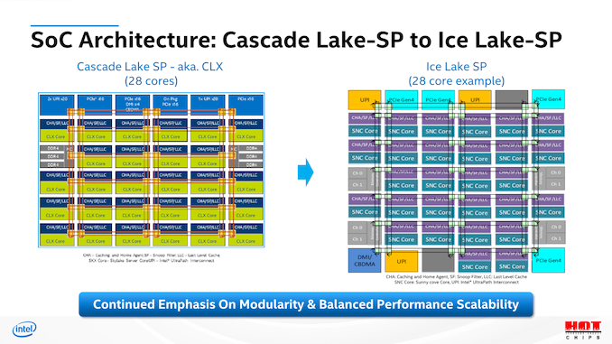
The topologies of the new Ice Lake-SP parts are quite straightforward when it comes to their generational evolution from Cascade Lake-SP. The most important thing of note here is that this generation’s HCC (high core count) die employed by Intel is of the same core count as last generation’s XCC die – 28 cores. The new ICX XCC die is now at 40 cores, with the Xeon 8380 we’re testing today being of this flavour.
Unfortunately, Intel didn’t specify which SKUs use XCC dies and which use HCC, only disclosing that XCC goes up to 40 cores, and HCC goes up to 26 cores. We also have a Xeon 6330 available for testing at 28 cores, meaning that also would be of the XCC design.
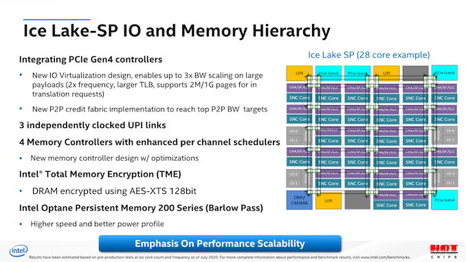
At the heart, Ice Lake SP is still a monolithic mesh design, with a few differences in the composition of the blocks, such as rearranged UPI positioning, extra 16 PCIe lanes which have been upgraded to 4.0 capability, as well as most importantly the move from a 2-memory controller design with 3-channel granularity, to a 4-controller design with 2-channel granularity, which makes for an important distinction later on in the memory performance of the system.
Starting off with our core-to-core test, the test consists of two threads atomically altering a value on a shared cache line before the threads are spawned from a main housekeeping thread. In essence we’re measuring hardware core-to-cacheline-to-core as well as the hardware coherency round-trip time for the data to be visible from one core to another. Such core-to-core latencies are important in multi-threaded workloads which have lots of shared data operations, such as databases.
At first glance, we’re not seeing all that much different latencies within a socket, however we have to remind ourselves that we’re comparing boost clocks of up to 4GHz on the Cascade Lake SP based Xeon 8280, while our Ice Lake SP Xeon 8380 only boosts up to 3.4GHz. In that regard, maintaining similar core-to-core latencies all whilst increasing the mesh size from 28 cores to 40 cores is actually quite impressive – there is a slight degradation of a few nanoseconds but generally it’s not something overly significant.
What’s a bit odd is the larger latencies between core N to core N+1 at +60ns. What’s even more odd, is that this only ever happens when we measure from physical core N to physical core N+1 on the same enumerated logical CPU, if we actually measure from physical core N to the other logical CPU of physical N+1 then we’re getting normal access latencies as any other combination of physical and logical cores. I’ve got no idea what’s happening here but the measurements seem to be consistent in their behaviour.
The major improvement on Ice Lake seems to be socket-to-socket latencies, which in our measurements have gone down from ~135ns to ~108ns on these particular SKUs at these particular frequencies. That’s a major generational improvement, and further advances Intel’s leadership position in this metric. In fact, the new Xeon 8380’s socket-to-socket latencies are now essentially the same as what AMD has to incur within a single socket between cores in different IOD quadrants, with cores within a quadrant only being slightly faster. AMD’s socket-to-socket latencies naturally fall far behind at around ~190ns, even with the newer Milan based designs which had notably improved upon this metric compared to Rome.
Memory Latency
As noted, the one big change this generation is that the CPU moves from a dual 3-channel memory controller to a quad 2-channel memory controller setup, increasing total available theoretical peak memory bandwidth by 45% through the 33% increase in memory channels, as well as the DRAM frequency increase from DDR4-2933 to DDR-3200.
Counteracting the new controller redesign is however the fact that this is simply a bigger chip, so data has to go through more mesh nodes to reach their destination as well as memory controllers.
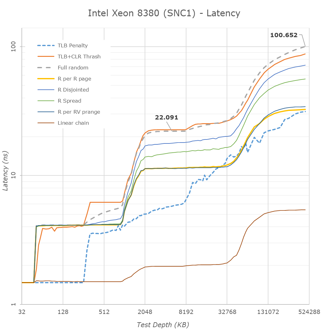
Looking at the test results with the chip in a monolithic NUMA configuration, we’re seeing the new chip slightly regress in its latencies, which actually was to be expected given the clock frequency differences between the generation SKUs. It’s not a major disadvantage, however something to keep in mind for later tests. With Intel slightly regressing, and AMD having greatly improved memory latencies in Milan, the gap between the two competitors is smaller than in previous generations where Intel had a more formidable lead.
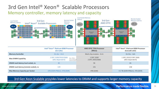
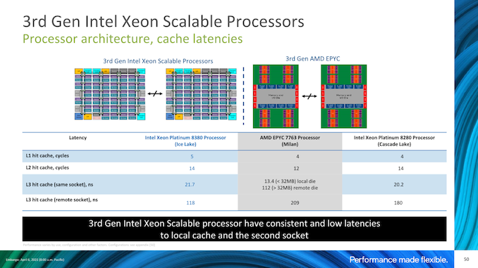
Intel’s presentations disclosed similar figures, although they’re using a different measuring methodology with MLC and simple patterns with prefetchers disabled, whereas we simply measure full random latency including TLB misses.
We weren’t able to verify the claim, but Intel also advertises advantages in remote socket DRAM latencies. The difference here matches what we’re seeing with the core-to-core latency tests, but it’s a bit of an oddball metric as I have trouble thinking of workloads where this would matter much, unless you’re running a single NUMA node across two sockets, which should be rare.
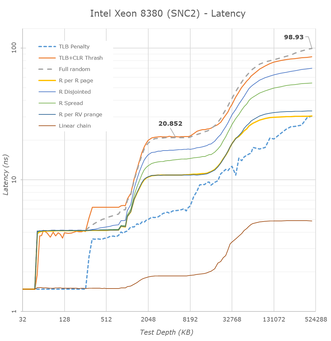
Intel had sub-NUMA clustering in prior generations, however the bigger a chip is and the larger the core count, the more these setup configurations are expected to have a difference in performance and latencies. Running the chip in SNC2 mode, meaning splitting the chip into two NUMA domains, splits the mesh into two logical parts, halving the L3 accessible to a single core, and each half only having access to their local memory controllers.
DRAM latencies here are reduced by 1.7ns, which isn’t very much a significant difference, and the L3 latencies go down by 1.2ns which is around a 5.9% reduction.
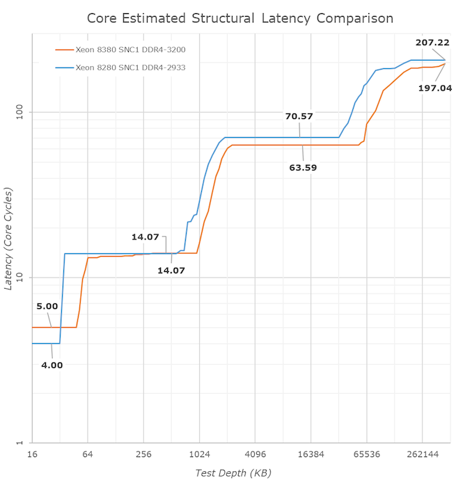
Looking at access latencies from a core cycle view, the new Ice Lake SP system is actually quite impressive. The L1 does regress from 4 to 5 cycles with the increase from 32KB to 48KB, however the L2 remains at the same 14 cycles even though it has grown from 1MB to 1.25MB.
What Intel didn’t mention in their presentation as much is that although the absolute latencies in the L3 mesh has slightly regressed from the 8280 to the new 8380, on a core clock cycle basis, it’s actually faster as we’re measuring a reduction from an average 70.5 cycles down to 63.5 cycles, which is a very impressive feat given that the mesh now contains 42% more cores, and increases its size from 38.5MB at 1.375MB/slice to 60MB at 1.5MB/slice.
Memory Bandwidth
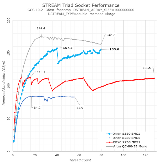
In terms of memory bandwidth, we’re falling back to the standard STREAM benchmark, in particular the Triad test which is a simple streaming memory compute test. As I had talked about more extensively in our Ampere Altra review, I find it much more interesting to test the scaling bandwidth with increasing thread count in a system as it can reveal much more nuances of system behaviour than just a simple single figure at the arbitrary maximum thread count.
We’re also using a vanilla compilation of STREAM with GCC without any explicit optimisations that alter memory operations types, as this way it’s a more realistic representation of how most generic workloads will behave on a system.
STREAM Triad is a simple test consisting of a a[j] = b[j]+scalar*c[j]; compute kernel iterating over three memory arrays. The test assumes 3 memory operations: two memory reads and one memory write. From a hardware perspective, this can actually be 4 memory operations as many cores have to first read out a content of a target cache-line before writing to it.
Generally, what we were expecting with Ice Lake SP were figures that were +45% ahead of Cascade Lake SP, thanks to the improved memory controllers and more memory channels. Instead, what we’re seeing here are improvements reaching up to +86%, well beyond the figures we were expecting.
As per the data, the new ICX design appears to be vastly outperforming its predecessor, and also essentially leaving AMD trailing far behind in terms of raw memory performance, only falling behind Ampere’s Altra which is able to dynamically detect streaming memory workloads and transform memory operations into non-temporal ones.
What’s also to be noted is that the per-core bandwidth this generation doesn’t seem to have improved very much from Cascade Lake SP, with AMD’s newest Milan still vastly outperforming Ice Lake SP at lower thread counts, and single-core bandwidth being much higher on the competitor systems.
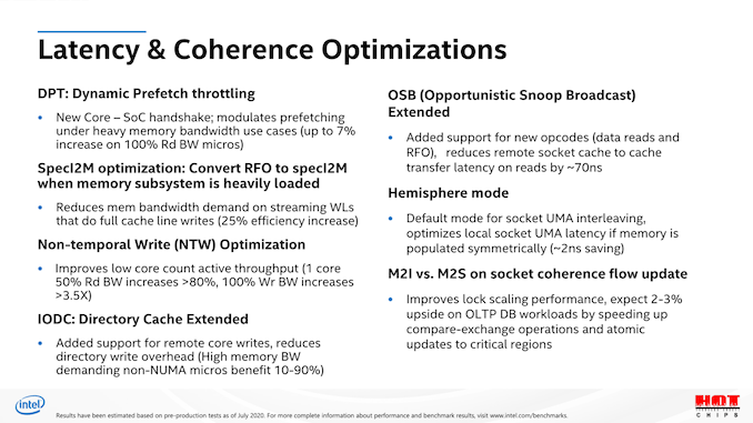
Inspecting Intel’s prior disclosures about Ice Lake SP in last year’s HotChips presentations, one point sticks out, and that is the “SpecI2M optimisation”, where the system is able to convert traditional RFO (Read for ownership) memory operations into another mechanism. We don’t know exactly what SpecI2M does, but Intel does disclose that it’s meant to optimise bandwidth and data traffic under streaming workloads. It doesn’t seem that this is a full kind of memory operation transformation into non-temporal writes as on the Arm systems we’ve seen lately, but it does significantly boost the bandwidth well beyond what we’ve seen of other x86 systems.
It’s a bit unfortunate that system vendors have ended up publishing STREAM results with hyper optimised binaries that are compiled with non-temporal instructions from the get-go, as for example we would not have seen this new mechanism on Ice Lake SP with those kind of binaries. Intel themselves are only disclosing a +47% increase in STREAM Triad performance – I consider the real-world improvement to be significantly higher than that figure, as this new dynamic mechanism doesn’t depend on specifically tuned software.
Overall, Intel’s overall larger mesh, new memory controllers, and architectural improvements in regards to memory bandwidth are absolutely impressive, and well beyond what I had expected of this generation. The latter STREAM results were really great to see as I view it as a true design innovation that will benefit a lot of workloads.
Power & Efficiency - 10nm Gains
Power efficiency in the server world infers performance, as the more efficient a CPU is, the more compute power is available in a given TDP. Ice Lake in this regard is extremely interesting given it’s Intel’s first 10nm server design, and in theory should represent a major leap forward for the new 3rd Gen Xeon line-up.
The comparison here is a bit rough this time around, as we’re dealing with a bit of a apples-and-oranges comparisons between the generational SKUs, particularly the 40-core 270W Xeon 8380 and the 28-core 205W Xeon 8280. Fortunately, we had also been sourced a Xeon 6330 from a third vendor, which is a 28-core 205W Ice Lake SP part, which should make generational comparisons a bit more interesting and fairer, although still not quite optimal as we’ll see.
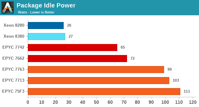
Starting off with idle package power, this was something I had made note of in our coverage of AMD’s Milan CPUs a few weeks ago, where the new AMD chip had regressed in terms of apparent IOD power and eating through the power envelope of the socket resulting in some compute performance regressions.
It’s to be noted that we’re not exactly comparing apples-to-apples here, as AMD’s designs are full SoCs, while the Intel CPUs are merely just CPUs that require the usage of an external chipset (Lewisburg Refresh) which by itself uses about 18W, essentially moving that power requirement off-socket. Intel has multiple versions of the chipset on offer, based on Compression/Encryption offload requirements, up to 28.6 W.
| Ice Lake Xeon Chipsets | ||||
| AnandTech | SKU | Compression Encryption |
RSA | TDP |
| C621A | LBG-1G | None | None | 18.0 W |
| C627A | LBG-T | 65 Gbps / 100 Gbps | 100K OPS | 28.6 W |
| C629A | LGB-C | 80 Gbps / 100 Gbps | None | 28.6 W |
Intel’s new Ice Lake SP system, similarly to the predecessor Cascade Lake SP system, appear to be very efficient at full system idle, reaching only around 27W per socket. It’s to be noted that these figures are only valid when both sockets are idle, if one socket is under load, the second socket’s power consumption will also grow in tandem even though it’s idle, we’ve seen idle figures up to 70W when the other socket is under full load, and even 90W when one socket is boosting frequencies very high. I suspect this is due to voltages and shared power delivery of the 2-socket system. Generally, it’s not of concern in the real world, but it’s just an interesting titbit to make note of.
The more interesting efficiency data is the actual power and energy consumption under load, and the corresponding performance between the generations. Again, we’re in a bit of a difficult situation here as the comparison isn’t as straightforward as the AMD Milan figures from a few weeks ago where we were comparing equal core-count and equal-TDP SKUs.
The new Xeon 8380 flagship Ice Lake SP CPU comes in at a default TDP of 270W, which is 65W higher than its direct predecessor, the 8280, and also features many more cores. Alongside the 270W default setting, I measured this part under a 205W limited power setting to add an extra data-point.
The Xeon 6330 seems a direct match to the Xeon 8280 (which in turn is identical to a Xeon 6258R), however this ICX part comes in at only $1894 versus the $3950 price point of the 6258R, a pricing that might be indicative of the quality of the silicon bin of this SKU, a point I’ll return to in just a bit.
Intel doesn’t make available core-only power metrics on its recent server chips, so we fall back to total package energy measurements only. I add in the total socket energy consumption for the duration of all workloads, as well as the performance and energy measurements on a per-thread basis as we’re dealing with different core-count designs here.
| Ice Lake-SP vs Cascade Lake-SP Power & Energy Efficiency Estimates |
|||||||||||||
| SKU | Xeon 8380 (Ice Lake-SP) |
Xeon 6330 (Ice Lake-SP) |
Xeon 8280 (Cascade Lake-SP) |
||||||||||
| TDP Setting | 270W |
205W (RAPL Limit) |
205W | 205W |
|||||||||
| Threads | 80 | 56 | |||||||||||
| Perf |
PKG (W) |
Perf | PKG (W) |
Perf | PKG (W) |
Perf | PKG (W) |
||||||
| 500.perlbench_r | 190 | 268 | 165 | 204 | 123 | 204 | 119 | 204 | |||||
| 502.gcc_r | 167 | 266 | 152 | 204 | 121 | 204 | 105 | 203 | |||||
| 505.mcf_r | 117 | 263 | 112 | 204 | 92 | 205 | 71 | 201 | |||||
| 520.omnetpp_r | 99 | 264 | 94 | 204 | 71 | 204 | 69 | 204 | |||||
| 523.xalancbmk_r | 136 | 256 | 124 | 204 | 94 | 203 | 91 | 196 | |||||
| 525.x264_r | 362 | 268 | 309 | 204 | 226 | 204 | 242 | 204 | |||||
| 531.deepsjeng_r | 163 | 268 | 140 | 204 | 101 | 204 | 107 | 205 | |||||
| 541.leela_r | 166 | 268 | 146 | 204 | 101 | 205 | 107 | 204 | |||||
| 548.exchange2_r | 290 | 269 | 248 | 204 | 178 | 205 | 170 | 205 | |||||
| 557.xz_r | 120 | 264 | 105 | 204 | 79 | 204 | 86 | 204 | |||||
| SPECint2017 est. | 167.6 | 265 | 149.1 | 204 | 111.5 | 204 | 108.4 | 203 | |||||
| kJ Total | 1937 | 1662 | 1552 | 1612 | |||||||||
| Score / W | 0.632 | 0.731 | 0.546 | 0.534 | |||||||||
| Score per Thread | 2.09 | 1.86 | 1.99 | 1.94 | |||||||||
| kJ per Thread | 24.21 | 20.78 | 27.72 | 28.78 | |||||||||
| 503.bwaves_r | 358 | 247 | 357 | 204 | 324 | 205 | 249 | 188 | |||||
| 507.cactuBSSN_r | 182 | 268 | 163 | 204 | 127 | 204 | 116 | 204 | |||||
| 508.namd_r | 194 | 268 | 164 | 204 | 122 | 204 | 127 | 205 | |||||
| 510.parest_r | 102 | 267 | 99 | 204 | 85 | 204 | 63 | 191 | |||||
| 511.povray_r | 242 | 269 | 203 | 203 | 157 | 204 | 152 | 205 | |||||
| 519.lbm_r | 38 | 236 | 38 | 204 | 34 | 199 | 26 | 173 | |||||
| 526.blender_r | 234 | 268 | 201 | 204 | 153 | 204 | 143 | 204 | |||||
| 527.cam4_r | 244 | 268 | 220 | 204 | 173 | 204 | 161 | 204 | |||||
| 538.imagick_r | 284 | 266 | 249 | 204 | 175 | 204 | 193 | 205 | |||||
| 544.nab_r | 177 | 269 | 151 | 204 | 109 | 204 | 109 | 205 | |||||
| 549.fotonik3d_r | 110 | 244 | 110 | 204 | 99 | 201 | 78 | 154 | |||||
| 554.roms_r | 78 | 261 | 78 | 204 | 68 | 205 | 50 | 173 | |||||
| SPECfp2017 est. | 160.7 | 255 | 147.4 | 204 | 118.7 | 205 | 104.8 | 184 | |||||
| kJ Total | 3877 | 3258 | 2714 | 2958 | |||||||||
| Score / W | 0.631 | 0.722 | 0.546 | 0.570 | |||||||||
| Score per Thread | 2.01 | 1.84 | 2.12 | 1.87 | |||||||||
| kJ per Thread | 48.47 | 40.73 | 48.46 | 52.82 | |||||||||
Starting off with the new flagship CPU, the Xeon 8380 indeed has little trouble to significantly outperform the Xeon 8280 by 54% in both integer and floating-point SPEC suites. This comes as no surprise as the new SKU is also using a higher TDP.
Reducing the Xeon 8380 to 205W, we’re looking at least at a performance comparison at a supposed ISO-power comparison point. Here, the Xeon 8380 again outperforms the 8280 by 40-43%. The actual measured perf/W falls in at +37% for the integer suite and +27% for the FP suite.
As per-thread performance is roughly similar between the two parts here, we can also do an energy per workload comparison, with the Ice Lake SP SKU using -27 to -23% less energy to complete the same task.
Looking at the Xeon 6330 at its default settings, the figures are quite less impressive. At +2.8 and +13.2%, the new design is posting rather lack-lustre performance boosts. The power efficiency and energy consumption figures are also extremely close to that of the 8280.
It’s to be noted, that Intel also has the Xeon 6348 in its line-up which is a 28C part as well, but with a 235W TDP. The results of the 6330 really aren’t too fantastic, even if it’s a weakly binned SKU that comes at a much cheaper price than its predecessor, meaning there’s a possible wide range in silicon quality between the new Ice Lake SKUs, indicating that a badly binned Ice Lake SKU isn’t notably better than a well binned Cascade Lake part.
SPEC - Multi-Threaded Performance
Picking up from the power efficiency discussion, let’s dive directly into the multi-threaded SPEC results. As usual, because these are not officially submitted scores to SPEC, we’re labelling the results as “estimates” as per the SPEC rules and license.
We compile the binaries with GCC 10.2 on their respective platforms, with simple -Ofast optimisation flags and relevant architecture and machine tuning flags (-march/-mtune=Neoverse-n1 ; -march/-mtune=skylake-avx512 ; -march/-mtune=znver2 (for Zen3 as well due to GCC 10.2 not having znver3).
The new Ice Lake SP parts are using the -march/-mtune=icelake-server target. It’s to be noted that I briefly tested the system with the Skylake binaries, with little differences within margin of error.
I’m limiting the detailed comparison data to the flagship SKUs, to indicate peak performance of each platform. For that reason it’s not exactly as much an architectural comparison as it’s more of a top SKU comparison.
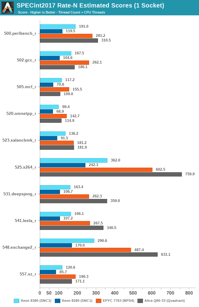
To not large surprise, the Xeon 8380 is posting very impressive performance advancements compared to the Xeon 8280, with large increases across the board for all workloads. The geo-mean increase is +54% with a low of +40% up to a high of +71%.
It’s to be noted that while the new Ice Lake system is a major generational boost, it’s nowhere near enough to catch up with the performance of the AMD Milan or Rome, or Ampere’s Altra when it comes to total throughput.
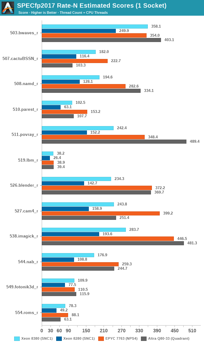
Looking at the FP suite, we have more workloads that are purely memory performance bound, and the Ice Lake Xeon 8380 again is posting significant performance increases compared to its predecessor, with a geo-mean of +53% with a range of +41% to +64%.
In some of the workloads, the new Xeon now catches up and is on par with AMD’s EPYC 7763 due to the fact that both systems have the same memory configuration with 8-channel DDR4-3200.
In any other workloads that requires more CPU compute power, the Xeon doesn’t hold up nearly as well, falling behind the competition by significant margins.
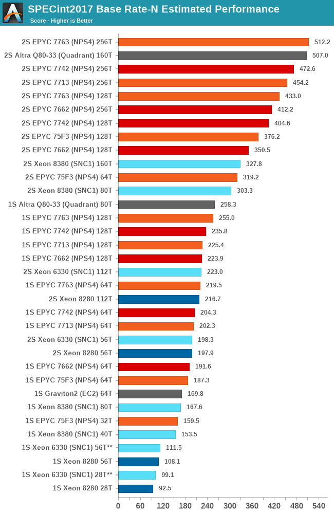
In the aggregate geomean scores, we’re seeing again that the new Xeon 8380 allows Intel to significantly reposition itself in the performance charts. Unfortunately, this is only enough to match the lower core count SKUs from the competition, as AMD and Ampere are still well ahead by massive leads – although admittedly the gap isn’t as embarrassing as it was before.
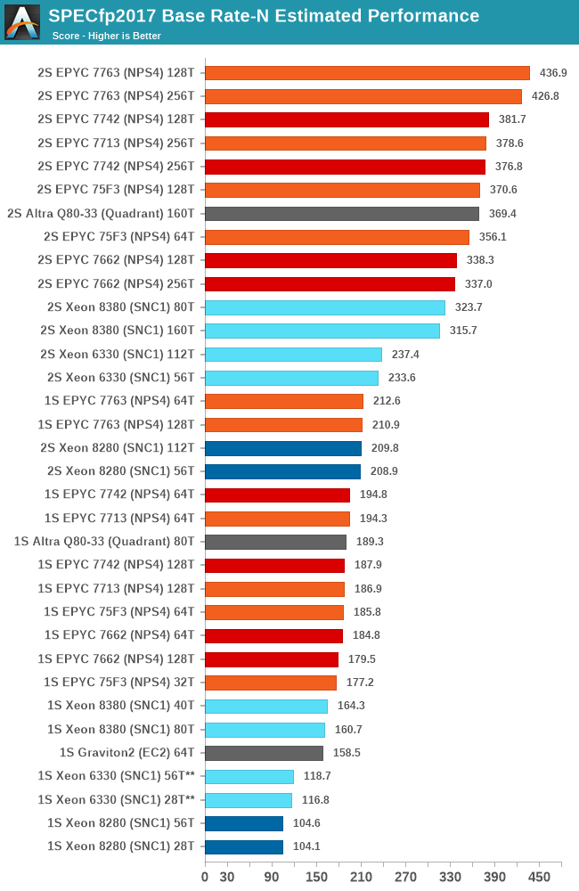
In the floating-point suite, the results are a bit more in favour for the Xeon 8380 compared to the integer suite, as the memory performance is weighed more into the total contribution of the total performance. It’s still not enough to beat the AMD and Ampere parts, but it’s much more competitive than it was before.
The Xeon 6330 is showcasing minor performance improvements over the 8280 and its cheaper equivalent the 6258R, but at least comes at half the cost – so while performance isn’t very impressive, the performance / $ might be more competitive.
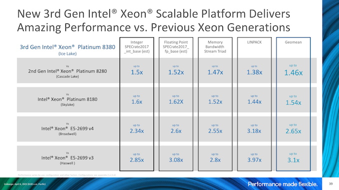
Our performance results match Intel’s own marketing materials when it comes to the generational gains, actually even surpassing Intel’s figures by a few percent.
If you would be looking at Intel’s slide above, you could be extremely enthusiastic about Intel’s new generation, as indeed the performance improvements are extremely large compared to a Cascade Lake system.
As impressive as those generational numbers are, they really only help to somewhat narrow the Grand Canyon sized competitive performance gap we’ve had to date, and the 40-core Xeon 8380 still loses out to a 32-core Milan, and from a performance / price comparison, even a premium 75F3 costs 40% less than the Xeon 8380. Lower SKUs in the Ice Lake line-up would probably fare better in perf/$, however would also just lower the performance to an even worse competitive positioning.
SPEC - Single-Threaded Performance
Single-thread performance of server CPUs usually isn’t the most important metric for most scale-out workloads, but there are use-cases such as EDA tools which are pretty much single-thread performance bound.
Power envelopes here usually don’t matter, and what is actually the performance factor that comes at play here is simply the boost clocks of the CPUs as well as the IPC improvement, and memory latency of the cores.
The one hiccup for the Xeon 8380 this generation is the fact that although there’s plenty of IPC gains to be had compared to previous microarchitectures, the new SKU is only boosting up to 3.4GHz, whereas the 8280 was able to boost up to 4GHz, which is a 15% deficit.
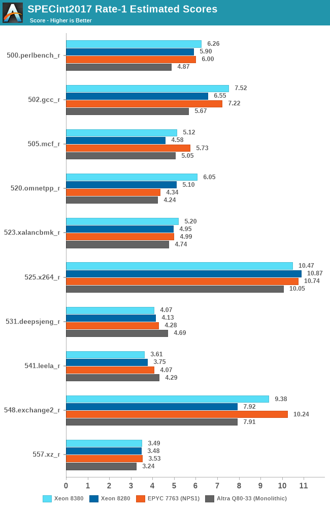
Even with the clock frequency disadvantage, thanks to the IPC gains, much improved memory bandwidth, as well as the much larger L3 cache, the new Ice Lake part to most of the time beat the Cascade Lake part, with only a couple of compute-bound core workloads where it falls behind.
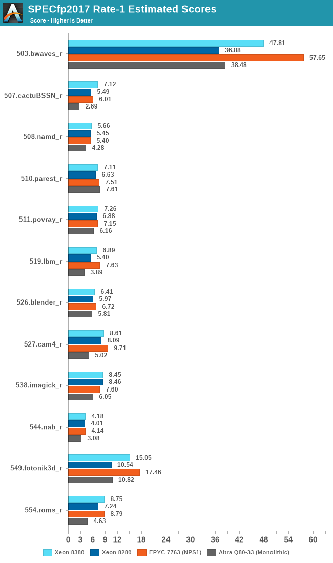
The floating-point figures are more favourable to the ICX architecture due to the stronger memory performance.
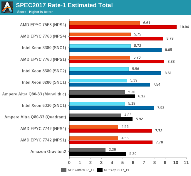
Overall, the new Xeon 8380 at least manages to post slight single-threaded performance increases this generation, with larger gains in memory-bound workloads. The 8380 is essentially on par with AMD’s 7763, and loses out to the higher frequency optimised parts.
Intel has a few SKUs which offers slightly higher ST boost clocks of up to 3.7GHz – 300Mhz / 8.8% higher than the 8380, however that part is only 8-core and features only 18MB of cache. Other SKUS offer 3.5-3.6GHz boosts, but again less cache. So while the ST figures here could improve a bit on those parts, it’s unlikely to be significant.
SPEC - Per-Core Performance under Load
A metric that is actually more interesting than isolated single-thread performance, is actually per-thread performance in a fully loaded system. This actually is a measurement and benchmark figure that would greatly interest enterprises and customers which are running software or workloads that are possibly licensed on a per-core basis, or simply workloads that require a certain level of per-thread service level agreement in terms of performance.
This has been a strong-point of Intel SKUs for some time now, even when the chips wouldn’t be competitive in terms of total throughput. With the new Ice Lake SPs SKUs now more notably increasing total throughput, it’ll be interesting to see the per-thread breakdown and resulting performance:
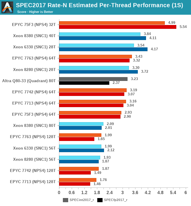
Because the total throughput generational performance increase is larger than the core count increase of the parts, this means that per-thread and per-core performance is higher with this generation. The Xeon 8380 is posting +16.3% and +10.4% per-thread performance versus the Xeon 8280 when only using one thread per core.
Interestingly, these figures are less at +8.2 and +7.4% when using both SMT threads per core. Intel has explained such an increase through the better usage of shared microarchitectural structure usage in the new Sunny Cove cores, essentially diminishing the SMT yield by improving 1/T per core performance.
Generally, Intel is extremely competitive in this benchmark metric, and while AMD easily beats them with the frequency-optimised parts, it’s an advantage that should help Intel in the SLA-centric workloads.
SPECjbb MultiJVM - Java Performance
Moving on from SPECCPU, we shift over to SPECjbb2015. SPECjbb is a from ground-up developed benchmark that aims to cover both Java performance and server-like workloads, from the SPEC website:
“The SPECjbb2015 benchmark is based on the usage model of a worldwide supermarket company with an IT infrastructure that handles a mix of point-of-sale requests, online purchases, and data-mining operations. It exercises Java 7 and higher features, using the latest data formats (XML), communication using compression, and secure messaging.
Performance metrics are provided for both pure throughput and critical throughput under service-level agreements (SLAs), with response times ranging from 10 to 100 milliseconds.”
The important thing to note here is that the workload is of a transactional nature that mostly works on the data-plane, between different Java virtual machines, and thus threads.
We’re using the MultiJVM test method where as all the benchmark components, meaning controller, server and client virtual machines are running on the same physical machine.
The JVM runtime we’re using is OpenJDK 15 on both x86 and Arm platforms, although not exactly the same sub-version, but closest we could get:
EPYC & Xeon systems:
openjdk 15 2020-09-15

OpenJDK Runtime Environment (build 15+36-Ubuntu-1)

OpenJDK 64-Bit Server VM (build 15+36-Ubuntu-1, mixed mode, sharing)
Altra system:
openjdk 15.0.1 2020-10-20

OpenJDK Runtime Environment 20.9 (build 15.0.1+9)

OpenJDK 64-Bit Server VM 20.9 (build 15.0.1+9, mixed mode, sharing)
Furthermore, we’re configuring SPECjbb’s runtime settings with the following configurables:
SPEC_OPTS_C="-Dspecjbb.group.count=$GROUP_COUNT -Dspecjbb.txi.pergroup.count=$TI_JVM_COUNT -Dspecjbb.forkjoin.workers=N -Dspecjbb.forkjoin.workers.Tier1=N -Dspecjbb.forkjoin.workers.Tier2=1 -Dspecjbb.forkjoin.workers.Tier3=16"
Where N=160 for 2S Altra test runs, N=80 for 1S Altra test runs, N=112 for 2S Xeon 8280, N=56 for 1S Xeon 8280, and N=128 for 2S and 1S on the EPYC system. The 75F3 system had the worker count reduced to 64 and 32 for 2S/1S runs.
The Xeon 8380 was running at N=140 for 2S Xeon 8380 and N=70 for 1S - the benchmark had been erroring out at higher thread counts.
In terms of JVM options, we’re limiting ourselves to bare-bone options to keep things simple and straightforward:
EPYC & Altra systems:
JAVA_OPTS_C="-server -Xms2g -Xmx2g -Xmn1536m -XX:+UseParallelGC "

JAVA_OPTS_TI="-server -Xms2g -Xmx2g -Xmn1536m -XX:+UseParallelGC"

JAVA_OPTS_BE="-server -Xms48g -Xmx48g -Xmn42g -XX:+UseParallelGC -XX:+AlwaysPreTouch"
Xeon Cascade Lake systems:
JAVA_OPTS_C="-server -Xms2g -Xmx2g -Xmn1536m -XX:+UseParallelGC"

JAVA_OPTS_TI="-server -Xms2g -Xmx2g -Xmn1536m -XX:+UseParallelGC"

JAVA_OPTS_BE="-server -Xms172g -Xmx172g -Xmn156g -XX:+UseParallelGC -XX:+AlwaysPreTouch"
Xeon Ice Lake systems (SNC1):
JAVA_OPTS_C="-server -Xms2g -Xmx2g -Xmn1536m -XX:+UseParallelGC"

JAVA_OPTS_TI="-server -Xms2g -Xmx2g -Xmn1536m -XX:+UseParallelGC"

JAVA_OPTS_BE="-server -Xms192g -Xmx192g -Xmn168g -XX:+UseParallelGC -XX:+AlwaysPreTouch"
Xeon Ice Lake systems (SNC2):
JAVA_OPTS_C="-server -Xms2g -Xmx2g -Xmn1536m -XX:+UseParallelGC"

JAVA_OPTS_TI="-server -Xms2g -Xmx2g -Xmn1536m -XX:+UseParallelGC"

JAVA_OPTS_BE="-server -Xms96g -Xmx96g -Xmn84g -XX:+UseParallelGC -XX:+AlwaysPreTouch"
The reason the Xeon CLX system is running a larger back-end heap is because we’re running a single NUMA node per socket, while for the Altra and EPYC we’re running four NUMA nodes per socket for maximised throughput, meaning for the 2S figures we have 8 backends running for the Altra and EPYC and 2 for the Xeon, and naturally half of those numbers for the 1S benchmarks.
For the Ice Lake system, I ran both SNC1 (one NUMA node) as SNC2 (two nodes), with the corresponding scaling in the back-end memory allocation.
The back-ends and transaction injectors are affinitised to their local NUMA node with numactl –cpunodebind and –membind, while the controller is called with –interleave=all.
The max-jOPS and critical-jOPS result figures are defined as follows:
"The max-jOPS is the last successful injection rate before the first failing injection rate where the reattempt also fails. For example, if during the RT-curve phase the injection rate of 80000 passes, but the next injection rate of 90000 fails on two successive attempts, then the max-jOPS would be 80000."
"The overall critical-jOPS is computed by taking the geomean of the individual critical-jOPS computed at these five SLA points, namely:
• Critical-jOPSoverall = Geo-mean of (critical-jOPS@ 10ms, 25ms, 50ms, 75ms and 100ms response time SLAs)
During the RT curve building phase the Transaction Injector measures the 99th percentile response times at each step level for all the requests (see section 9) that are considered in the metrics computations. It then computes the Critical-jOPS for each of the above five SLA points using the following formula:
(first * nOver + last * nUnder) / (nOver + nUnder) "
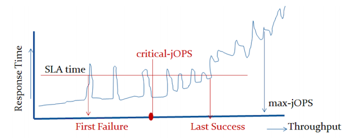
That’s a lot of technicalities to explain an admittedly complex benchmark, but the gist of it is that max-jOPS represents the maximum transaction throughput of a system until further requests fail, and critical-jOPS is an aggregate geomean transaction throughput within several levels of guaranteed response times, essentially different levels of quality of service.
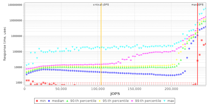
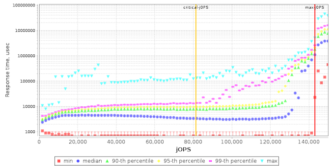
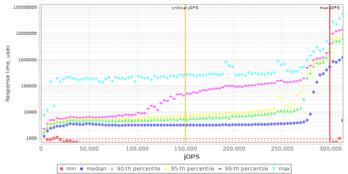
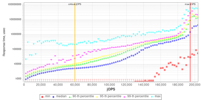
Beyond the result figures, the benchmark keeps detailed track of timings of responses and tracks a few important statistical data-points across a response-time curve, as follows:
Comparing the Xeon 8380 to the Xeon 8280, what’s to be immediately noted is the much-improved maximum throughput figure of the new part, scaling at +64% compared to its predecessor. We’re seeing that the load slope where the 99th percentile SLA figures rises comes in at a relative earlier point, and the corresponding critical-jOPS point lands in relatively earlier than the Xeon 8280.
I included the AMD EPYC 7763 and Altra graphs for context.
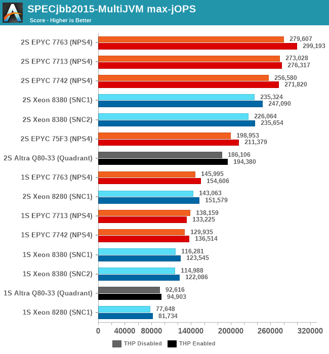
My theory here is that because of the good per-core performance of the Intel design, along with the monolithic mesh architecture, while Intel doesn’t quite catch up with AMD, it performs very well with relatively significantly fewer cores.
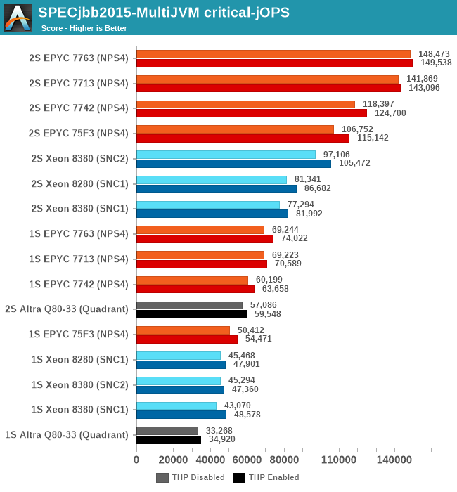
What’s really odd about the results though is that this larger increase only happens in the 2S test figures, with the 1S being unfavourable to the new Ice Lake part, losing to the 8280 in both modes. I had repeated these numbers several times to be sure they’re repeatable, and they were indeed so – as odd as that is. The 1S reduction in the critical-jOPS could be explained through the larger mesh size and larger core count of the 8380, and we did see slight regressions in core-to-core latencies. If the mesh intersection bandwidth did not increase with its size, that also could be a culprit of these figures, as the workload is hammering core-to-core transactions as well as the L3 cache of the chip.
Why the 2S figures see a bigger advantage of migrating to SNC2 could be a result of how on-chip traffic is routed, as well as the traffic flows through the UPI link blocks of the chip – at least that would be my working hypothesis.
Intel had disclosed a +62% figure for a “Java Throughput under SLA” workload they wouldn’t specify, and this does track well with our max-jOPS results. While the critical-jOPS increases seem a bit disappointing generationally, how it translates to the real world in contrast to the max-jOPS figure depends on how strict one’s SLA metrics are.
Compiling LLVM, NAMD Performance
As we’re trying to rebuild our server test suite piece by piece – and there’s still a lot of work go ahead to get a good representative “real world” set of workloads, one more highly desired benchmark amongst readers was a more realistic compilation suite. Chrome and LLVM codebases being the most requested, I landed on LLVM as it’s fairly easy to set up and straightforward.
git clone https://github.com/llvm/llvm-project.gitcd llvm-projectgit checkout release/11.xmkdir ./buildcd ..mkdir llvm-project-tmpfssudo mount -t tmpfs -o size=10G,mode=1777 tmpfs ./llvm-project-tmpfscp -r llvm-project/* llvm-project-tmpfscd ./llvm-project-tmpfs/buildcmake -G Ninja \ -DLLVM_ENABLE_PROJECTS="clang;libcxx;libcxxabi;lldb;compiler-rt;lld" \ -DCMAKE_BUILD_TYPE=Release ../llvmtime cmake --build .We’re using the LLVM 11.0.0 release as the build target version, and we’re compiling Clang, libc++abi, LLDB, Compiler-RT and LLD using GCC 10.2 (self-compiled). To avoid any concerns about I/O we’re building things on a ramdisk. We’re measuring the actual build time and don’t include the configuration phase as usually in the real world that doesn’t happen repeatedly.
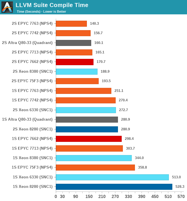
Starting off with the Xeon 8380, we’re looking at large generational improvements for the new Ice Lake SP chip. A 33-35% improvement in compile time depending on whether we’re looking at 2S or 1S figures is enough to reposition Intel’s flagship CPU in the rankings by notable amounts, finally no longer lagging behind as drastically as some of the competition.
It’s definitely not sufficient to compete with AMD and Ampere, both showcasing figures that are still 25 and 15% ahead of the Xeon 8380.
The Xeon 6330 is falling in line with where we benchmarked it in previous tests, just slightly edging out the Xeon 8280 (6258R equivalent), meaning we’re seeing minor ISO-core ISO-power generational improvements (again I have to mention that the 6330 is half the price of a 6258R).
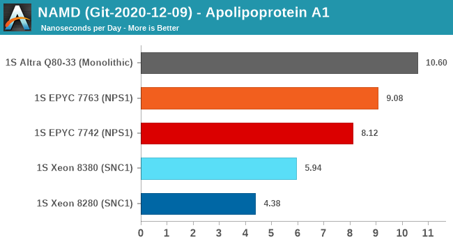
NAMD is a problem-child benchmark due to its recent addition of AVX512: the code had been contributed by Intel engineers – which isn’t exactly an issue in my view. The problem is that this is a new algorithm which has no relation to the normal code-path, which remains not as hand-optimised for AVX2, and further eyebrow raising is that it’s solely compatible with Intel’s ICC and no other compiler. That’s one level too much in terms of questionable status as a benchmark: are we benchmarking it as a general HPC-representative workload, or are we benchmarking it solely for the sake of NAMD and only NAMD performance?
We understand Intel is putting a lot of focus on these kinds of workloads that are hyper-optimised to run well extremely on Intel-only hardware, and it’s a valid optimisation path for many use-cases. I’m just questioning how representative it is of the wider market and workloads.
In any case, the GCC binaries of the test on the ApoA1 protein showcase significant performance uplifts for the Xeon 8380, showcasing a +35.6% gain. Using this apples-to-apples code path, it’s still quite behind the competition which scales the performance much higher thanks to more cores.
Conclusion & End Remarks
Today’s launch of the new 3rd gen Xeon Scalable processors is a major step forward for Intel and the company’s roadmap. Ice Lake SP had been baking in the oven for a very long time: originally planned for a 2020 release, Intel had only started production recently this January, so finally seeing the chips in silicon and in hand has been a relief.
Generationally Impressive
Technically, Ice Lake SP is an impressive and major generation leap for Intel’s enterprise line-up. Manufactured on a new 10nm process, node, employing a new core microarchitecture, faster memory with more memory channels, PCIe 4.0, new accelerator capabilities and VNNI instructions, security improvements – these are all just the tip of the iceberg that Ice Lake SP brings to the table.
In terms of generational performance uplifts, we saw some major progress today with the new Xeon 8380. With 40 cores at a higher TDP of 270W, the new flagship chip is a veritable beast with large increases in performance in almost all workloads. Major architectural improvements such as the new memory bandwidth optimisations are amongst what I found to be most impressive for the new parts, showcasing that Intel still has a few tricks up its sleeve in terms of design.
This being the first super-large 10nm chip design from Intel, the question of how efficiency would end up was a big question to the whole puzzle to the new generation line-up. On the Xeon 8380, a 40-core part at 270W, we saw a +18% increase in performance / W compared to the 28-core 205W Xeon 8280. This grew to a +36% perf/W advantage when limiting the ICX part to 205 as well. On the other hand, our mid-stack Xeon 6330 sample showed very little advantages to the Xeon 8280, even both are 28-core 205W designs. Due to the mix of good and bad results here, it seems we’ll have to delay a definitive verdict on the process node improvements to the future until we can get more SKUs, as the current variations are quite large.
Per-core performance, as well as single-thread performance of the new parts don’t quite achieve what I imagine Intel would have hoped through just the IPC gains of the design. The IPC gains are there and they’re notable, however the new parts also lose out on frequency, meaning the actual performance doesn’t move too much, although we did see smaller increases. Interestingly enough, this is roughly the same conclusion we came to when we tested Intel's Ice Lake notebook platform back in August 2019.
The Competitive Hurdle Still Stands
As impressive as the new Xeon 8380 is from a generational and technical stand-point, what really matters at the end of the day is how it fares up to the competition. I’ll be blunt here; nobody really expected the new ICL-SP parts to beat AMD or the new Arm competition – and it didn’t. The competitive gap had been so gigantic, with silly scenarios such as where competing 1-socket systems would outperform Intel’s 2-socket solutions. Ice Lake SP gets rid of those more embarrassing situations, and narrows the performance gap significantly, however the gap still remains, and is still undeniable.
We’ve only had access limited to the flagship Xeon 8380 and the mid-stack Xeon 6330 for the review today, however in a competitive landscape, both those chips lose out in both absolute performance as well as price/performance compared to AMD’s line-up.
Intel had been pushing very hard the software optimisation side of things, trying to differentiate themselves as well as novel technologies such as PMem (Optane DC persistent memory, essentially Optane memory modules), which unfortunately didn’t have enough time to cover for this piece. Indeed, we saw a larger focus on “whole system solutions” which take advantage of Intel’s broader product portfolio strengths in the enterprise market. The push for the new accelerator technologies means Intel needs to be working closely with partners and optimising public codebases to take advantage of these non-standard solutions, which might be a hurdle for deployments such as cloud services where interoperability might be important. While the theoretical gains can be large, anyone rolling a custom local software stack might see a limited benefit however, unless they are already experts with Intel's accelerator portfolio.
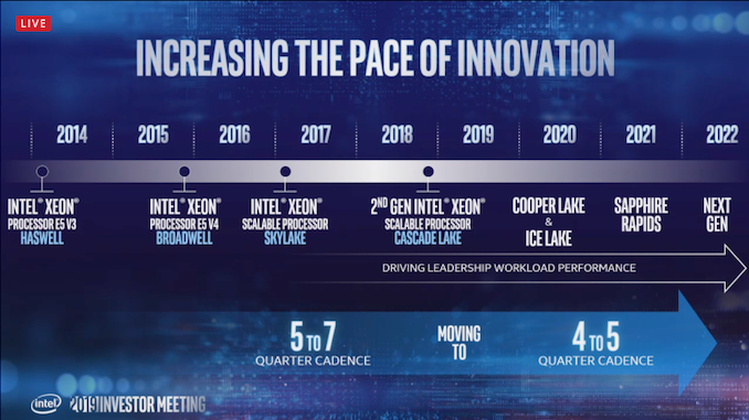
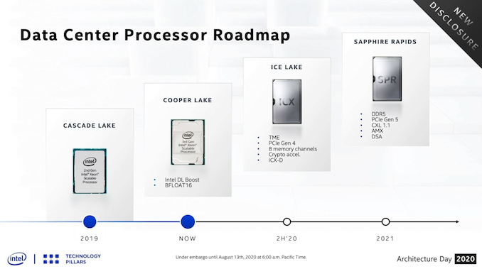
There’s also the looming Intel roadmap. While we are exulted to finally see Ice lake SP reach the market, Intel is promising the upcoming Sapphire Rapids chips for later this year, on a new platform with DDR5 and PCIe 5. Intel is set to have Ice Lake Xeon and Sapphire Rapids Xeon in the market concurrently, with the idea to manage both, especially for customers that apply the leading edge hardware as soon as it is available. It will be interesting to see the scale of the roll out of Ice Lake with this in mind.
At the end of the day, Ice Lake SP is a success. Performance is up, and performance per watt is up. I'm sure if we were able to test Intel's acceleration enhancements more thoroughly, we would be able to corroborate some of the results and hype that Intel wants to generate around its product. But even as a success, it’s not a traditional competitive success. The generational improvements are there and they are large, and as long as Intel is the market share leader, this should translate into upgraded systems and deployments throughout the enterprise industry. Intel is still in a tough competitive situation overall with the high quality the rest of the market is enabling.

