Original Link: https://www.anandtech.com/show/163
| When turning on the TV, there is a good chance you'll be able to catch a new car commercial within 30 seconds of flipping stations. It seems like for every new model of a car that is released, there is always a revolutionary redesign that took place to bring you what you see in front of your eyes today. In many cases, that revolutionary redesign is nothing more than a fix for problems which shouldn't have been present in the first revolutionary design, however there are some cases where tweaking an existing product and marketing it as a revamped design is truthful. When we do happen to come by such a case it is often difficult judging how effective the improvements to the original design were, in the case of a car it's often quite noticeable, however with a microprocessor for example, evaluating the improvements can be a bit more complicated. |  |
| Case in point would be AMD's newly released 400MHz K6-2. Unlike previously released K6-2 processors such as the 333 and the 350 which offered only an increased clock speed over their predecessors, the K6-2 400 boasts a "new and improved" core (sound familiar?) which supposedly improves the overall performance of the processor, in addition to the obviously increased clock speed over the older K6-2 350. | |
Before the processor's November 16 announcement at Fall Comdex '98, there was much speculation as to what the "new and improved" core actually meant from both an engineering and a real world usage perspective. In the end, it took a little more than a few benchmarks to reveal what AMD worked into the K6-2 400, however the results looked quite promising.
The K6-2 400 will probably be the last K6-2 processor of the year, and therefore the last K6-2 processor to ever leave AMD's fabrication plants as their K6-3 is planned for an early Q1 launch in 1999. It is always a good thing to leave any situation with a memorial bang, and as the industry has shown us time and time again, such an exit is possible. ABIT gave the old Intel 430HX chipset a just farewell with their revamped IT5H Revision 2.0, and let's see if AMD can show the K6-2 processor a proper good-bye before it shoves off into retirement with the revamped K6-2 400.
The K6-2 400 starts off as a chip based on the same original design that the 266, 300, 333, and 350MHz parts sprouted from. A processor that is pin compatible with the Socket-7 CPU interface, albeit a Super7 processor requiring official support for the 100MHz FSB in order to perform at its peak. The K6-2 400, like all others in its slowly ending family, boasts support for AMD's own batch of 3DNow! instructions designed to improve mathematical calculations, specifically those involved in 3D games which take advantage of the added instructions. The chip itself has a full 64KB of L1 cache, and has no on-chip L2 cache, a feature that is reserved for the upcoming K6-3 aka "Sharptooth" processor. However that is where the similarities end, and the improvements begin to kick in with the K6-2 400.
Stepping to the beat of a different drummer
The K6-2 is now available in a few new models or steppings as they are commonly referred to in the microprocessor industry. AMD just recently released three new additions to the K6-2 processor family, the K6-2 366, 380, and 400. The 366 and 380MHz parts are labeled Model 8/[7:0] as will all newer 350MHz parts, however the 400MHz unit is marked as a Model 8/[F:8] to indicate the use of AMD's new CXT core.
There have been reports of newer 350MHz parts with the newly improved core found in the 400MHz part, while older 350MHZ K6-2's are making use of the more common core found in the 7:0 processors...but what are the differences between these two processor revisions?
New Clock Multipliers
According to AMD's specifications, the K6-2 400 (Model 8/[F:8]) translates the 2.0x clock multiplier into a 6.0x clock multiplier as is defined by the below found in the AMD processor documentation
| State of BF[2:0] Inputs | Processor-Clock to Bus-Clock Ratio |
| 100b | 2.5x |
| 101b | 3.0x |
| 110b | 2.0x or 6.0x |
| 111b | 3.5x |
| 000b | 4.5x |
| 001b | 5.0x |
| 010b | 4.0x |
| 011b | 5.5x |
| The ratio selected is dependent on the stepping of the Model 8. The 2.0x ratio is supported on the Model 8/[7:0], whereas the 6.0x ratio is supported on the Model 8/[F:8]. | |
What does this mean? It basically indicates that stepping 7:0 of the model 8 K6-2 processor supports clock multipliers ranging from 2.0x - 5.5x, whereas stepping F:8 supports clock multipliers ranging from 2.5x - 6.0x, with the 2.0x setting corresponding to a 6.0x clock multiplier.
Why on earth would we need a 6.0x clock multiplier? For users that don't have Super7 motherboards, the K6-2 400 is still capable of running on your system, albeit considerably slower, at 66MHz x 6.0 instead of forcing it to run at 66MHz x 5.5. You'll begin to see more K6-2 overdrive type processors using the K6-2 400 as they can make use of the 6.0x clock multiplier to get the processor to work on motherboards that only support the 66MHz FSB.
Intolerable Heat
In addition to the new clock multiplier present in the F:8 chip, the 400MHz K6-2 also has a lower tolerance for an operating case temperature under maximum thermal power in comparison to previous parts, including other model 8 processors. Where the K6-2 350, 366, and 380MHz parts will allow for an ambient case temperature in the 00C–700C range, the 400MHz part is a bit more sensitive only allowing for a 00C–600C range. While this may not seem like a big problem considering your case shouldn't be in that range, in AnandTech's tests, the K6-2 400 seemed to be much more sensitive to thermal fluctuation than the K6-2 350 or 333. Some of that sensitivity can be attributed to the fact that AnandTech tested an engineering sample of the processor, however overall, you can expect the K6-2 400 to be a bit more sensitive to heat than its predecessors.
Write Handling Control Register
If you remember back to the release of the original AMD K6, one of the performance enhancing features that needed to be supported by motherboard manufacturers in their BIOS's on K6 compliant boards was "Write Allocate." Write allocate is a feature of the K6 architecture that allows the processor to cache a memory write that isn't already located within the L1 data cache. Using a burst read to fetch the data located outside the L1 cached region, a write allocate will store the data from the memory write in the processor's L1 data cache. Although the performance of a single write allocate function isn't greater than if the data were written to memory had a burst read not taken place, the real benefit of write allocate is visible in writes to the write allocated cache line after the initial write allocate. This is because the probability that a memory write will occur closer to a previous write is greater than a memory write occurring in an area far away from the previous write. Eventually, you'll experience a performance gain from using multiple write allocates in comparison to forgoing the burst read cycles and allowing the memory writes to complete without write allocate intervention.
Write allocate can be triggered via one [or more] of three methods that indicate an "eligible" memory write is taking place: Write to a Cacheable Page, Write to a Sector, and Write Allocate Limit. The main difference between the two steppings of the model 8 K6-2 discussed here occurs in the usage of the Write Allocate Limit method. The Write Allocate Limit is enabled by what is known as the Write Handling Control Register, or WHCR for short.
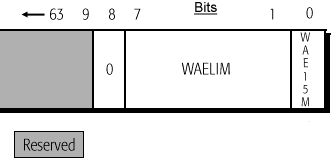
In stepping 7:0 of K6-2 processors, the WHCR is composed of three fields: the WCDE bit, the Write Allocate Enable Limit (WAELIM) field, and the Write Allocate Enable 15-to-16Mbyte (WAE15M) bit as described by the following figure taken from AMD's K6-2 400 documentation:

Stepping F:8 changes the picture slightly, with the WHCR composed of two fields: the Write Allocate Enable Limit (WAELIM) field, and the Write Allocate Enable 15-to-16Mbyte (WAE15M) bit as described by the following figure taken from AMD's K6-2 400 documentation:

One thing you'll notice is that the WAELIM field is larger in the second diagram (10 bits wide - Model 8/[F:8]) in comparison to the first diagram (7 bits wide - Model 8/[7:0]). This indicates that the theoretical limit for Write Allocates to take place in the F:8 stepping has been raised from 508MB of memory to 4096MB as was the case with older processors. Once again, we have been given a feature that really won't effect us that much, however the real performance increase comes from the next enhancement which somewhat walks hand in hand with Write Allocate.
Write Merge Buffer
Where Write Allocate fails, the K6-2's (Model 8/[F:8]) 8-byte Write Merge Buffer picks up. Instead of simply leaving non-cacheable write cycles alone, the Write Merge Buffer combines the data segments from all a group of memory writes into this 8-byte buffer. By combining all of the writes into the Write Merge Buffer, you can theoretically reduce processor bus utilization and processor stalls, which accounts for the overall increase in performance the newer F:8 stepping offers over the older processors.
The Test & Taking Advantage
How can you take advantage of the improvements found in the new CXT core? Unfortunately it isn't as simple as popping in a new chip, you will have to make an update to your BIOS to recognize the processor as well as to enable the enhanced WHCR and the Write Merge Buffer. As you'll be able to see from the tests AnandTech conducted, the K6-2 400 using the CXT core exhibited a 7% increase in overall performance in comparison to a K6-2 400 without the modifications enabled in the WHCR and with the Write Merge Buffer. As far as gaming performance goes, the K6-2 400 doesn't really benefit all that much from the Write Merge Buffer, although you may see a few fps increase in performance in a few of your games, nothing too major.
The Socket-7/Super7 Test System Configuration was as follows:
AMD K6-2 350, AMD K6-2 400 CXT
FIC VA-503+ Motherboard w/ special BIOS update
64MB PC100 SDRAM
Western Digital Caviar AC35100 - UltraATA
Matrox Millennium G200 AGP Video Card (8MB)
The Pentium II comparison system differed only in terms of the processor and motherboard in which case the following components were used:
Intel Celeron 300A, Intel Pentium II 400
ABIT BX6 Pentium II BX Motherboard
The Pentium II Xeon comparison system differed only in terms of the processor and motherboard in which case the following components were used:
Intel Xeon 400/1MB
Supermicro S2DGU GX Motherboard
The following drivers were common to both test systems:
MGA G200 Drivers v1677_426
DirectX 6
All tests were run at 1024 x 768 x 16-bit color

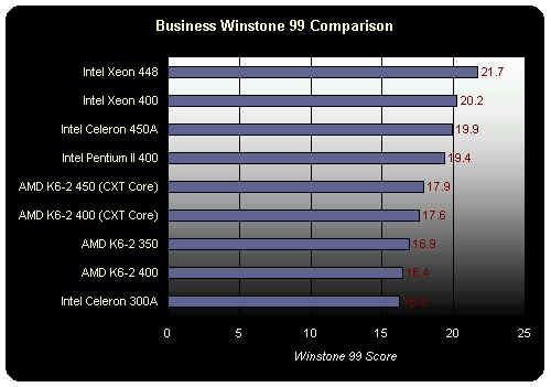
If you'll notice, without BIOS support, the K6-2 400 CXT is actually slower than a K6-2 350 without the core improvements. However, once you enable the Write Merge Buffer and allow the WHCR modifications to take place, the picture does change considerably. One interesting thing to note is that under Winstone 99, Intel processors score considerably higher than their Super7 counterparts. This is primarily because Winstone 99 centers itself around multitasking performance, where the Pentium II, Celeron, and Xeon processors excel. Since their L2 cache runs at a much higher speed than that of the K6-2, they allow the multiple applications, which fit almost entirely in the L2 cache, to perform much better than those that run on Super7 platforms where the L2 cache is limited to run at 100MHz (without overclocking that is).
Speaking of overclocking, the K6-2 400 engineering sample AnandTech received wasn't the world's most stable overclocker, however you can realistically expect to be able to overclock the 400MHz parts to at least 450MHz, unfortunately it seems as if 500MHz may be pushing it unless you get a chip from a very good batch.
Tying up the loose ends
With everything described, and the improvements explained, in the end, is the K6-2 400 a better solution than the Pentium II 400? It all depends on price. The K6-2 400 is a strong performer, and as long as the cost of the K6-2 400 system remains below that of a Pentium II 400 system, the K6-2 will be the better option, simply because AMD has already guaranteed and shown us (see the Comdex updates) a true upgrade path for the K6-2, the K6-3. Provided that the K6-3 ships on time, any Super7 purchase now will be fully upgradable to a K6-3 next year, not too bad of an insurance package. Although Intel's upcoming Katmai, which is due for release sometime in late Q2 of 1999, will be a Slot-1 processor, chances are that you'll want to opt for Intel's upcoming Camino chipset to make use of all of the functionality of that processor so a Katmai upgrade won't be the most economical justification for a Slot-1 system now. If AMD can keep the prices of the K6-2 400, at least equal to or below that of a Celeron 300A (which can usually be overclocked to 450MHz) then the choice isn't too difficult to make. Unfortunately, you'll also have to deal with the wonderful Super7 compatibility issues when it comes to video cards...but we'll save that for another day.


