Original Link: https://www.anandtech.com/show/16214/amd-zen-3-ryzen-deep-dive-review-5950x-5900x-5800x-and-5700x-tested
AMD Zen 3 Ryzen Deep Dive Review: 5950X, 5900X, 5800X and 5600X Tested
by Dr. Ian Cutress on November 5, 2020 9:01 AM EST
When AMD announced that its new Zen 3 core was a ground-up redesign and offered complete performance leadership, we had to ask them to confirm if that’s exactly what they said. Despite being less than 10% the size of Intel, and very close to folding as a company in 2015, the bets that AMD made in that timeframe with its next generation Zen microarchitecture and Ryzen designs are now coming to fruition. Zen 3 and the new Ryzen 5000 processors, for the desktop market, are the realization of those goals: not only performance per watt and performance per dollar leaders, but absolute performance leadership in every segment. We’ve gone into the new microarchitecture and tested the new processors. AMD is the new king, and we have the data to show it.
New Core, Same 7nm, Over 5.0 GHz!
The new Ryzen 5000 processors are drop-in replacements for the Ryzen 3000 series. Anyone with an AMD X570 or B550 motherboard today, with the latest BIOS (AGESA 1081 or above), should be able to buy and use one of the new processors without a fuss. Anyone with an X470/B450 board will have to wait until Q1 2021 as those boards are updated.
As we’ve previously covered, AMD is launching four processors today for retail, ranging from six cores up to sixteen cores.
| AMD Ryzen 5000 Series Processors Zen 3 Microarchitecture |
||||||
| AnandTech | Cores Threads |
Base Freq |
Turbo Freq |
L3 Cache |
TDP | MSRP |
| Ryzen 9 5950X | 16c/32t | 3400 | 4900 | 64 MB | 105 W | $799 |
| Ryzen 9 5900X | 12c/24t | 3700 | 4800 | 64 MB | 105 W | $549 |
| Ryzen 7 5800X | 8c/16t | 3800 | 4700 | 32 MB | 105 W | $449 |
| Ryzen 5 5600X | 6c/12t | 3700 | 4600 | 32 MB | 65 W | $299* |
*Comes with Bundled CPU Cooler
All the processors have native support for DDR4-3200 memory as per JEDEC standards, although AMD recommends something slightly faster for optimum performance. All the processors also have 20 lanes of PCIe 4.0 for add-in devices.
The Ryzen 9 5950X: 16 Cores at $799
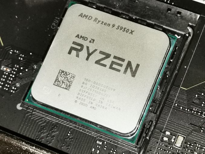
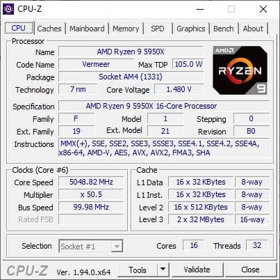
The top processor is the Ryzen 9 5950X, with 16 cores and 32 threads, offering a base frequency of 3400 MHz and a turbo frequency of 4900 MHz – on our retail processor, we actually detected a single core frequency of 5050 MHz, indicating that this processor will turbo above 5.0 GHz with sufficient thermal headroom and cooling!
This processor is enabled through two eight core chiplets (more on chiplets below), each with 32 MB of L3 cache (total 64 MB). The Ryzen 9 5950X is rated at the same TDP as the Ryzen 9 3950X, at 105 W. The peak power will be ~142 W, as per AMD’s socket design, on motherboards that can support it.
For those that don’t read the rest of the review, the short conclusion for the Ryzen 9 5950X is that even at $799 suggested retail price, it enables a new level of consumer grade performance across the board. The single thread frequency is crazy high, and when combined with the new core design with its higher IPC, pushes workloads that are single-core limited above and beyond Intel’s best Tiger Lake processors. When it comes to multi-threaded workloads, we have new records for a consumer processor across the board.
The Ryzen 9 5900X: 12 Cores at $549
Squaring off against Intel’s best consumer grade processor is the Ryzen 9 5900X, with 12 cores and 24 threads, offering a base frequency of 3700 MHz and a turbo frequency of 4800 MHz (4950 MHz was observed). This processor is enabled through two six-core chiplets, but all the cache is still enabled at 32 MB per chiplet (64 MB total). The 5900X also has the same TDP as the 3900X/3900XT it replaces at 105 W.
At $549, it is priced $50 higher than the processor it replaces, which means that for the extra 10% cost it will have to showcase that it can perform at least 10% better.
The Ryzen 7 5800X: 8 Cores at $449
After AMD showcased a quad core processor under $100 in the last generation, it takes a lot of chutzpah to offer an eight core processor for $449 – AMD stands by its claims that this processor offers substantial generational performance improvements. The new AMD Ryzen 7 5800X, with eight cores and sixteen threads, is set to go up against Intel’s Core i7-10700K, also an eight core / sixteen thread processor.
The Ryzen 7 5800X has a base frequency of 3800 MHz and a rated turbo frequency of 4700 MHz (we detected 4825 MHz), and uses a single eight-core chiplet with a total 32 MB of L3 cache. The single core chiplet has some small benefits over a dual chiplet design where some cross-CPU communication is needed, and that comes across in some of our very CPU-limited gaming benchmarks. This processor also has 105 W TDP (~142 W peak).
The Ryzen 5 5600X: 6 Cores for $299
The cheapest processor that AMD is releasing today is the Ryzen 5 5600X, but it is also the only one that comes with a CPU cooler in box. The Ryzen 5 5600X has six cores and twelve threads, running at a base frequency of 3700 MHz and a peak turbo of 4600 MHz (4650 MHz measured), and is the only CPU to be given a TDP of 65 W (~88 W peak).
The single chiplet design means 32 MB of L3 cache total (technically it’s still the same that a single core can access as the Ryzen 9 parts, more on that later), and will be put up against Intel’s six-core Core i5-10600K, which also retails in a similar ballpark.
Despite being the cheapest and technically the slowest processor of the bunch, I was mightily surprised by the performance of the Ryzen 5 5600X: similar to the Ryzen 9 5950X, in single threaded benchmarks, it completely knocks the socks off of anything Intel has to offer – even Tiger Lake.
Why Ryzen 5000 Works: Chiplets
At a high level, the new Ryzen 5000 'Vermeer' series seem oddly familiar to the last generation Ryzen 3000 ‘Matisse’ series. This is actually by design, as AMD is fully leveraging their chiplet design methodology in the new processors.
To introduce some terminology, AMD creates two types of chiplets. One of them has the main processing cores, and is called a core complex die or CCD. This is the one that is built on TSMC's 7nm process. The other chiplet is an interconnect die with I/O, known as an IO die or IOD - this one has the PCIe lanes, the memory controllers, the SATA ports, the connection to the chipset, and helps control power delivery as well as security. In both the previous generation and the new generation, AMD pairs one of its IO dies with up to two 8-core chiplets.
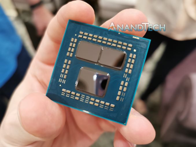
Ryzen 3000 processor without heatspreader, showing two core chiplets and one IO die.
This is possible because the new core chiplets contain the same protocols for interconnect, physical design, and power constraints. AMD is able to leverage the execution of the previous platform and generation such that when the core connections are identical, despite the different internal structures (Zen 3 vs Zen 2), they can still be put together and executed in a known and successful fashion.
As with the previous generation, the new Zen 3 chiplet is designed with eight cores
Zen 3 is a New Core Design
By keeping the new 8-core Zen 3 chiplet the same size and same power, this obviously means that AMD had to build a core that fits within those constraints but also affords a performance and performance efficiency uplift in order to make a more compelling design. Typically when designing a CPU core, the easiest thing to do is to take the previous design and upgrade certain parts of it – or what engineers call tackling ‘the low hanging fruit’ which enables the most speed-up for the least effort. Because CPU core designs are built to a deadline, there are always ideas that never make it into the final design, but those become the easiest targets for the next generation. This is what we saw with Zen 1/Zen+ moving on to Zen 2. So naturally, the easiest thing for AMD to do would be the same again, but with Zen 3.
However, AMD did not do this. In our interviews with AMD’s senior staff, we have known that AMD has two independent CPU core design teams that aim to leapfrog each other as they build newer, high performance cores. Zen 1 and Zen 2 were products from the first core design team, and now Zen 3 is the product from the second design team. Naturally we then expect Zen 4 to be the next generation of Zen 3, with ‘the low hanging fruit’ taken care of.
In our recent interview with AMD’s Chief Technology Officer, Mark Papermaster, we were told that if you were to look at the core from a 100,000 foot level, you might easily mistake that the Zen 3 core design to be similar to that of Zen 2. However, we were told that because this is a new team, every segment of the core has been redesigned, or at the very least, updated. Users who follow this space closely will remember that the branch predictor used in Zen 2 wasn’t meant to come until Zen 3, showing that even the core designs have an element of portability to them. The fact that both Zen 2 and Zen 3 are built on the same TSMC N7 process node (the same PDK, although Zen 3 has the latest yield/consistency manufacturing updates from TMSC) also helps in that design portability.
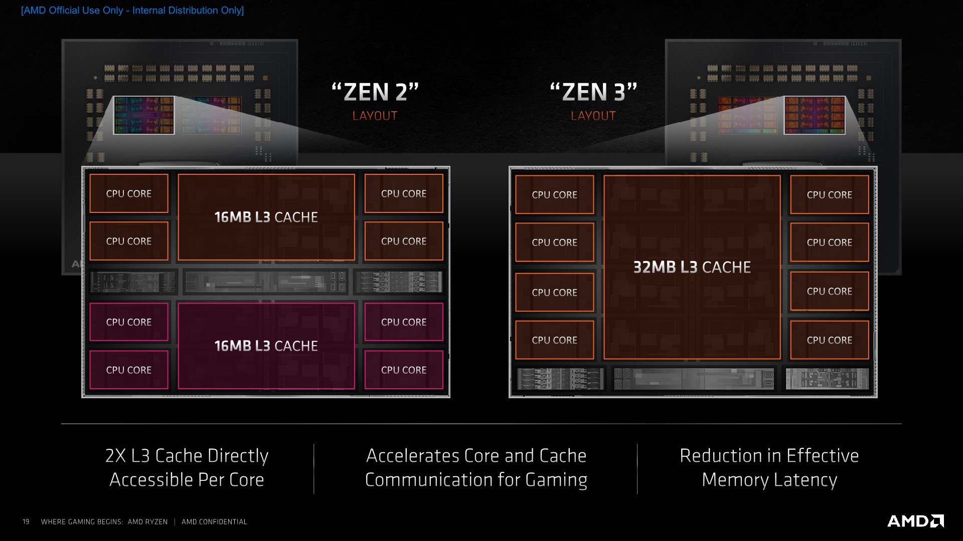
AMD has already announced the major change that will be obvious to most of the techies that are interested in this space: the base core chiplet, rather than having two four-core complexes, has a single eight-core complex. This enables each core to access the whole 32 MB of L3 cache of a die, rather than 16 MB, which reduces latency of memory accesses in that 16-to-32 MB window. It also simplifies core-to-core communication within a chiplet. There are a couple of trade-offs to do this, but overall it is a good win.
In fact there are a significant number of differences throughout the core. AMD has improved:
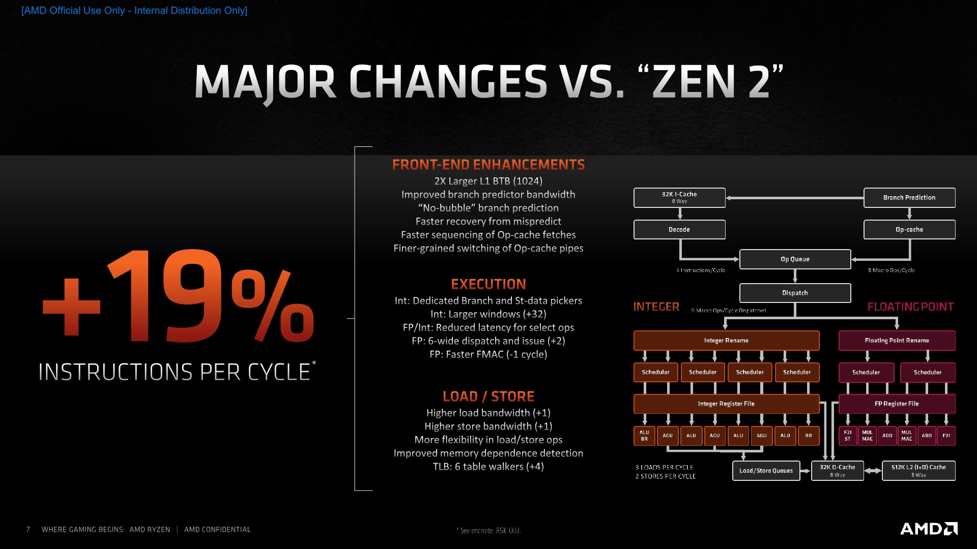
- branch prediction bandwidth
- faster switching from the decode pipes to the micro-op cache,
- faster recoveries from mispredicts,
- enhanced decode skip detection for some NOPs/zeroing idioms
- larger buffers and execution windows up and down the core,
- dedicated branch pipes,
- better balancing of logic and address generation,
- wider INT/FP dispatch,
- higher load bandwidth,
- higher store bandwidth,
- better flexibility in load/store ops
- faster FMACs
- A wide variety of faster operations (including x87?)
- more TLB table walkers
- better prediction of store-to-load forward dependencies
- faster copy of short strings
- more AVX2 support (VAES, VPCLMULQD)
- substantially faster DIV/IDIV support
- hardware acceleration of PDEP/PEXT
Many of these will be explained and expanded upon over the next few pages, and observed in the benchmark results. Simply put, this is something more than just a core update – these are genuinely new cores and new designs that required new sheets of paper to be built upon.
A number of these features, such as wider buffers and increased bandwidth, naturally come with the question about how AMD has kept the power the same for Zen 3 compared to Zen 2. Normally when a core gets wider, that means more silicon has to be turned on all the time, and this influences static power, or if it all gets used simultaneously, then there is higher active power.
When speaking with Mark Papermaster, he pointed to AMD’s prowess in physical implementation as a key factor in this. By leveraging their knowledge of TSMC’s 7nm (N7) process, as well as updates to their own tools to get the best out of these designs, AMD was able to remain power neutral, despite all this updates and upgrades. Part of this also comes from AMD’s long standing premium partner relationship with TMSC, being able to enable better design technology co-optimization (DTCO) between floorplan, manufacturing, and product.
AMD’s Claims
The CPU marketing teams from AMD, since the launch of first generation Zen, have been very accurate in their performance claims, even to the point of understating performance from time to time. Aside from promoting performance leadership in single thread, multi-thread, and gaming, AMD promoted several metrics for generation-on-generation improvement.
+19% IPC
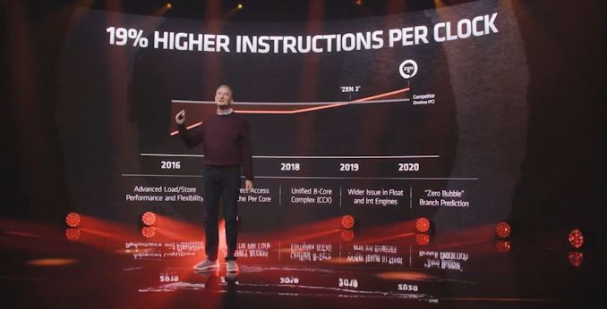
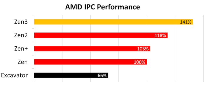
The key metric offered by AMD was a +19% IPC uplift from Zen 2 to Zen 3, or rather a +19% uplift from Ryzen 5 3800XT to Ryzen 5 5800X when both CPUs are at 4.0 GHz and using DDR4-3600 memory.
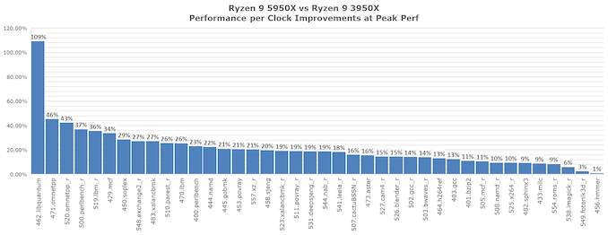
In fact, using our industry benchmarks, for single threaded performance, we observed a +19% increase in CPU performance per clock. We have to offer kudos to AMD here, this is the second or third time they've quoted IPC figures which we've matched.
In multithreaded SPECrate, the absolute gain was only around 10% or so, given that faster cores also require more bandwidth to main memory, which hasn’t been provided in this generation. This means that there are some bottlenecks to which a higher IPC won’t help if more cores require the same resources.
For real-world tests, across our whole suite, we saw an average +24% uplift. For explicitly multithreaded tests, we saw ranges from even performance up to +35%, while for explicitly single threaded tests, this ranged from even performance up to +57%. This comes down to execution/compute bound tests getting bigger speedups over memory bound workloads.
Best Gaming
For gaming, the number was given as a +5 to +50% uplift in 1920x1080 gaming at the high preset, comparing a Ryzen 9 5900X against the Ryzen 9 3900XT, depending on the benchmark.
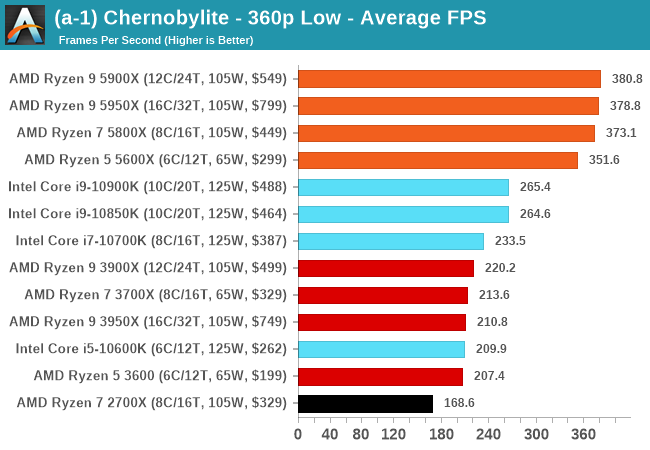
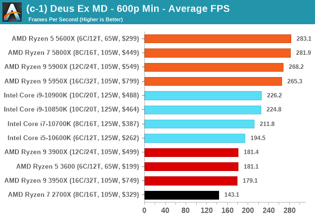
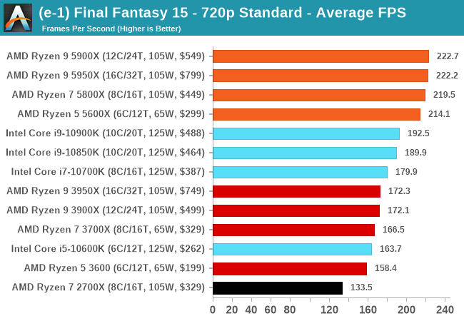
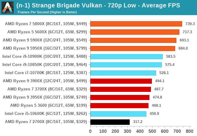
In our tests at CPU limited settings, such as 720p or 480p minimum, we saw an average +44% frames-per-second performance uplift comparing the Ryzen 9 5950X to the Ryzen 9 3950X. Depending on the test, this ranged from +10% to +80% performance uplift, with key gains in Chernobylite, Borderlands 3, Gears Tactics, and F1 2019.
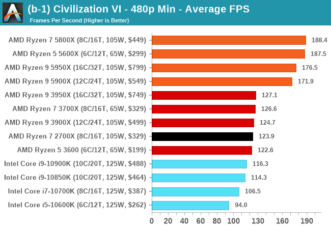
For our more mainstream gaming tests, run at 1920x1080 with all the quality settings on maximum, the performance gain averaged around +10%. This spanned the gamut from an equal score (World of Tanks, Strange Brigade, Red Dead Redemption), up to +36% (Civilization 6, Far Cry 5).
Perhaps the most important comparison is the AMD Ryzen 9 5950X against the Intel Core i9-10900K. In our CPU limited tests, we get a +21% average FPS win for the AMD at CPU-limited scenarios, ranging from +2% to +52%. But in our 1080p Maximum settings tests, the results were on average neck-and-neck, swaying from -4% to +6%. (That result doesn’t include the one anomaly in our tests, as Civilization 6 shows a +43% win for AMD.)
Head-to-Head Performance Matchups
Based on core counts and pricing, the new Ryzen 5000 series processors closely align with some of Intel’s most popular Comet Lake processors, as well as the previous generation AMD hardware.
| Q4 2020 Matchups | ||||||
| AMD Ryzen 5000 |
Cores | SEP | Tray 1ku |
Cores | Intel Core 10th Gen |
|
| Ryzen 9 5950X | 16C | $799 | vs. | $999 | 18C | Core i9-10980XE* |
| Ryzen 9 5900X | 12C | $549 | vs. | $488 | 10C | Core i9-10900K |
| Ryzen 7 5800X | 8C | $449 | vs. | $453 | 10C | Core i9-10850K |
| $374 | 8C | Core i7-10700K | ||||
| Ryzen 5 5600X | 6C | $299 | vs. | $262 | 6C | Core i5-10600K |
*Technically a high-end desktop platform processor, almost unavailable at MSRP.
Throughout this review we will be referencing these comparisons, and will eventually break-out each processor into its own analysis breakdown.
More In This Review
As this is our Deep Dive coverage into Zen 3, we are going to go into some nitty-gritty details. Over the next few pages, we will go over:
- Improvements to the core design (prefetchers, buffers, execution units, etc)
- Our microbenchmark tests (core-to-core latency, cache hierarchy, turbo ramping)
- New Instructions, Improved instructions
- SoC Power and Per-Core Power
- SPEC2006 and SPEC2017 results
- CPU Benchmarks (Office, Science, Simulation, Rendering, Encoding, Web, Legacy)
- Gaming Benchmarks (11 tests, 4 settings per test, with RTX 2080 Ti)
- Conclusions and Final Remarks
Section by Andrei Frumusanu
The New Zen 3 Core: High-Level
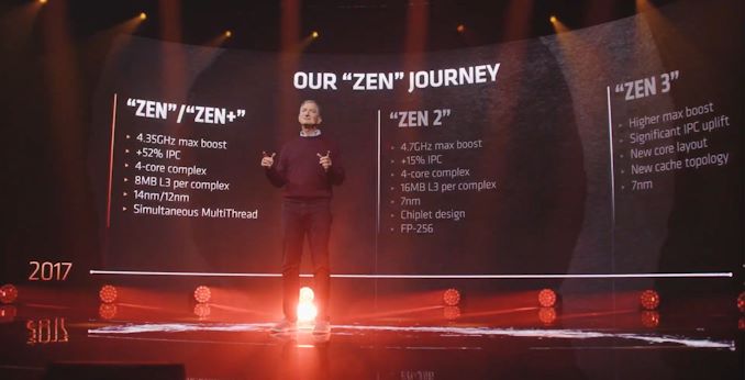
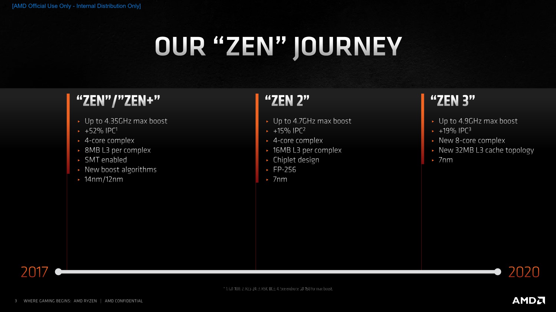
As we dive into the Zen3 microarchitecture, AMD made a note of their journey of the last couple of years, a success-story that’s been started off in 2017 with the revolutionary Zen architecture that helped bring AMD back to the competitive landscape after several sombre years of ailing products.
The original Zen architecture brought a massive 52% IPC uplift thanks to a new clean-sheet microarchitecture which brought at lot of new features to the table for AMD, introducing features such as a µOP cache and SMT for the first time into the company’s designs, as well as introducing the notion of CPU core-complexes with large (8MB at the time) L3 caches. Features on a 14nm FinFET process node, it was the culmination and the start-off point of a new roadmap of microarchitectures which leads into today’s Zen3 design.
Following a minor refresh in the form of Zen+, last year’s 2019 Zen2 microarchitecture was deployed into the Ryzen 3000 products, which furthered AMD’s success in the competitive landscape. Zen2 was what AMD calls a derivative of the original Zen designs, however it contained historically more changes than what you’d expect from such a design, bringing more IPC increases than what you’d typically see. AMD saw Zen2 as a follow-up to what they had learned with the original Zen microarchitecture, fixing and rolling out design goal changes that they had initially intended for the first design, but weren’t able to deploy in time for the planned product launch window. AMD also stated that it enabled an opportunity to bring some of the future Zen3 specific changes were moved forward into the Zen2 design.
This was also the point at which AMD moved to the new chiplet design, leveraging the transition to TSMC’s new 7nm process node to increase the transistor budget for things like doubling the L3 cache size, increasing clock speeds, and vastly reducing the power consumption of the product to enable aggressive ramp in total core counts both in the consumer space (16-core Ryzen 9 3950X), as well as in the enterprise space (64-core EPYC2 Rome).
Tying a cutting-edge high-performance 7nm core-complex-die (CCD) with a lower cost 12/14nm I/O die (IOD) in such a heterogenous package allowed AMD to maximise the advantages and minimise the disadvantages of both respective technologies – all whilst AMD’s main competitor, Intel, was, and still is, struggling to bring out 10nm products to the market. It was a technological gamble that AMD many times has said was made years in advance, and has since paid off plenty.
Zen 3 At A Glance
This brings us to today’s Zen3 microarchitecture and the new Ryzen 5000 series. As noted earlier, Mark Papermaster had mentioned that if you were to actually look at the new design from a 100,000-foot level, you’d notice that it does look extremely similar to previous generation Zen microarchitectures. In truth, while Zen3 does share similarities to its predecessors, AMD’s architects started off with a clean-sheet design, or as they call it – “a ground-up redesign”. This is actually quite a large claim as this is a quite enormous endeavour to venture in for any company. Arm’s Cortex-A76 is the most recent other industry design that is said to have been designed from scratch, leveraging years of learning of the different design teams and solving inherent issues that require more invasive and large changes to the design.
Because the new Zen3 core still exhibits quite a few defining characteristics of the previous generation designs, I think that AMD’s take on a “complete redesign” is more akin to a deconstruction and reconstruction of the core’s building blocks, much like you’d dismantle a LEGO set and rebuild it anew. In this case, Zen3 seems to be a set-piece both with new building blocks, but also leveraging set pieces and RTL that they’ve used before in Zen2.
Whatever the interpretation of a “clean-sheet” or “complete redesign” might be, the important take is that Zen3 is a major overhaul in terms of its complete microarchitecture, with AMD paying attention to every piece of the puzzle and trying to bring balance to the whole resulting end-design, which comes in contrast to a more traditional “derivative design” which might only touch and see changes in a couple of the microarchitecture’s building blocks.
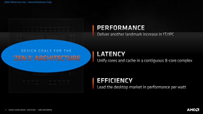
AMD’s main design goals for Zen3 hovered around three main points:
- Delivering another significant generational single-threaded performance increase. AMD did not want to be relegated to top performance only in scenarios where workloads would be spread across all the cores. The company wanted to catch up and be an undisputed leader in this area to be able to claim an uncontested position in the market.
- Latency improvements, both in terms of memory latency, achieved through a reduction in effective memory latency through more cache-hits thanks to the doubled 32MB L3 that an individual core can take advantage of, as well as core-to-core latency which again thanks to the consolidated single L3 cache on the die is able to reduce long travel times across the dies.
- Continuing a power efficiency leadership: Although the new Zen3 cores still use the same base N7 process node from TSMC (although with incremental design improvements), AMD had a constraint of not increasing power consumption for the platform. This means that any new performance increases would have to come through simultaneous power efficiency improvements of the microarchitecture.
The culmination of all the design changes AMD has made with the Zen3 micro-architecture results in what the company claims as a 19% average performance uplift over a variety of workloads. We’ll be breaking down this number further into the review, but internal figures show we are matching the 19% average uplift across all SPEC workloads, with a median figure of 21%. That is indeed a tremendous achievement, considering the fact that the new Ryzen 5000 chips clock slightly higher than their predecessors, further amplifying the total performance increase of the new design.
Section by Andrei Frumusanu
The New Zen 3 Core: Front-End Updates
Moving on, let’s see what makes the Zen3 microarchitecture tick and how detail on how it actually improves things compared to its predecessor design, starting off with the front-end of the core which includes branch prediction, decode, the OP-cache path and instruction cache, and the dispatch stage.
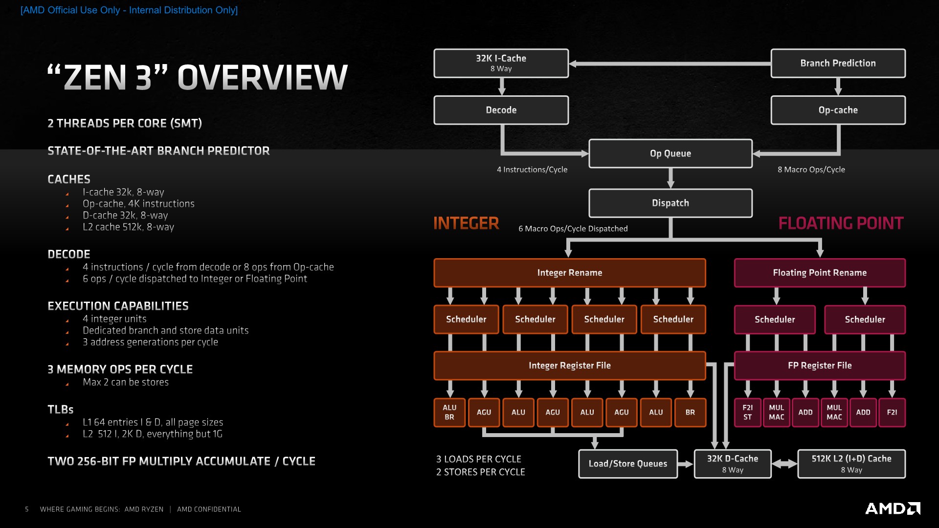
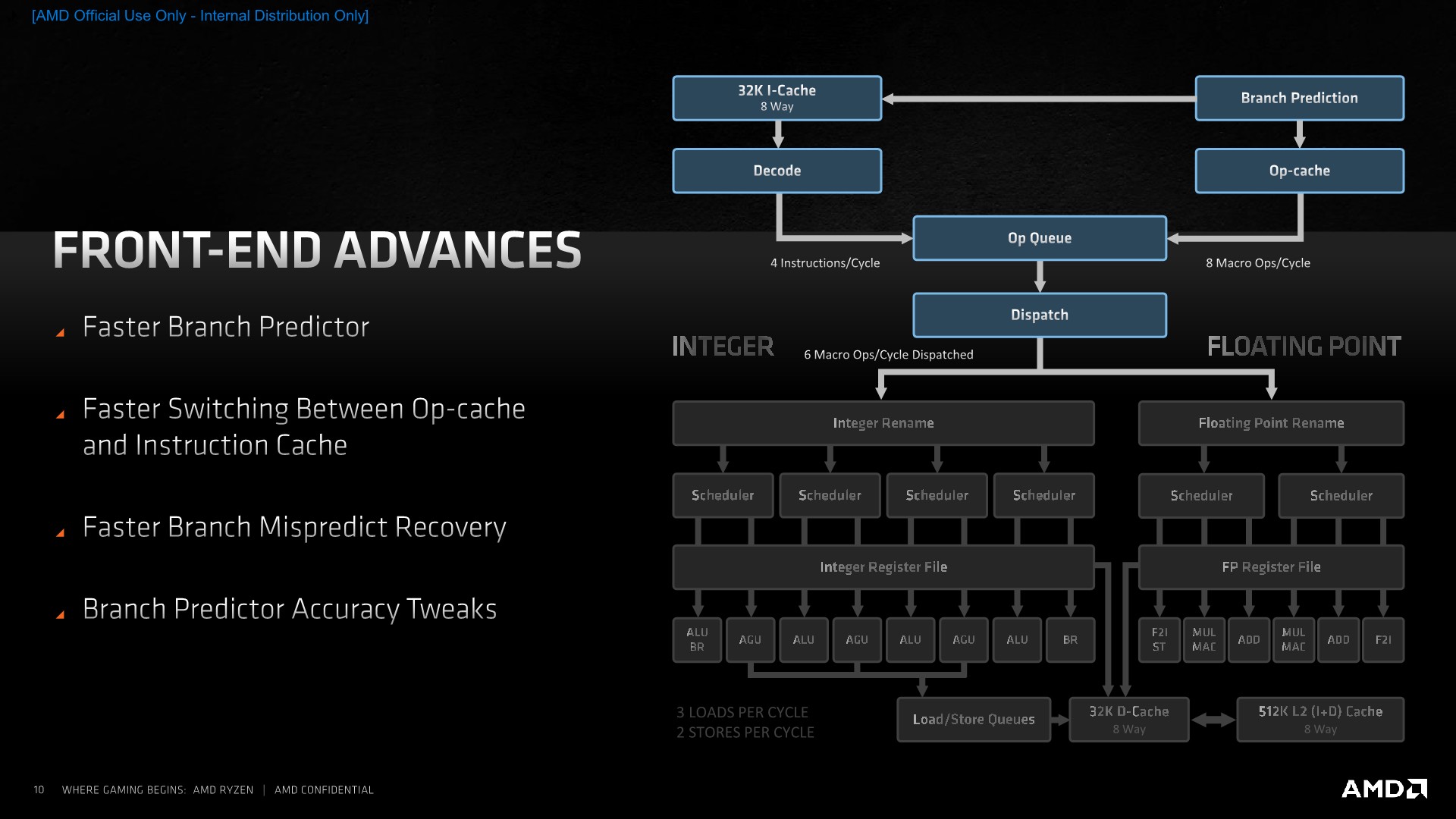
From a high-level overview, Zen3’s front-end looks the same as on Zen2, at least from a block-diagram perspective. The fundamental building blocks are the same, starting off with the branch-predictor unit which AMD calls state-of-the-art. This feeds into a 32KB instruction cache which forwards instructions into a 4-wide decode block. We’re still maintaining a two-way flow into the OP-queue, as when we see instructions again which have been previously decoded, they are then stored in the OP-cache from which they can be retrieved with a greater bandwidth (8 Mops/cycle) and with less power consumption.
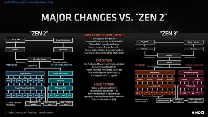
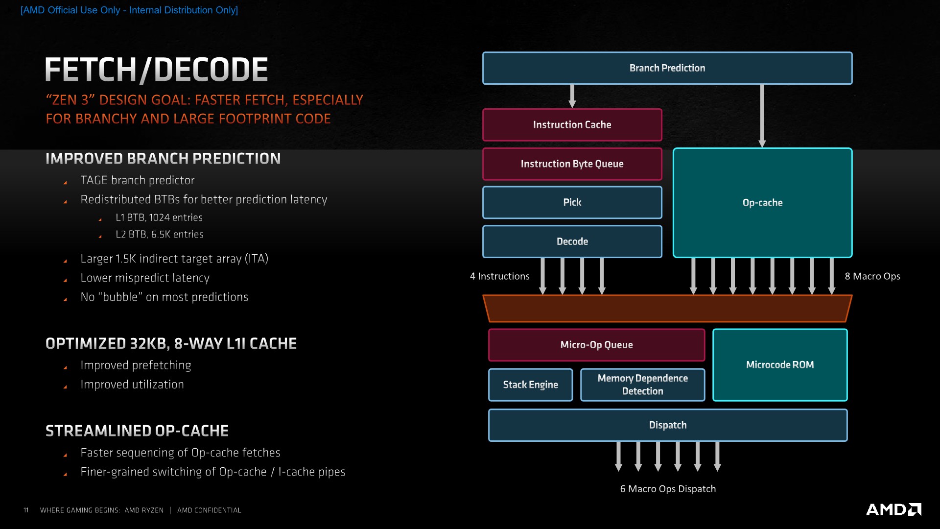
Improvements of the Zen3 cores in the actual blocks here include a faster branch predictor which is able to predict more branches per cycle. AMD wouldn’t exactly detail what this means but we suspect that this could allude to now two branch predictions per cycle instead of just one. This is still a TAGE based design as had been introduced in Zen2, and AMD does say that it has been able to improve the accuracy of the predictor.
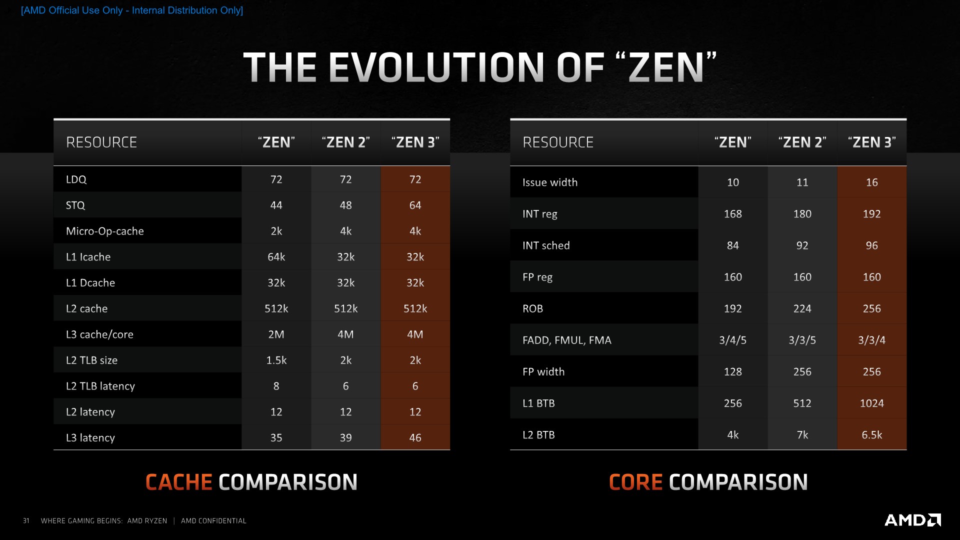
Amongst the branch unit structure changes, we’ve seen a rebalancing of the BTBs, with the L1 BTB now doubling in size from 512 to 1024 entries. The L2 BTB has seen a slight reduction from 7K to 6.5K entries, but allowed the structure to be more efficient. The indirect target array (ITA) has also seen a more substantial increase from 1024 to 1536 entries.
If there is a misprediction, the new design reduces the cycle latency required to get a new stream going. AMD wouldn’t exactly detail the exact absolute misprediction cycles or how faster it is in this generation, but it would be a more significant performance boost to the overall design if the misprediction penalty is indeed reduced this generation.
AMD claims no bubbles on most predictions due to the increased branch predictor bandwidth, here I can see parallels to what Arm had introduced with the Cortex-A77, where a similar doubled-up branch predictor bandwidth would be able to run ahead of subsequent pipelines stages and thus fill bubble gaps ahead of them hitting the execution stages and potentially stalling the core.
On the side of the instruction cache, we didn’t see a change in the size of the structure as it’s still a 32KB 8-way block, however AMD has improved its utilisation. Prefetchers are now said to be more efficient and aggressive in actually pulling data out of the L2 ahead of them being used in the L1. We don’t know exactly what kind of pattern AMD alludes to having improved here, but if the L1I behaves the same as the L1D, then adjacent cache lines would then be pulled into the L1I here as well. The part of having a better utilisation wasn’t clear in terms of details and AMD wasn’t willing to divulge more, but we suspect a new cache line replacement policy to be a key aspect of this new improvement.
Being an x86 core, one of the difficulties of the ISA is the fact that instructions are of a variable length with encoding varying from 1 byte to 15 bytes. This has been legacy side-effect of the continuous extensions to the instruction set over the decades, and as modern CPU microarchitectures become wider in their execution throughput, it had become an issue for architects to design efficient wide decoders. For Zen3, AMD opted to remain with a 4-wide design, as going wider would have meant additional pipeline cycles which would have reduced the performance of the whole design.
Bypassing the decode stage through a structure such as the Op-cache is nowadays the preferred method to solve this issue, with the first-generation Zen microarchitecture being the first AMD design to implement such a block. However, such a design also brings problems, such as one set of instructions residing in the instruction cache, and its target residing in the OP-cache, again whose target might again be found in the instruction cache. AMD found this to be a quite large inefficiency in Zen2, and thus evolved the design to better handle instruction flows from both the I-cache and the OP-cache and to deliver them into the µOP-queue. AMD’s researchers seem to have published a more in-depth paper addressing the improvements.
On the dispatch side, Zen3 remains a 6-wide machine, emitting up to 6-Macro-Ops per cycle to the execution units, meaning that the maximum IPC of the core remains at 6. The Op-cache being able to deliver 8 Macro-Ops into the µOp-queue would serve as a mechanism to further reduce pipeline bubbles in the front-end – as the full 8-wide width of that structure wouldn’t be hit at all times.
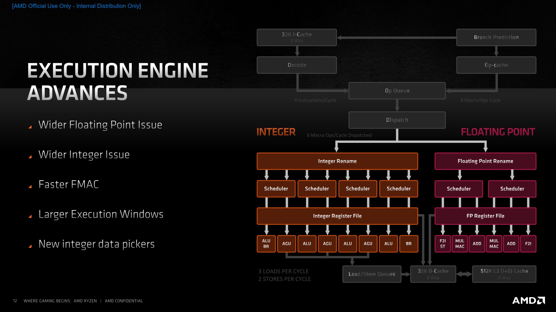
On the execution engine side of things, we’ve seen a larger overhaul of the design as the Zen3 core has seen a widening of both the integer and floating-point issue width, with larger execution windows and lower latency execution units.
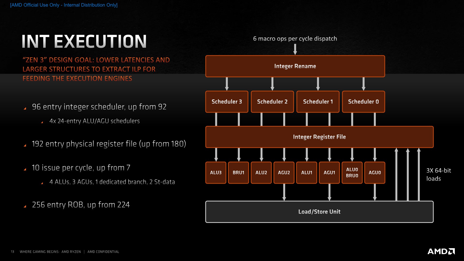
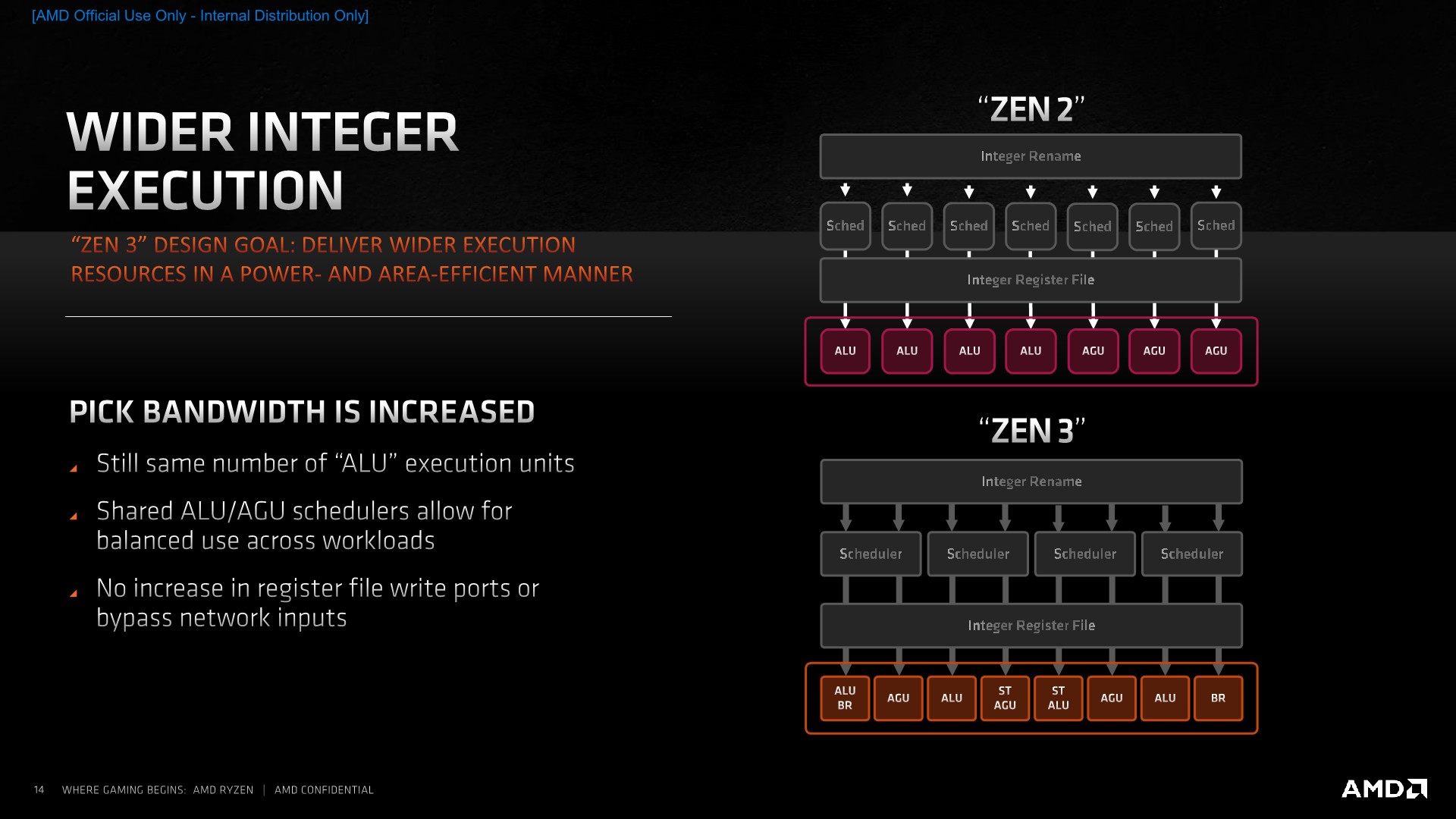
Starting off in more detail on the integer side, the one larger change in the design has been a move from individual schedulers for each of the execution units to a more consolidated design of four schedulers issuing into two execution units each. These new 24-entry schedulers should be more power efficient than having separate smaller schedulers, and the entry capacity also grows slightly from 92 to 96.
The physical register file has seen a slight increase from 180 entries to 192 entries, allowing for a slight increase in the integer OOO-window, with the actual reorder-buffer of the core growing from 224 instructions to 256 instructions, which in the context of competing microarchitectures such as Intel’s 352 ROB in Sunny Cove or Apple giant ROB still seems relatively small.
The overall integer execution unit issue width has grown from 7 to 10. The breakdown here is that while the core still has 4 ALUs, we’ve now seen one of the branch ports separate into its own dedicated unit, whilst the other unit still shares the same port as one of the ALUs, allowing for the unshared ALU to dedicate itself more to actual arithmetic instructions. Not depicted here is an additional store unit, as well as a third load unit, which is what brings us to 10 issue units in total on the integer side.
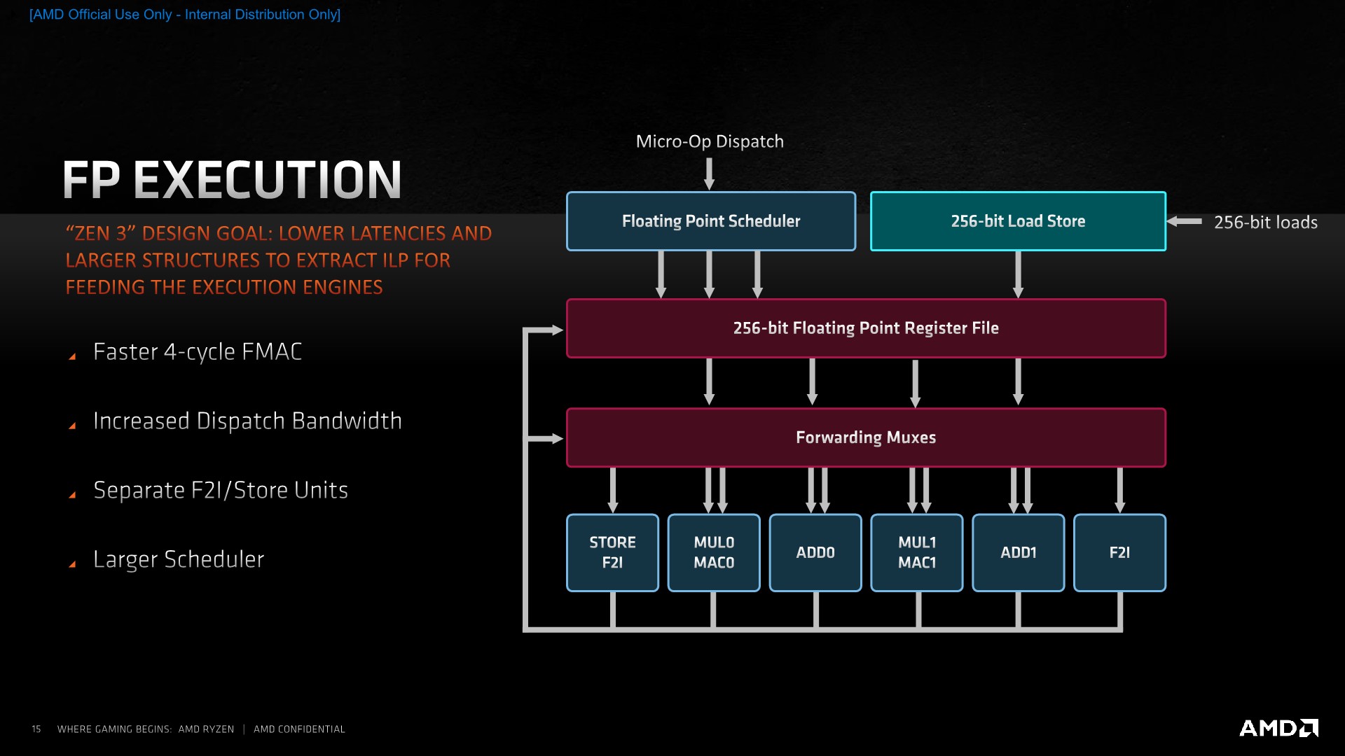
On the floating-point side, the dispatch width has been increased from 4 µOps to 6 µOps. Similar to the integer pipelines, AMD has opted to disaggregate some of the pipelines capabilities, such as moving the floating point store and floating-point-to-integer conversion units into their own dedicated ports and units, so that the main execution pipelines are able to see higher utilisation with actual compute instructions.
One of the bigger improvements in the instruction latencies has been the shaving off of a cycle from 5 to 4 for fused multiply accumulate operations (FMAC). The scheduler on the FP side has also seen an increase in order to handle more in-flight instructions as loads on the integer side are fetching the required operands, although AMD here doesn’t disclose the exact increases.
Section by Andrei Frumusanu
The New Zen 3 Core: Load/Store and a Massive L3 Cache
Although Zen3’s execution units on paper don’t actually provide more computational throughput than Zen2, the rebalancing of the units and the offloading of some of the shared execution capabilities onto dedicated units, such as the new branch port and the F2I ports on the FP side of the core, means that the core does have more actual achieved computational utilisation per cycle. To be able to make sure that memory isn’t a bottleneck, AMD has notably improved the load/store part of the design, introducing some larger changes allowing for some greatly improved memory-side capabilities of the design.
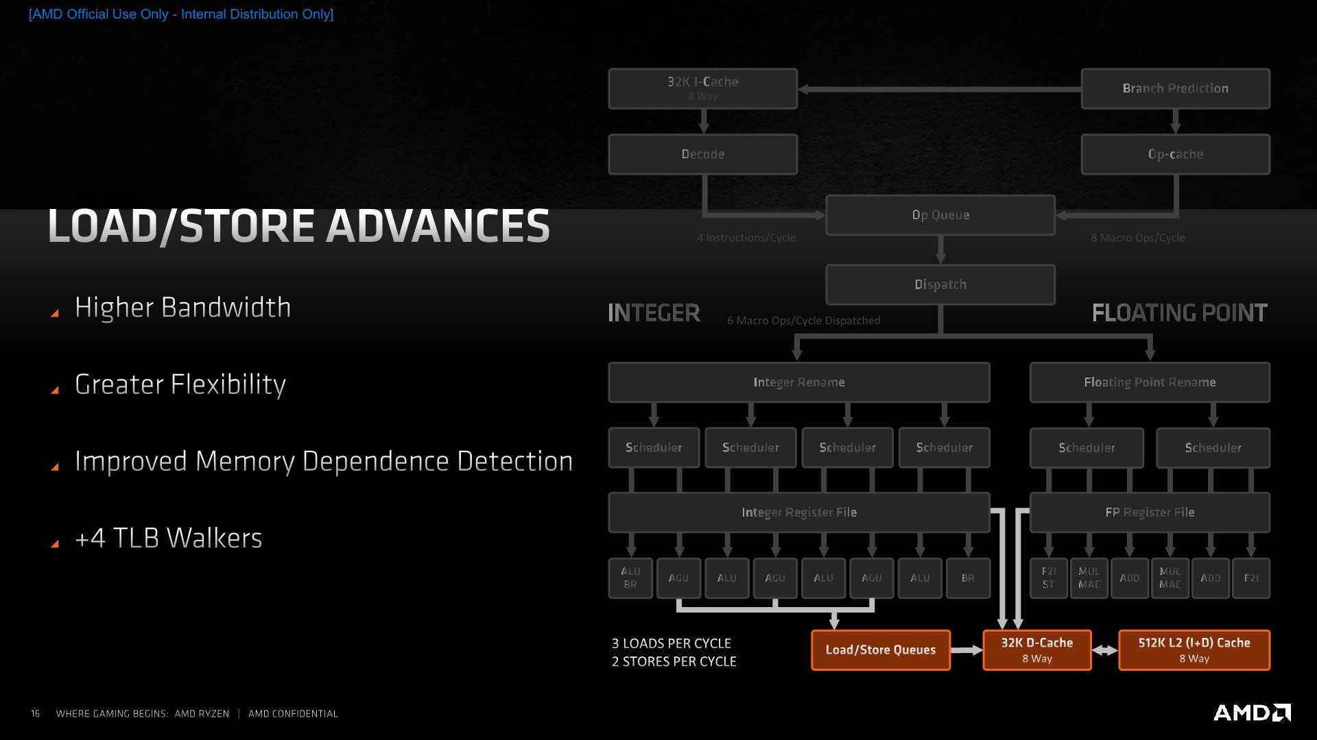
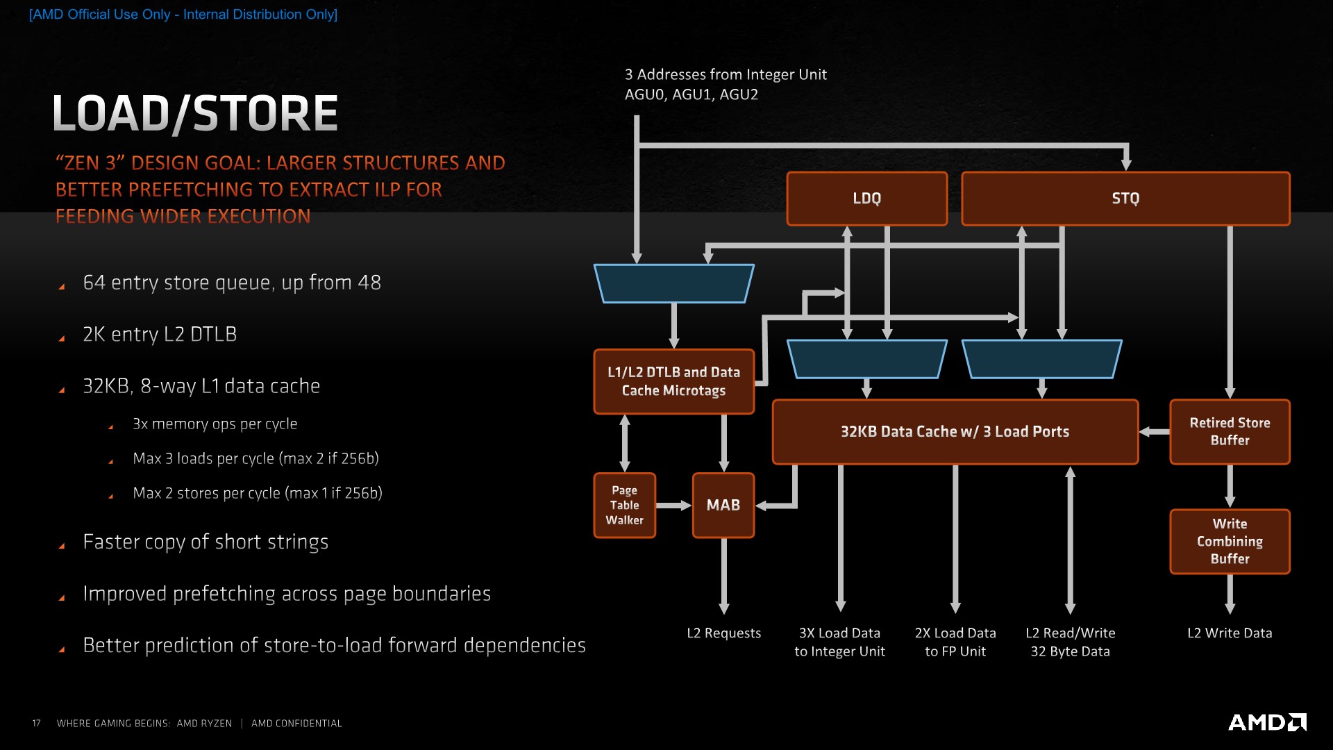
The core now has a higher bandwidth ability thanks to an additional load and store unit, with the total amount of loads and stores per cycle now ending up at 3 and 2. AMD has improved the load to store forwarding to be ablet to better manage the dataflow through the L/S units.
An interesting large upgrade is the inclusion of 4 additional table walkers on top of the 2 existing ones, meaning the Zen3 cores has a total of 6 table walkers. Table-walkers are usually the bottleneck for memory accesses which miss the L2 TLB, and having a greater number of them means that in bursts of memory accesses which miss the TLB, the core can resolve and fetch such parallel access much faster than if it had to rely on one or two table walkers which would have to serially fulfil the page walk requests. In this regard, the new Zen3 microarchitecture should do significantly better in workloads with high memory sparsity, meaning workloads which have a lot of spread out memory accesses across large memory regions.
On the actual load/store units, AMD has increased the depth of the store queue from 48 entries to 64. Oddly enough, the load queue has remained at 44 entries even though the core has 50% higher load capabilities. AMD counts this up to 72 by counting the 28-entry address generation queue.
The L2 DTLB has also remained at 2K entries which is interesting given that this would now only cover 1/4th of the L3 that a single core sees. AMD explains that this is simply a balance between the given performance improvement and the actual implementation complexity – reminding us that particularly in the enterprise market there’s the option to use memory pages larger than your usual 4K size that are the default for consumer systems.
The L1 data cache structure has remained the same in terms of its size, still 32KB and 8-way associative, but now seeing an increase in access concurrency thanks to the 3x loads per cycle that the integer units are able to request. It doesn’t actually change the peak bandwidth of the cache as integer accesses can only be 64b for a total of 192b per cycle when using 3 concurrent loads – the peak bandwidth is still only achieved through 2 256b loads coming from the FP/SIMD pipelines. Stores similarly have been doubled in terms of concurrent operations per cycle, but only on the integer side with 2 64b stores, as the FP/SIMD pipes still peak out at 1 256b store per cycle.
REP MOVS instructions have seen improvements in terms of its efficiencies for shorter buffer sizes. This means that in contrast to past microarchitectures which might have seen better throughput with other copy algorithms, on Zen3 REP MOVS will see optimal performance no matter how big or small the buffer size being copied is.
AMD has also improved their prefetchers, saying that now patterns which cross page boundaries are better detected and predicted. I’ve noted also that the general prefetcher behaviours have dramatically changed, with some patterns, such as adjacent cache lines being pulled into L1, something which is very aggressive, and also more relaxed behaviour, such as some of our custom pattern no longer being as aggressively picked up by then new prefetchers.
AMD says that the store-to-load forwarding prediction is important to the architecture and that there’s some new technology where the core is now more capable of detecting dependencies in the pipeline and forwarding earlier, getting the data to instructions which need them in time.
A Big Fat 32MB L3 Cache
Moving out from the individual cores, we come to the brand-new 32MB L3 cache which is a cornerstone characteristic of the new Zen3 microarchitecture and the new Ryzen 5000 CCD:
The big change here is of a topological nature, as AMD does away with the 4-core CCX which had been previously used as the unified core cluster block for Zen/Zen+/Zen2. Instead of having to divide a chiplet’s total cache capacity into two blocks of 4 and 4 cores, the new unified L3 aggregates the previously laid out SRAM amount into a single large 32MB pool spanning 8 cache slices and servicing 8 cores.
Achieving this larger 32MB L3 cache didn’t come without compromises as latencies have gone up by roughly 7 cycles to 46 cycles total. We asked AMD about the topology of the new cache but they wouldn’t comment on it besides stating that it’s still an address-hash based system across the 8 cache slices, with a flat memory latency across the depth of the cache, from the view of a single core.
One thing that AMD wasn’t able to scale up with the new L3 cache is cache bandwidth – here the new L3 actually features the same interface widths as on Zen2, and total aggregate bandwidth across all the cores peaks out at the same number as on the previous generation. The thing is now, the cache serves double the cores, so it means that the per-core bandwidth has halved this generation. AMD explains is that also scaling up the bandwidth would have incurred further compromises, particularly on the power side of things. In effect this means that the aggregate L3 bandwidth on a CCD, disregarding clock speed improvements, will be half of that of that of a Zen2/Ryzen 3000 CCD with two CCX’s (Essentially two separate L3’s).
The net win of the new structure from greatly improved cache hit rates for application with larger memory pressures, taking advantage of the full 32MB L3, as well as workloads which make use of heavy synchronisation and core-to-core data transfers: Whereas in previous generations two cores in different CCX’s on the same die would have to route traffic through the IOD, this on-die penalty is completely eliminated on Zen3, and all cores within the new CCD have full and low-latency communication to each other through the new L3.
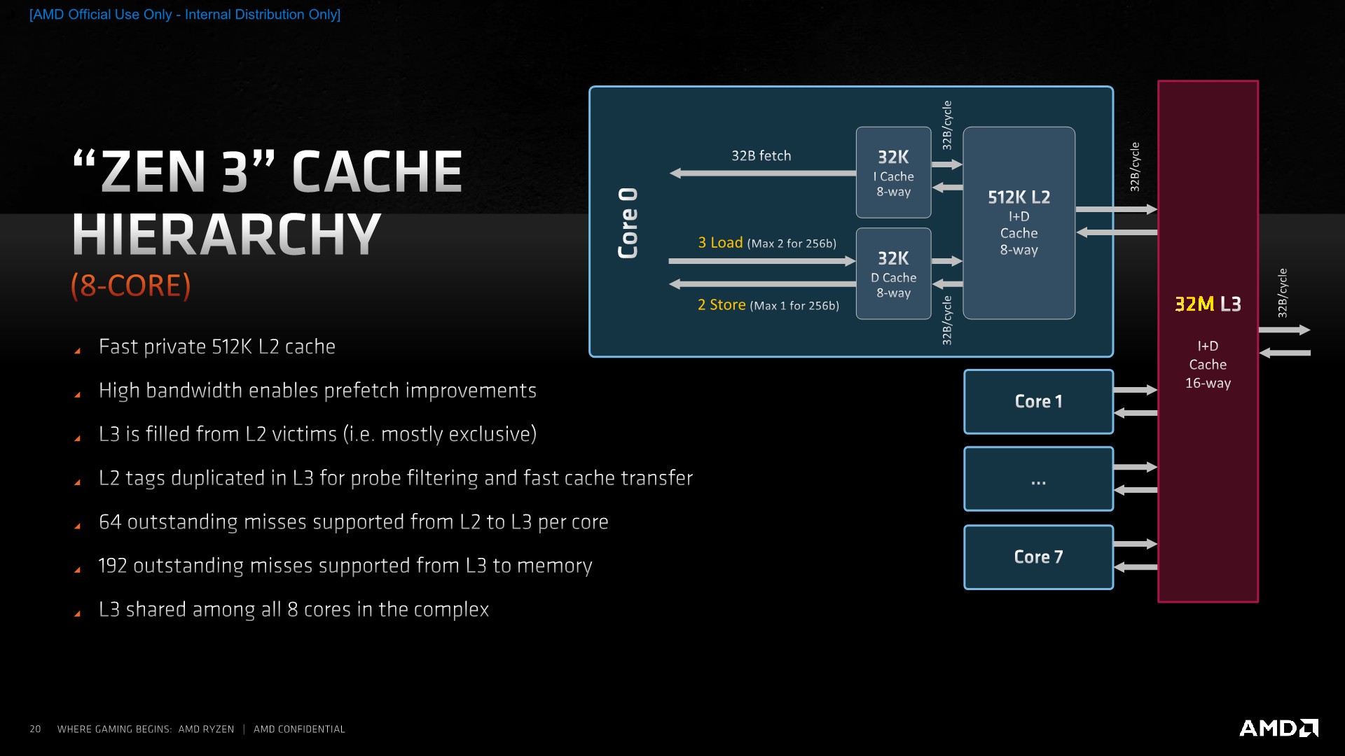
Viewing the whole cache hierarchy on the new Zen3 design, we see a somewhat familiar picture. The L2’s have remained unchanged at 512KB and a 12-cycle access latency, with the memory interfaces from the L1D to through to the L3 coming in at 32B/cycle both in reads and writes.
The L3 continues to maintain shadow tags of the cores’ L2 contents – so if a cache line is requested by one core and resides on another core in the new core complex, the L3 will know from which core to fetch that line back from.
In terms of parallelism, there can be up to 64 outstanding misses from the L2 to the L3, per core. Memory requests from the L3 to DRAM hit a 192 outstanding miss limit – which actually might be a bit low in scenarios where there’s a lot of cores accessing memory at the same time. This is a doubling from the 96 outstanding misses per L3 on Zen2, so the misses per core ratio here at least hasn’t changed.
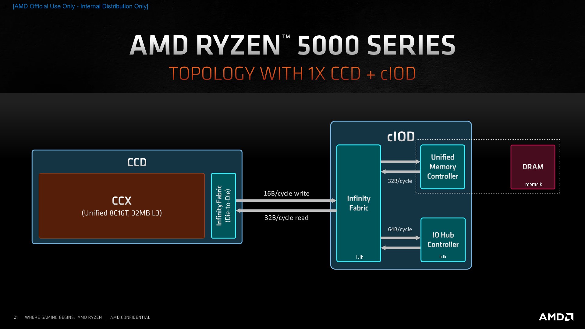
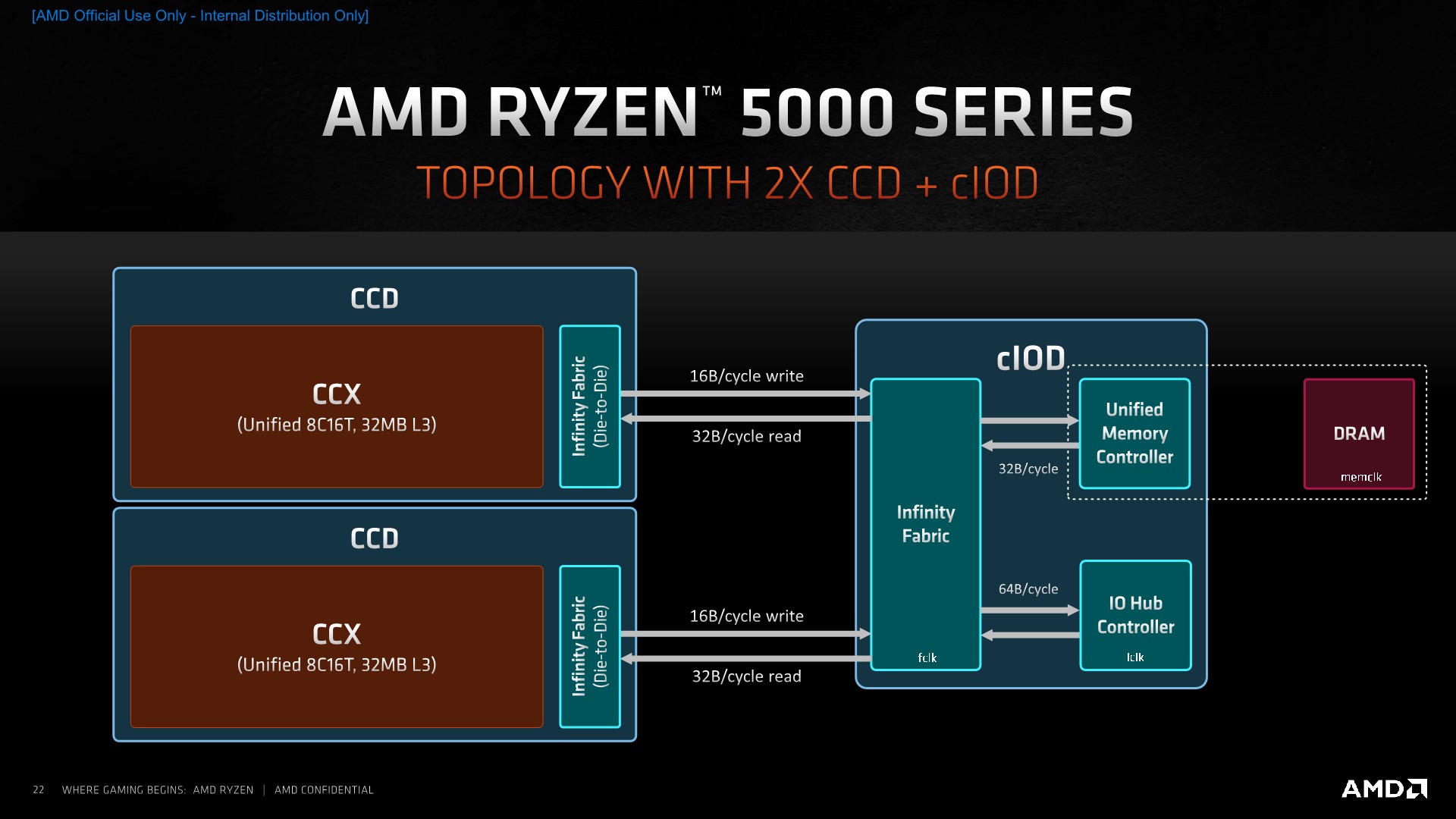
In terms of the packaging topology, because the new Ryzen 5000 series are using the same IOD as the Ryzen 3000 series, we don’t actually see any change in the overall structure of the design. We can either have SKUs with only a single chiplet, such as the new Ryzen 5 5600X or Ryzen 7 5800X, or deploy two chiplets, such as the Ryzen 9 5900X or Ryzen 9 5950X.
The bandwidth between the CCD and the IOD remains the same between generations, with 16B/cycle writes from the CCD to the IOD, and 32B/cycle reads in the opposite direction. Infinity fabric speed is the determining factor for the resulting bandwidth here, which AMD still recommends to be coupled 1:1 with DRAM frequency for the best memory latency, at least until around DDR4-3600, and slightly above for overclockers.
While we’ll be covering the end-performance and actual IPC improvements of Zen3 in the following pages, the first impressions based on AMD’s microarchitectural disclosures are that the new design is indeed a larger-than-average effort in the company’s CPU roadmap.
AMD calls Zen3 a ground-up redesign or even a clean-sheet design. Whilst that seems a quite lofty description of the new microarchitecture, it’s true that at least the architects have touched a lot of aspects of the design, even if at the end a lot of the structures and actual overall width of the core, especially on the front-end, hasn’t actually changed all that much from Zen2.
My view of what Zen3 is, is that it’s a rebuild of the previous generation, with AMD taking lessons from the past implementation and improving and refining the overall broader design. When asked about future potential for widening the core, similarly to some of the current competing microarchitectures out there, AMD’s Mike Clarke admitted that at some point they will have to do that to make sure they don’t fall behind in performance, and that they are already working on another future clean-sheet redesign. For the time being, Zen3 was the right choice in terms balancing out performance, efficiency, time-to-market, as well as considering that this generation actually didn’t have a large process node uplift (Which by the way, will be a rarer and increasingly unreliable vector for improving performance in the future).
I do hope that these designs come in a timely fashion with impressive changes, as the competition from the Arm side is definitely heating up, with designs such as the Cortex-X1 or the Neoverse-V1 appearing to be more than a match for lower-clocked Zen3 designs (such as in the server/enterprise space). On the consumer side of things, AMD appears to be currently unrivalled, although we’ll be keeping an eye open for the upcoming Apple silicon.
Section by Andrei Frumusanu
Core-to-Core Latency
As the core count of modern CPUs is growing, we are reaching a time when the time to access each core from a different core is no longer a constant. Even before the advent of heterogeneous SoC designs, processors built on large rings or meshes can have different latencies to access the nearest core compared to the furthest core. This rings true especially in multi-socket server environments.
But modern CPUs, even desktop and consumer CPUs, can have variable access latency to get to another core. For example, in the first generation Threadripper CPUs, we had four chips on the package, each with 8 threads, and each with a different core-to-core latency depending on if it was on-die or off-die. This gets more complex with products like Lakefield, which has two different communication buses depending on which core is talking to which.
If you are a regular reader of AnandTech’s CPU reviews, you will recognize our Core-to-Core latency test. It’s a great way to show exactly how groups of cores are laid out on the silicon. This is a custom in-house test, and we know there are competing tests out there, but we feel ours is the most accurate to how quick an access between two cores can happen.
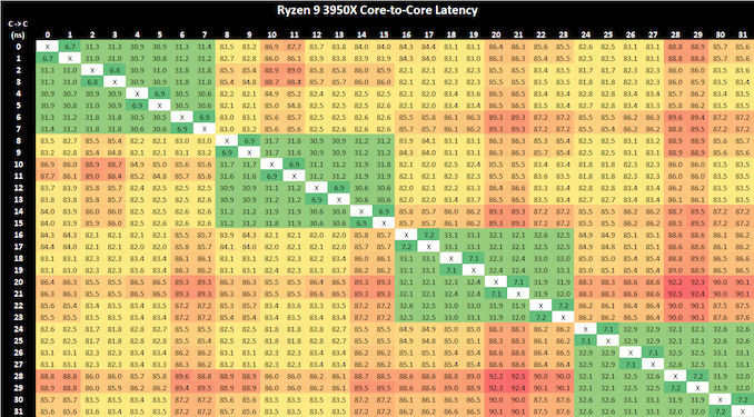
We had noted some differences in the core-to-core latency behaviour of various Zen2 CPUs depending on which motherboard and which AGESA version was tested at the time. For example, in this current version we’re seeing inter-core latencies within the L3 caches of the CCX’s falling in at around 30-31ns, however in the past we had measured on the same CPU figures in the 17ns range. We had measured a similar figure on our Zen2 Renoir tests, so it’s all the more odd to now get a 31ns figure on the 3950X while on a different motherboard. We had reached out to AMD about this odd discrepancy but never really got a proper response as to what exactly is happening here – it’s after all the same CPU and even the same test binary, just differing motherboard platforms and AGESA versions.
Nevertheless, in the result we can clearly see the low-latencies of the four CCXs, with inter-core latencies between CPUs of differing CCXs suffering to a greater degree in the 82ns range, which remains one of the key disadvantages of AMD’s core complex and chiplet architecture.
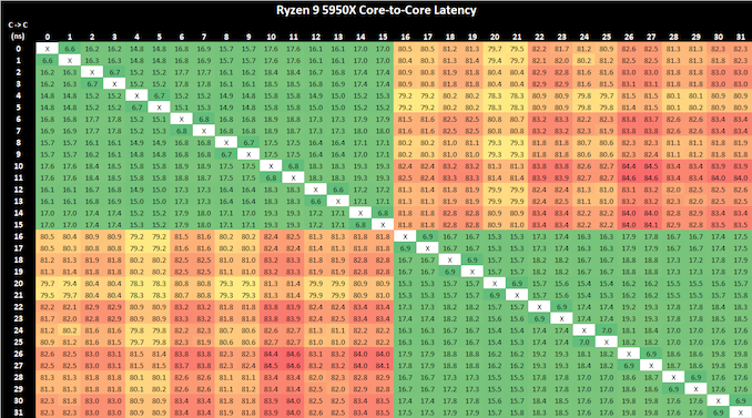
On the new Zen3-based Ryzen 9 5950X, what immediately is obvious is that instead of four low-latency CPU clusters, there are now only two of them. This corresponds to AMD’s switch from four CCX’s for their 16-core predecessor, to only two such units on the new part, with the new CCX basically being the whole CCD this time around.
Inter-core latencies within the L3 lie in at 15-19ns, depending on the core pair. One aspect affecting the figures here are also the boost frequencies of that the core pairs can reach as we’re not fixing the chip to a set frequency. This is a large improvement in terms of latency over the 3950X, but given that in some firmware combinations, as well as on AMD’s Renoir mobile chip this is the expected normal latency behaviour, it doesn’t look that the new Zen3 part improves much in that regard, other than obviously of course enabling this latency over a greater pool of 8 cores within the CCD.
Inter-core latencies between cores in different CCDs still incurs a larger latency penalty of 79-80ns, which is somewhat to be expected as the new Ryzen 5000 parts don’t change the IOD design compared to the predecessor, and traffic would still have to go through the infinity fabric on it.
For workloads which are synchronisation heavy and are multi-threaded up to 8 primary threads, this is a great win for the new Zen3 CCD and L3 design. AMD’s new L3 complex in fact now offers better inter-core latencies and a flatter topology than Intel’s ring-based consumer designs, with SKUs such as the 10900K varying between 16.5-23ns inter-core latency. AMD still has a way to go to reduce inter-CCD latency, but maybe that something to address in the next generation design.
Cache and Memory Latency
As Zen3 makes some big changes in the memory cache hierarchy department, we’re also expecting this to materialise in quite different behaviour in our cache and memory latency tests. On paper, the L1D and L2 caches on Zen3 shouldn’t see any differences when compared to Zen2 as both share the same size and cycle latencies – however we did point out in our microarchitecture deep dive that AMD did make some changes to the behaviour here due to the prefetchers as well as cache replacement policy.
On the L3 side, we expect a large shift of the latency curve into deeper memory regions given that a single core now has access to the full 32MB, double that of the previous generation. Deeper into DRAM, AMD actually hasn’t talked much at all about how memory latency would be affected by the new microarchitecture – we don’t expect large changes here due to the fact that the new chips are reusing the same I/O die with the same memory controllers and infinity fabric. Any latency effects here should be solely due to the microarchitectural changes made on the actual CPUs and the core-complex die.
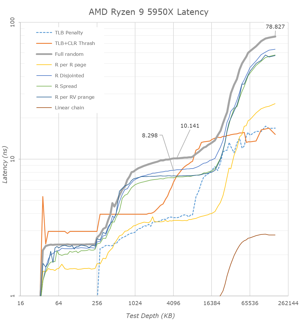
Starting off in the L1D region of the new Zen3 5950X top CPU, we’re seeing access latencies of 0.792ns which corresponds to a 4-cycle access at exactly 5050MHz, which is the maximum frequency at which this new part boosts to in single-threaded workloads.
Entering the L2 region, we however are already starting to see some very different microarchitectural behaviour on the part of the latency tests as they look nothing like we’ve seen on Zen2 and prior generations.
Starting off with the most basic access pattern, a simple linear chain within the address space, we’re seeing access latencies improve from an average of 5.33 cycles on Zen2 to +-4.25 cycles on Zen3, meaning that this generation’s adjacent-line prefetchers are much more aggressive in pulling data into the L1D. This is actually now even more aggressive than Intel’s cores, which have an average access latency of 5.11 cycles for the same pattern within their L2 region.
Besides the simple linear chain, we also see very different behaviour in a lot of the other patterns, some of our other more abstract patterns aren’t getting prefetched as aggressively as on Zen2, more on that later. More interestingly is the behaviour of the full random access and the TLB+CLR trash pattern which are now completely different: The full random curve is now a lot more abrupt on the L1 to L2 boundary, and we’re seeing the TLB+CLR having an odd (reproducible) spike here as well. The TLB+CLR pattern goes through random pages always hitting only a single, but every time different cache line within each page, forcing a TLB read (or miss) as well as a cache line replacement.
The fact that this test now behaves completely different throughout the L2 to L3 and DRAM compared to Zen2 means that AMD is now employing a very different cache line replacement policy on Zen3. The test’s curve in the L3 no longer actually matching the cache’s size means that AMD is now optimising the replacement policy to reorder/move around cache lines within the sets to reduce unneeded replacements within the cache hierarchies. In this case it’s a very interesting behaviour that we hadn’t seen to this degree in any microarchitecture and basically breaks our TLB+CLR test which we previously relied on for estimating the physical structural latencies of the designs.
It’s this new cache replacement policy which I think is cause for the more smoothed out curves when transitioning between the L2 and L3 caches as well as from the L3 to DRAM – the latter behaviour which now looks closer to what Intel and some other competing microarchitectures have recently exhibited.
Within the L3, things are a bit difficult to measure as there’s now several different effects at play. The prefetchers on Zen3 don’t seem to be as aggressive on some of our patterns which is why the latency here has gone up more a little bit more of a notable amount – we can’t really use them for apples-to-apples comparisons to Zen2 because they’re no longer doing the same thing. Our CLR+TLB test also not working as intended means that we’ll have to resort to full random figures; the new Zen3 cache at 4MB depth here measured in at 10.127ns on the 5950X, compared to 9.237ns on the 3950X. Translating this into cycles corresponds to a regression from 42.9 cycles to 51.1 cycles on average, or basically +8 cycles. AMD’s official figures here are 39 cycles and 46 cycles for Zen2 and Zen3, a +7-cycle regression – in line with what we measure, accounting for TLB effects.
Latencies past 8MB still go up even though the L3 is 32MB deep, and that’s simply because it exceeds the L2 TLB capacity of 2K pages with a 4K page size.
In the DRAM region, we’re measuring 78.8ns on the 5950X versus 86.0ns on the 3950X. Converting this into cycles actually ends up with an identical 398 cycles for both chips at 160MB full random-access depth. We have to note that because of that change in the cache line replacement policy that latencies appear to be better for the new Zen3 chip at test depths between 32-128MB, but that’s just a measurement side-effect and does not seem to be an actual representation of the physical and structural latency of the new chip. You’d have to test deeper DRAM regions to get accurate figures – all of which makes sense given that the new Ryzen 5000 chips are using the same I/O die and memory controllers, and we’re testing identical memory at the same 3200MHz speed.
Overall, although Zen3 doesn’t change dramatically in its cache structure beyond the doubled up and slightly slower L3, the actual cache behaviour between microarchitecture generations has changed quite a lot for AMD. The new Zen3 design seems to make much smarter use of prefetching as well as cache line handling – some of whose performance effects could easily overshadow just the L3 increase. We inquired AMD’s Mike Clarke about some of these new mechanisms, but the company wouldn’t comment on some of the new technologies that they would rather keep closer to their chest for the time being.
Frequency Ramping
Both AMD and Intel over the past few years have introduced features to their processors that speed up the time from when a CPU moves from idle into a high powered state. The effect of this means that users can get peak performance quicker, but the biggest knock-on effect for this is with battery life in mobile devices, especially if a system can turbo up quick and turbo down quick, ensuring that it stays in the lowest and most efficient power state for as long as possible.
Intel’s technology is called SpeedShift, although SpeedShift was not enabled until Skylake.
One of the issues though with this technology is that sometimes the adjustments in frequency can be so fast, software cannot detect them. If the frequency is changing on the order of microseconds, but your software is only probing frequency in milliseconds (or seconds), then quick changes will be missed. Not only that, as an observer probing the frequency, you could be affecting the actual turbo performance. When the CPU is changing frequency, it essentially has to pause all compute while it aligns the frequency rate of the whole core.
We wrote an extensive review analysis piece on this, called ‘Reaching for Turbo: Aligning Perception with AMD’s Frequency Metrics’, due to an issue where users were not observing the peak turbo speeds for AMD’s processors.
We got around the issue by making the frequency probing the workload causing the turbo. The software is able to detect frequency adjustments on a microsecond scale, so we can see how well a system can get to those boost frequencies. Our Frequency Ramp tool has already been in use in a number of reviews.
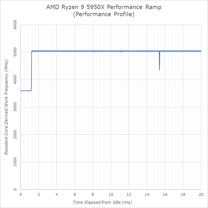
On the performance profile, the new 5950X looks to behave identical to the Ryzen 3000 series, ramping up to maximum frequency in 1.2ms. On the balanced profile, this is at 18ms to avoid needlessly upping the frequency from idle during sporadic background tasks.
Idle frequency on the new CPU lands in at 3597MHz and the Zen3 CPU here will boost up to 5050MHz on single-threaded workloads. In our test tool it actually reads out fluctuations between 5025 and 5050MHz, however that just seems to be an aliasing issue due to the timer resolution being 100ns and us measuring 20µs workload chunks. The real frequency as per base-clock and multiplier looks to be 5048.82MHz on this particular motherboard.
New and Improved Instructions
When it comes to instruction improvements, moving to a brand new ground-up core enables a lot more flexibility in how instructions are processed compared to just a core update. Aside from adding new security functionality, being able to rearchitect the decoder/micro-op cache, the execution units, and the number of execution units allows for a variety of new features and hopefully faster throughput.
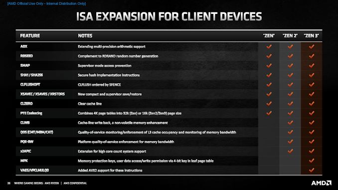
As part of the microarchitecture deep-dive disclosures from AMD, we naturally get AMD’s messaging on the improvements in this area – we were told of the highlights, such as the improved FMAC and new AVX2/AVX256 expansions. There’s also Control-Flow Enforcement Technology (CET) which enables a shadow stack to protect against ret/ROP attacks. However after getting our hands on the chip, there’s a trove of improvements to dive through.
Let’s cover AMD’s own highlights first.
The top cover item is the improved Fused Multiply-Accumulate (FMA), which is a frequently used operation in a number of high-performance compute workloads as well as machine learning, neural networks, scientific compute and enterprise workloads.
In Zen 2, a single FMA took 5 cycles with a throughput of 2/clock.
In Zen 3, a single FMA takes 4 cycles with a throughput of 2/clock.
This means that AMD’s FMAs are now on parity with Intel, however this update is going to be most used in AMD’s EPYC processors. As we scale up this improvement to the 64 cores of the current generation EPYC Rome, any compute-limited workload on Rome should be freed in Naples. Combine that with the larger L3 cache and improved load/store, some workloads should expect some good speed ups.
The other main update is with cryptography and cyphers. In Zen 2, vector-based AES and PCLMULQDQ operations were limited to AVX / 128-bit execution, whereas in Zen 3 they are upgraded to AVX2 / 256-bit execution.
This means that VAES has a latency of 4 cycles with a throughput of 2/clock.
This means that VPCLMULQDQ has a latency of 4 cycles, with a throughput of 0.5/clock.
AMD also mentioned to a certain extent that it has increased its ability to process repeated MOV instructions on short strings – what used to not be so good for short copies is now good for both small and large copies. We detected that the new core performs better REP MOV instruction elimination at the decode stage, leveraging the micro-op cache better.
Now here’s the stuff that AMD didn’t talk about.
Integer
Sticking with instruction elimination, a lot of instructions and zeroing idioms that Zen 2 used to decode but then skip execution are now detected and eliminated at the decode stage.
- NOP (90h) up to 5x 66h
- LNOP3/4/5 (Looped NOP)
- (V)MOVAPS/MOVAPD/MOVUPS/MOVUPD vec1, vec1 : Move (Un)Aligned Packed FP32/FP64
- VANDNPS/VANDNPD vec1, vec1, vec1 : Vector bitwise logical AND NOT Packed FP32/FP64
- VXORPS/VXORPD vec1, vec1, vec1 : Vector bitwise logical XOR Packed FP32/FP64
- VPANDN/VPXOR vec1, vec1, vec1 : Vector bitwise logical (AND NOT)/XOR
- VPCMPGTB/W/D/Q vec1, vec1, vec1 : Vector compare packed integers greater than
- VPSUBB/W/D/Q vec1, vec1, vec1 : Vector subtract packed integers
- VZEROUPPER : Zero upper bits of YMM
- CLC : Clear Carry Flag
As for direct performance adjustments, we detected the following:
| Zen3 Updates (1) Integer Instructions |
|||
| AnandTech | Instruction | Zen2 | Zen 3 |
| XCHG | Exchange Register/Memory with Register |
17 cycle latency | 7 cycle latency |
| LOCK (ALU) | Assert LOCK# Signal | 17 cycle latency | 7 cycle latency |
| ALU r16/r32/r64 imm | ALU on constant | 2.4 per cycle | 4 per cycle |
| SHLD/SHRD | FP64 Shift Left/Right | 4 cycle latency 0.33 per cycle |
2 cycle latency 0.66 per cycle |
| LEA [r+r*i] | Load Effective Address | 2 cycle latency 2 per cycle |
1 cycle latency 4 per cycle |
| IDIV r8 | Signed Integer Division | 16 cycle latency 1/16 per cycle |
10 cycle latency 1/10 per cycle |
| DIV r8 | Unsigned Integer Division | 17 cycle latency 1/17 per cycle |
|
| IDIV r16 | Signed Integer Division | 21 cycle latency 1/21 per cycle |
12 cycle latency 1/12 per cycle |
| DIV r16 | Unsigned Integer Division | 22 cycle latency 1/22 per cycle |
|
| IDIV r32 | Signed Integer Division | 29 cycle latency 1/29 per cycle |
14 cycle latency 1/14 per cycle |
| DIV r32 | Unsigned Integer Division | 30 cycle latency 1/30 per cycle |
|
| IDIV r64 | Signed Integer Division | 45 cycle latency 1/45 per cycle |
19 cycle latency 1/19 per cycle |
| DIV r64 | Unsigned Integer Division | 46 cycle latency 1/46 cycle latency |
20 cycle latency 1/20 per cycle |
| Zen3 Updates (2) Integer Instructions |
|||
| AnandTech | Instruction | Zen2 | Zen 3 |
| LAHF | Load Status Flags into AH Register |
2 cycle latency 0.5 per cycle |
1 cycle latency 1 per cycle |
| PUSH reg | Push Register Onto Stack | 1 per cycle | 2 per cycle |
| POP reg | Pop Value from Stack Into Register |
2 per cycle | 3 per cycle |
| POPCNT | Count Bits | 3 per cycle | 4 per cycle |
| LZCNT | Count Leading Zero Bits | 3 per cycle | 4 per cycle |
| ANDN | Logical AND | 3 per cycle | 4 per cycle |
| PREFETCH* | Prefetch | 2 per cycle | 3 per cycle |
| PDEP/PEXT | Parallel Bits Deposit/Extreact |
300 cycle latency 250 cycles per 1 |
3 cycle latency 1 per clock |
It’s worth highlighting those last two commands. Software that helps the prefetchers, due to how AMD has arranged the branch predictors, can now process three prefetch commands per cycle. The other element is the introduction of a hardware accelerator with parallel bits: latency is reduced 99% and throughput is up 250x. If anyone asks why we ever need extra transistors for modern CPUs, it’s for things like this.
There are also some regressions
| Zen3 Updates (3) Slower Instructions |
|||
| AnandTech | Instruction | Zen2 | Zen 3 |
| CMPXCHG8B | Compare and Exchange 8 Byte/64-bit |
9 cycle latency 0.167 per cycle |
11 cycle latency 0.167 per cycle |
| BEXTR | Bit Field Extract | 3 per cycle | 2 per cycle |
| BZHI | Zero High Bit with Position | 3 per cycle | 2 per cycle |
| RORX | Rorate Right Logical Without Flags |
3 per cycle | 2 per cycle |
| SHLX / SHRX | Shift Left/Right Without Flags |
3 per cycle | 2 per cycle |
As always, there are trade offs.
x87
For anyone using older mathematics software, it might be riddled with a lot of x87 code. x87 was originally meant to be an extension of x86 for floating point operations, but based on other improvements to the instruction set, x87 is somewhat deprecated, and we often see regressed performance generation on generation.
But not on Zen 3. Among the regressions, we’re also seeing some improvements. Some.
| Zen3 Updates (4) x87 Instructions |
|||
| AnandTech | Instruction | Zen2 | Zen 3 |
| FXCH | Exchange Registers | 2 per cycle | 4 per cycle |
| FADD | Floating Point Add | 5 cycle latency 1 per cycle |
6.5 cycle latency 2 per cycle |
| FMUL | Floating Point Multiply | 5 cycle latency 1 per cycle |
6.5 cycle latency 2 per cycle |
| FDIV32 | Floating Point Division | 10 cycle latency 0.285 per cycle |
10.5 cycle latency 0.800 per cycle |
| FDIV64 | 13 cycle latency 0.200 per cycle |
13.5 cycle latency 0.235 per cycle |
|
| FDIV80 | 15 cycle latency 0.167 per cycle |
15.5 cycle latency 0.200 per cycle |
|
| FSQRT32 | Floating Point Square Root |
14 cycle latency 0.181 per cycle |
14.5 cycle latency 0.200 per cycle |
| FSQRT64 | 20 cycle latency 0.111 per cycle |
20.5 cycle latency 0.105 per cycle |
|
| FSQRT80 | 22 cycle latency 0.105 per cycle |
22.5 cycle latency 0.091 per cycle |
|
| FCOS 0.739079 |
cos X = X | 117 cycle latency 0.27 per cycle |
149 cycle latency 0.28 per cycle |
The FADD and FMUL improvements mean the most here, but as stated, using x87 is not recommended. So why is it even mentioned here? The answer lies in older software. Software stacks built upon decades old Fortran still use these instructions, and more often than not in high performance math codes. Increasing throughput for the FADD/FMUL should provide a good speed up there.
Vector Integers
All of the vector integer improvements fall into two main categories. Aside from latency improvements, some of these improvements are execution port specific – due to the way the execution ports have changed this time around, throughput has improved for large numbers of instructions.
| Zen3 Updates (5) Port Vector Integer Instructions |
||||
| AnandTech | Instruction | Vector | Zen2 | Zen 3 |
| FP013 -> FP0123 | ALU, BLENDI, PCMP, MIN/MAX | MMX, SSE, AVX, AVX2 | 3 per cycle | 4 per cycle |
| FP2 Non-Variable Shift | PSHIFT | MMX, SSE AVX, AVX2 |
1 per clock | 2 per clock |
| FP1 | VPSRLVD/Q VPSLLVD/Q |
AVX2 | 3 cycle latency 0.5 per clock |
1 cycle latency 2 per clock |
| DWORD FP0 | MUL/SAD | MMX, SSE, AVX, AVX2 | 3 cycle latency 1 per clock |
3 cycle latency 2 per cycle |
| DWORD FP0 | PMULLD | SSE, AVX, AVX2 | 4 cycle latency 0.25 per clock |
3 cycle latency 2 per clock |
| WORD FP0 int MUL | PMULHW, PMULHUW, PMULLW | MMX, SSE, AVX, AVX2 | 3 cycle latency 1 per clock |
3 cycle latency 0.6 per clock |
| FP0 int | PMADD, PMADDUBSW | MMX, SSE, AVX, AVX2 | 4 cycle latency 1 per clock |
3 cycle latency 2 per clock |
| FP1 insts | (V)PERMILPS/D, PHMINPOSUW EXTRQ, INSERTQ |
SSE4a | 3 cycle latency 0.25 per clock |
3 cycle latency 2 per clock |
There are a few others not FP specific.
| Zen3 Updates (6) Vector Integer Instructions |
||||
| AnandTech | Instruction | Zen2 | Zen 3 | |
| VPBLENDVB | xmm/ymm | Variable Blend Packed Bytes | 1 cycle latency 1 per cycle |
1 cycle latency 2 per cycle |
| VPBROADCAST B/W/D/SS |
ymm<-xmm | Load and Broadcast | 4 cycle latency 1 per cycle |
2 cycle latency 1 per cycle |
| VPBROADCAST Q/SD |
ymm<-xmm | Load and Broadcast | 1 cycle latency 1 per cycle |
2 cycle latency 1 per cycle |
| VINSERTI128 VINSERTF128 |
ymm<-xmm | Insert Packed Values | 1 cycle latency 1 per cycle |
2 cycle latency 1 per cycle |
| SHA1RNDS4 | Four Rounds of SHA1 | 6 cycle latency 0.25 per cycle |
6 cycle latency 0.5 per cycle |
|
| SHA1NEXTE | Calculate SHA1 State | 1 cycle latency 1 per cycle |
1 cycle latency 2 per cycle |
|
| SHA256RNDS2 | Four Rounds of SHA256 | 4 cycle latency 0.5 per cycle |
4 cycle latency 1 per cycle |
|
These last three are important for SHA cryptography. AMD, unlike Intel, does accelerated SHA so being able to reduce multiple instructions to a single instruction to help increase throughput and utilization should push them even further ahead. Rather than going for hardware accelerated SHA256, Intel instead prefers to use its AVX-512 unit, which unfortunately is a lot more power hungry and less efficient.
Vector Floats
We’ve already covered the improvements to the FMA latency, but there are also other improvements.
| Zen3 Updates (7) Vector Float Instructions |
||||
| AnandTech | Instruction | Zen2 | Zen 3 | |
| DIVSS/PS | xmm, ymm | Divide FP32 Scalar/Packed |
10 cycle latency 0.286 per cycle |
10.5 cycle latency 0.444 per cycle |
| DIVSD/PD | xmm, ymm | Divide FP64 Scalar/Packed |
13 cycle latency 0.200 per cycle |
13.5 cycle latency 0.235 per cycle |
| SQRTSS/PS | xmm, ymm | Square Root FP32 Scalar/Packed |
14 cycle latency 0.181 per cycle |
14.5 cycle latency 0.273 per cycle |
| SQRTSD/PD | xmm, ymm | Square Root FP64 Scalar/Packed |
20 cycle latency 0.111 per cycle |
20.5 cycle latency 0.118 per cycle |
| RCPSS/PS | xmm, ymm | Reciprocal FP32 Scalar/Packed |
5 cycle latency 2 per cycle |
3 cycle latency 2 per cycle |
| RSQRTSS/PS | xmm, ymm | Reciprocal FP32 SQRT Scalar/Pack |
5 cycle latency 2 per cycle |
3 cycle latency 2 per cycle |
| VCVT* | xmm<-xmm | Convert | 3 cycle latency 1 per cycle |
3 cycle latency 2 per cycle |
| VCVT* | xmm<-ymm ymm<-xmm |
Convert | 4 cycle latency 1 per cycle |
4 cycle latency 2 per cycle |
| ROUND* | xmm, ymm | Round FP32/FP64 Scalar/Packed |
3 cycle latency 1 per cycle |
3 cycle latency 2 per cycle |
| GATHER | 4x32 | Gather | 19 cycle latency 0.111 per cycle |
15 cycle latency 0.250 per cycle |
| GATHER | 8x32 | Gather | 23 cycle latency 0.063 per cycle |
19 cycle latency 0.111 per cycle |
| GATHER | 4x64 | Gather | 18 cycle latency 0.167 per cycle |
13 cycle latency 0.333 per cycle |
| GATHER | 8x64 | Gather | 19 cycle latency 0.111 per cycle |
15 cycle latency 0.250 per cycle |
Along with these, store-to-load latencies have increased by a clock. AMD is promoting that it has improved store-to-load bandwidth with the new core, but that comes at additional latency.
Compared to some of the recent CPU launches, this is a lot of changes!
Frequency: Going Above 5.0 GHz
One of the major highlights that AMD is promoting with the new Zen 3 core and Ryzen 5000 processors how the company has kept the same power and yet delivered both more frequency, more performance per MHz, and ultimately more performance, despite using the same TSMC N7 manufacturing process node. The updated efficiency of the core, assuming the design can scale in frequency and voltage, can naturally lead to those higher frequency numbers. One of AMD’s humps in competing against Intel of late has been, despite any IPC difference, the higher frequency of Intel’s 14nm process. With Zen 3, we are seeing AMD drive those higher numbers – and some numbers higher than on the box.
When AMD announced the top 16-core processor, the Ryzen 9 5950X, it gave a base frequency of 3400 MHz and a turbo frequency of 4900 MHz. This turbo value was so close to the ‘magic’ number of 5000 MHz, and would yield an additional angle for AMD in its marketing strategy and promotional toolkit. Ultimately scoring a 5000 MHz version comes down to binning – AMD would have detailed analysis of the chiplets it makes at TSMC, and it would see how many chiplets could hit this mark. The question then becomes if there would be enough to satisfy demand, or if those chiplets were better suited in higher efficiency future EPYC products where the margins are higher.
We have seen what happens when you launch a processor that can’t be built in the numbers required: Intel’s Core i9-10900K, at 5.3 GHz turbo, was a super high frequency but couldn’t be built enough to meet demand, and Intel launched the Core i9-10850K – an identical chip except now down to 5.1 GHz, which was an easier target to meet.
If you’ve read through this far in the review, you have already seen that we’re here quoting going above 5.0 GHz for the Ryzen 9 5950X. Despite having an official single core turbo of 4.9 GHz, the processor has an internal metric of ‘peak’ frequency assuming there is sufficient thermal and power headroom of 5025 MHz. This in effect should be its official turbo value. In combination with the default precision boost behavior, we saw a very regular and sustained 5050 MHz.
We quizzed AMD on this. We were told that the 4.9 GHz value for single core turbo should cover all situations, based on BIOS version, motherboard used, and the quality of the silicon inside. The company is happy to let the base precision boost algorithms (or what eXtreme Frequency Range/XFR was rolled into) enable something higher than 4.9 GHz if it can, and they confirmed that with a standard high-end AM4 built and this processor, 5025/5050 MHz should be easily achievable with a large proportion of 5950X retail hardware.
So Why Does AMD Not Promote 5.0 GHz?
From the standpoint of ‘I’ve dealt with press relations from these companies for over 10 years’, I suspect the real answer for AMD not promoting 5.0 GHz is more about sculpting the holistic view of Zen 3 and Ryzen 5000.
If the company were to promote/place the Ryzen 9 5950X as AMD’s second ever processor to go above 5.0 GHz (the first was the FX-9590 back in 2013), or reaching 5.0 GHz on 7nm, then this achievement would necessarily overshadow all of AMD’s other achievements on Zen 3. Rather than pointing to the new core, the increased IPC, or the efficiency of the new processor, everyone would be pointing to the 5.0 GHz frequency instead. Achieving that value and promoting it as such effectively masks the ability for AMD (and the press) to be able to discuss some of the other major wins – that 5.0 GHz win would come off as a poisoned chalice. Not only this, but it might spur users to purchase them at a higher rate; you might consider this a win from both a revenue and gross margins perspective, but it does tie in to AMD’s ability to produce the chiplets at this frequency or if they want to use them for other higher margin products.
Of course, some of this is vanity. AMD would rather speak to its engineering expertise and successes, its teams of engineers, and dive into the specific performance wins, especially for a product where the claims about absolute performance leadership are in-of-themselves a strong statement. Users might conflate the fact that AMD reaching 5.0 GHz was the only reason for performance leadership, and that’s ultimately not the narrative that AMD wants to cultivate.
It also leaves the door open to a future product that will certainly say 5.0 GHz on the box. When AMD has extracted the marketing performance of its increased IPC and efficiency, it can open that window and reap another focused review cycle.
In short: effective marketing is a skill, especially when there are multiple angles that can be leveraged for promotional tools. Identifying how you layer those communications could drastically affect, multiply, or amplify product perception. In what order you execute those multiples and amplifications can make or break a product cycle.
From a member of the press’ perspective, the more I interact with communications teams, the more I understand how they think.
Frequency Reporting
With all that being said we need an updated table showing our measured peak and all-core turbo frequencies for the Ryzen 5000 series. Going through each of the four processors, as part of our power testing we hoover up all the data for per-core power and per-core frequencies as we scale from idle to full-CPU load. Part of that data shows:
| Ryzen 5000 Series Measured Data | ||||||||||
| AnandTech | Listed 1T |
Firm ware 1T* |
Data 1T |
Listed Base |
Data nT |
TDP (W) |
Data (W) |
nT W/core |
||
| Ryzen 9 5950X | 4900 | 5025 | 5050 | 3400 | 3775 | 105 | 142 | 6.12 | ||
| Ryzen 9 5900X | 4800 | 4925 | 4950 | 3700 | 4150 | 105 | 142 | 7.85 | ||
| Ryzen 7 5800X | 4700 | 4825 | 4825 | 3800 | 4450 | 105 | 140 | 14.55 | ||
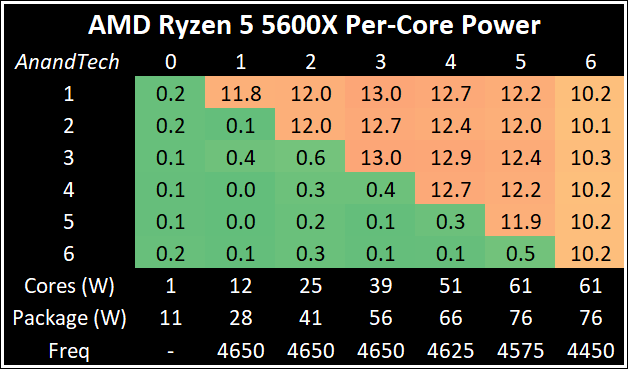
| Ryzen 5 5600X | 4600 | 4625 | 4650 | 3700 | 4450 | 65 | 76 | 10.20 | ||
| *Listed 1T: The official number on the box *Firmware 1T: 'Maximum Frequency' as listed in CPU registers in AGESA 1100 |
||||||||||
The main takeaway from this data, aside from those measured turbo values, is that one of AMD’s new Zen 3 cores can hit 4000 MHz in around 7 W, as indicated by the per core values on the 5950X and 5900X. For the future AMD Milan EPYC enterprise processors, this is vital information to see where exactly some of those processors will end up within any given power budget (such as 225 W or 280 W).
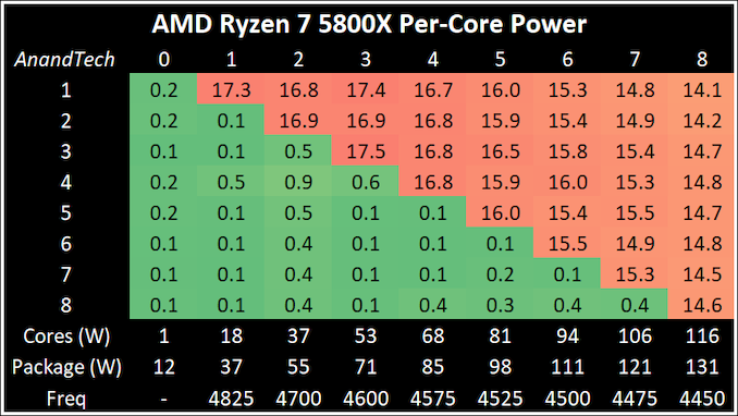
Also of note are the last two processors – both processors are reporting 4450 MHz all-core turbo frequency, however the 5800X is doing it with 14.55 W per core, but the 5600X can do it with only 10.20 W per core. In this instance, this seems that the voltage of the 5800X is a lot higher than the other processors, and this is forcing higher thermals – we were measuring 90ºC at full load after 30 seconds (compared to 73ºC on the 5600X or 64ºC on the 5950X), which might be stunting the frequency here. The motherboard might be over-egging the voltage a little here, going way above what is actually required for the core.
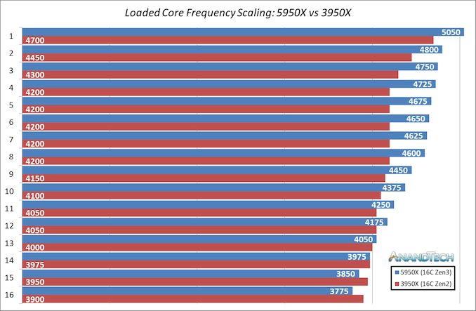
Moving back to the halo chip, we can compare the loaded Core Frequency scaling of the new Ryzen 9 5950X with Zen 3 cores against the previous generation Ryzen 9 3950X with Zen 2 cores. It looks a little something like this.
Note that the 3950X numbers are updated from our original 3950X review, given that there have been a wide variety of BIOS updates since. Both CPUs exhibit a quick drop off from single core loading, and between 3-8 core load it remains steady, with the new processor anywhere from 400-450 MHz higher. As we scale up beyond eight cores, the two parts actually converge at 14-core load, and when we sit at a full CPU, our Ryzen 9 5950X is 125 MHz lower than the 3950X.
Should we look much into this? The listed base frequency of the Ryzen 9 5950X is 100 MHz lower than the Ryzen 9 3950X (3400 MHz vs 3500 MHz), and we’re seeing a 125 MHz all-core difference. This has the potential to indicate that Zen3 has a higher current density when all the cores are active, and due to the characteristics of the silicon and the core design (such as the wider core and faster load/store), there has to be this frequency difference to maintain the power when all cores are loaded. Naturally the benefit of Zen 3 is that higher performance per core, which should easily go beyond the 125 MHz difference. The benchmarks over the next dozen pages will showcase this.
TDP and Power Draw: No Real Surprises
The nature of reporting processor power consumption has become, in part, a dystopian nightmare. Historically the peak power consumption of a processor, as purchased, is given by its Thermal Design Power (TDP, or PL1). For many markets, such as embedded processors, that value of TDP still signifies the peak power consumption. For the processors we test at AnandTech, either desktop, notebook, or enterprise, this is not always the case.
Modern high performance processors implement a feature called Turbo. This allows, usually for a limited time, a processor to go beyond its rated frequency. Exactly how far the processor goes depends on a few factors, such as the Turbo Power Limit (PL2), whether the peak frequency is hard coded, the thermals, and the power delivery. Turbo can sometimes be very aggressive, allowing power values 2.5x above the rated TDP.
AMD and Intel have different definitions for TDP, but are broadly speaking applied the same. The difference comes to turbo modes, turbo limits, turbo budgets, and how the processors manage that power balance. These topics are 10000-12000 word articles in their own right, and we’ve got a few articles worth reading on the topic.
- Why Intel Processors Draw More Power Than Expected: TDP and Turbo Explained
- Talking TDP, Turbo and Overclocking: An Interview with Intel Fellow Guy Therien
- Reaching for Turbo: Aligning Perception with AMD’s Frequency Metrics
- Intel’s TDP Shenanigans Hurts Everyone
In simple terms, processor manufacturers only ever guarantee two values which are tied together - when all cores are running at base frequency, the processor should be running at or below the TDP rating. All turbo modes and power modes above that are not covered by warranty.
For AMD’s new Ryzen 5000 processors, most of them have a 105 W TDP, with a Package Power Tracking (PPT) setting of 142 W. For these processors, we can see our peak power consumption through our testing matching that value. For the sole 65 W processor, the PPT value is 88 W, and we’re seeing only 76 W, showing some of the efficiencies on the Ryzen 5 5600X.
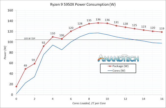
If we look directly at the Ryzen 9 5950X for chip wide power consumption over per-core loading, we get this following graph. Here we are reporting two of the values that we have access to on the chip, which the chip estimates as part of its turbo detection and action algorithms: total package power (for the whole chip), and the power solely used by the sum of cores, which includes the L3 cache. The difference between the two covers the IO die as well as any chiplet-to-chiplet communications, PCIe, CPU-to-chipset, and DRAM controller consumption.
There are two significant features of this graph.
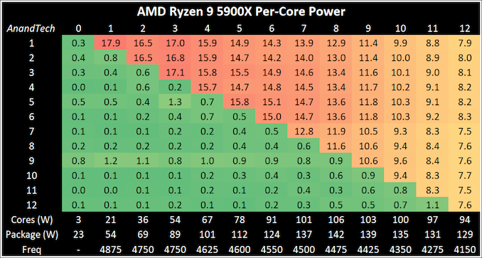
First is the hump, and a slow decrease in total package power consumption after 8-10 core loading. We saw this when we first tested the previous generation 3950X, and is indicative of how the processor has increased current density as it loads up the cores, and as a result there’s a balance between the frequency it can give, delivering the power, and applying the voltage in a consistent way. We’re seeing the difference between the two values also increasing slightly, as more data is transferred over those off-chiplet communications. We see this effect on the 5900X as well, perhaps indicating this is a feature of the dual chiplet design – we’re not seeing it on the 5800X or 5600X.
The second feature is an odd dip in power moving from 4 to 5 cores loaded. Looking into the data, the frequency of the active cores drops from 4725 to 4675, which isn’t a big drop, however the voltage decreases from 1.38 V to 1.31 V, which seems to be more sizeable drop than other voltage readouts as we scale the core-to-core loading. There’s also a bigger increase in non-core power, up from 16 W to 21 W, which perhaps decreases the power to the cores, reducing the voltage.
This might be an odd quirk of our specific chip, our power test, or it might be motherboard or BIOS specific (or a combination of several factors). We might go back in future on other boards to see if this is consistent.
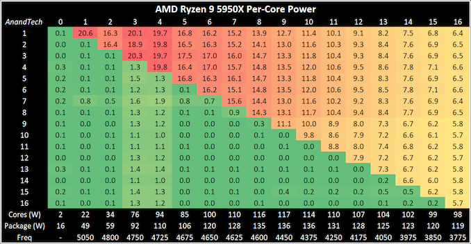
When we dive into per-core power loading, we get the following:
The big chip’s power distribution seems to go up in that 3-4 core loading before coming back down again. But as we load up the second chiplet moving from 8 to 9 core loading, it is worth noting that the second chipset is reporting lower core power, despite showing the same core frequency. AMD is able to supply the two chiplets different amounts of voltage and power, and we might be seeing this play out in real time.
Perhaps very important is that single core power consumption when we are at 5050 MHz of 20.6 W. Going back to our previous generation data, on Zen 2 we were only seeing a peak of 18.3 W, and a slightly higher voltage reported (1.45 V for Zen 2 vs 1.42 V for Zen 3). This means that from the perspective of our two chips, Zen 3 cores scale better in frequency, and even though the power increases as expected, the voltage simultaneously decreases (Note that there can be some silicon variability to also account for some of this.)
Moving down the stack, the 12-core Ryzen 9 5900X doesn’t show any surprises – we’re seeing the same drop off as we load up the cores, this time as we go beyond eight cores. As this processor uses two chiplets, each with six cores, that second set of six cores seem to be consuming lower power per core as we add in additional load.
Some users might be scratching their heads – why is the second chiplet in both of these chips using less power, and therefore being more efficient? Wouldn’t it be better to use that chiplet as the first chiplet for lower power consumption at low loads? I suspect the answer here is nuanced – this first chipet likely has cores that enable a higher leakage profile, and then could arguably hit the higher frequencies at the expense of the power.
Moving down to a single chiplet but will the full power budget, and there is some power savings by not having the communications of a second chiplet. However, at 8-core load, the 5800X is showing 4450 MHz: the Ryzen 9 processors are showing 4475 MHz and 4500 MHz, indicating that there is still some product differentiation going on with this sort of performance. With this chip we still saw 140 W peak power consumption, however it wasn’t on this benchmark (our peak numbers can come from a number of benchmarks we monitor, not just our power-loading benchmark set).
At the 65 W level of the 5600X, as mentioned before, the all-core frequency is 4450 MHz, which is actually 50 MHz behind the 5800X. However this chip is very consistent, still giving up +50 MHz on its peak turbo compared to the on-box number. It also carries this turbo through to at least 3 core loading, and doesn’t lose much to 5 core loading. Users looking for something low power and consistent could be swayed by this chip.
For some specific real-world tests, we’re going to focus solely on the Ryzen 9 5950X. First up is our image-model construction workload, using our Agisoft Photoscan benchmark. This test has a number of different areas that involve single thread, multi-thread, or memory limited algorithms.
Most of this test sits around the 130 W mark, as the workload has a variable thread count. There are a couple of momentary spikes above 140 W, however everything is well within expected parameters.
The second test is from y-Cruncher, which is our AVX2/AVX512 workload. This also has some memory requirements, which can lead to periodic cycling with systems that have lower memory bandwidth per core options.
Our y-Cruncher test often shows one of two patterns – either a flat line for power-limited processors, or this zig-zag as the test is loaded and also uses a good portion of memory transfers for the calculation. Usually it is the latter which showcases when we’re getting the most out of the processor, and we get this here.
Compared to other processors, for peak power, we report the highest loaded value observed from any of our benchmark tests.
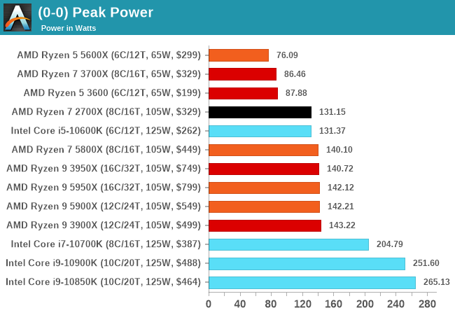
Due to AMD’s PPT implementation, we’re getting very consistent peak power results between multiple generations of AMD processors. Because OEMs play around with Intel’s turbo implementation, essentially to an unlimited peak turbo power, this is why we see full-loaded values well above 200 W. While Intel stays on its most optimized 14nm process and AMD leverages TSMC’s leading 7nm, along with multiple generations of DTCO, AMD will have that efficiency lead.
Section by Andrei Frumusanu
CPU ST Performance: SPEC 2006, SPEC 2017
SPEC2017 and SPEC2006 is a series of standardized tests used to probe the overall performance between different systems, different architectures, different microarchitectures, and setups. The code has to be compiled, and then the results can be submitted to an online database for comparison. It covers a range of integer and floating point workloads, and can be very optimized for each CPU, so it is important to check how the benchmarks are being compiled and run.
We run the tests in a harness built through Windows Subsystem for Linux, developed by our own Andrei Frumusanu. WSL has some odd quirks, with one test not running due to a WSL fixed stack size, but for like-for-like testing is good enough. SPEC2006 is deprecated in favor of 2017, but remains an interesting comparison point in our data. Because our scores aren’t official submissions, as per SPEC guidelines we have to declare them as internal estimates from our part.
For compilers, we use LLVM both for C/C++ and Fortan tests, and for Fortran we’re using the Flang compiler. The rationale of using LLVM over GCC is better cross-platform comparisons to platforms that have only have LLVM support and future articles where we’ll investigate this aspect more. We’re not considering closed-sourced compilers such as MSVC or ICC.
clang version 10.0.0

clang version 7.0.1 (ssh://[email protected]/flang-compiler/flang-driver.git

 24bd54da5c41af04838bbe7b68f830840d47fc03)
-Ofast -fomit-frame-pointer

-march=x86-64

-mtune=core-avx2

-mfma -mavx -mavx2
Our compiler flags are straightforward, with basic –Ofast and relevant ISA switches to allow for AVX2 instructions.
To note, the requirements for the SPEC licence state that any benchmark results from SPEC have to be labelled ‘estimated’ until they are verified on the SPEC website as a meaningful representation of the expected performance. This is most often done by the big companies and OEMs to showcase performance to customers, however is quite over the top for what we do as reviewers.
We start off with SPEC2006, a legacy benchmark by now, but which still has very well understood microarchitectural behaviour for us to analyse the new Zen3 design:
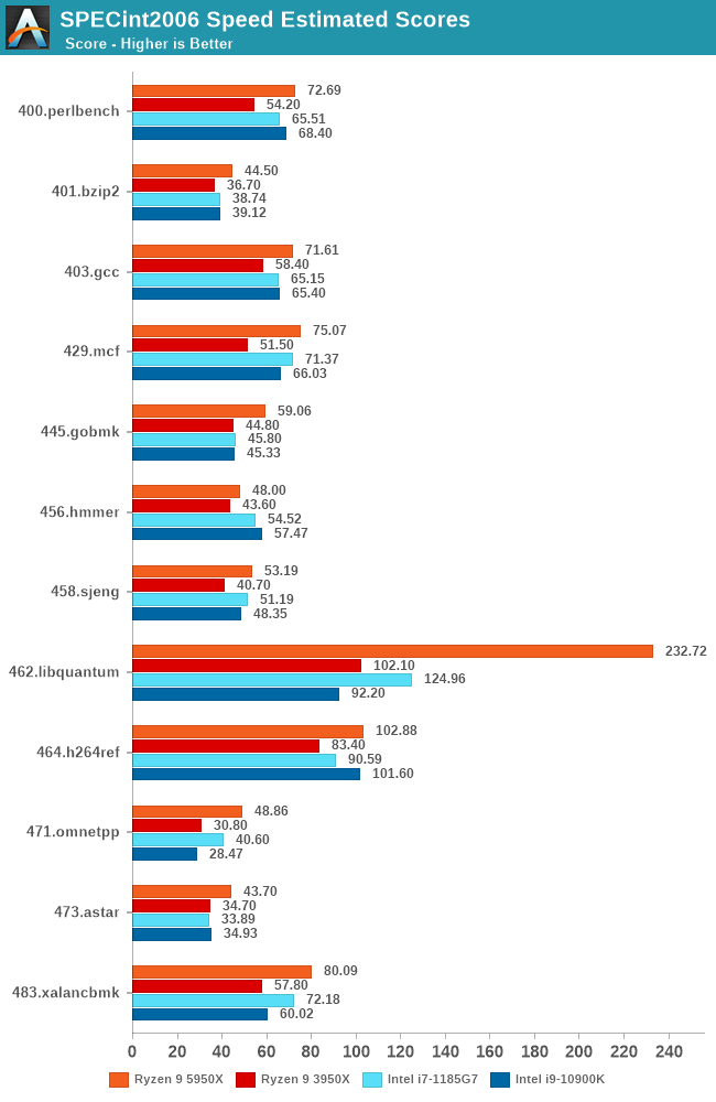
In SPECint2006, we’re seeing healthy performance upticks across the board for many of the tests. Particularly standing out is the new 462.libquantum behaviour of the Ryzen 9 5950X which is posting more than double the performance of its predecessor, likely thanks to the new much larger cache, but also the overall higher load/store throughput of the new core as well as the memory improvements of the microarchitecture.
We’re also seeing very large performance increases for 429.mcf and 471.omnetpp which are memory latency sensitive: Although the new design doesn’t actually change the structural latency to DRAM all that much, the new core’s much improved and smarter handling of memory through new cache-line replacement algorithms, new prefetchers, seem to have a large impact on these workloads.
400.perlbench is interesting as it’s not really a memory-heavy or L3 heavy workload, but instead has a lot of instruction pressure. I think that Zen3’s large boost here might be due to the new optimised OP-cache handling and optimisations as that would make the most sense out of all the changes in the new design – it’s one of the tests that has a very high L1I cache miss rate.
A simpler test that’s solely integer execution bound and sits almost solely in the L1D is 456.hmmer, and here we’re seeing only a minor uplift in performance only linear with the clock frequency increase of the new design, with only a 1% IPC uplift. Given that Zen3 doesn’t actually change its integer execution width in terms of ALUs or overall machine width, it makes sense to not see much improvements here.
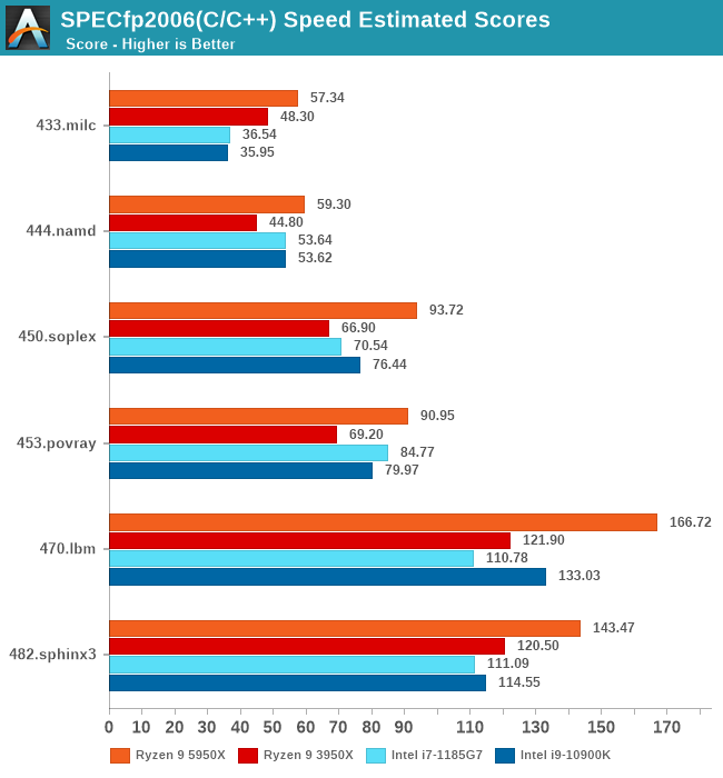
In SPECfp2006, we’re seeing more healthy boosts in performance across the board which is mostly due to the more memory intensive nature of the workloads, and we’re seeing large IPC uplifts in most tests due to the larger L3 as well as the better memory capabilities of the core. 433.milc sees a smaller uplift than the other benchmarks and that’s due to it being more DRAM memory bandwidth bound. 482.spinx is also seeing a smaller 9% IPC uplift due to it not being that memory intensive.
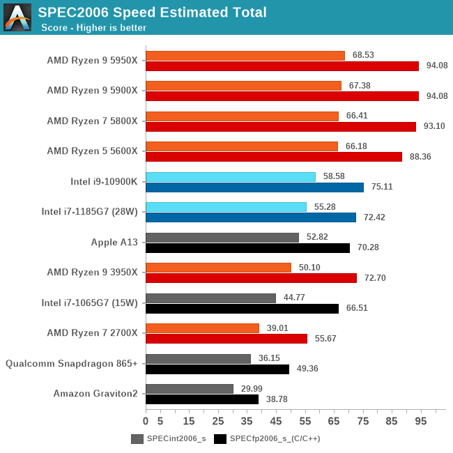
In the overall 2006 scores, the new Ryzen 5000 series parts are showcasing very large generational performance uplifts with margins well beyond that of the previous generation, as well as the nearest competition. Against the 3950X, the new 5950X is 36% faster in the integer workloads, and 29% faster in the floating-point workloads, which are both massive uplifts. AMD is also leaving Intel behind in terms of performance here with a 17% and 25% performance advantage against the 10900K.
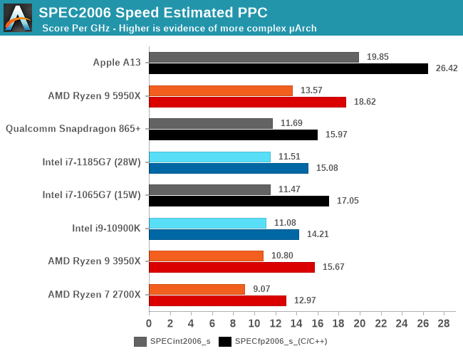
In the performance per clock uplifts, measured at peak performance, we’re seeing a 20.87% median and 24.99% average improvement for the new Zen3 microarchitecture when compared to last year’s Zen2 design. AMD is still quite behind Apple’s A13 and A14 (review coming soon), but that’s natural given the almost double the microarchitectural width of Apple’s design, running at lower frequencies. It’ll be interesting to get Apple Silicon Mac devices tested and compared against the new AMD parts.
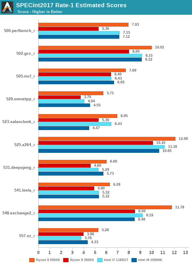
Moving onto the newer SPECint2017, we again see some large improvement of Zen3 depending on the various microarchitectural characteristics of the respective workloads. 500.perlbench_r again shows a massive 37% IPC uplift for the new architecture – again very likely to the new design and optimisations on the part of the OP-cache of the Zen3 design.
520.omnetpp again also shows a 42% IPC uplift thanks to the memory technologies employed in the new design. Execution throughput limited workloads such as 525.x264 are seeing smaller increases of 9.5% IPC due to again overall less changes on this aspect of the microarchitecture.
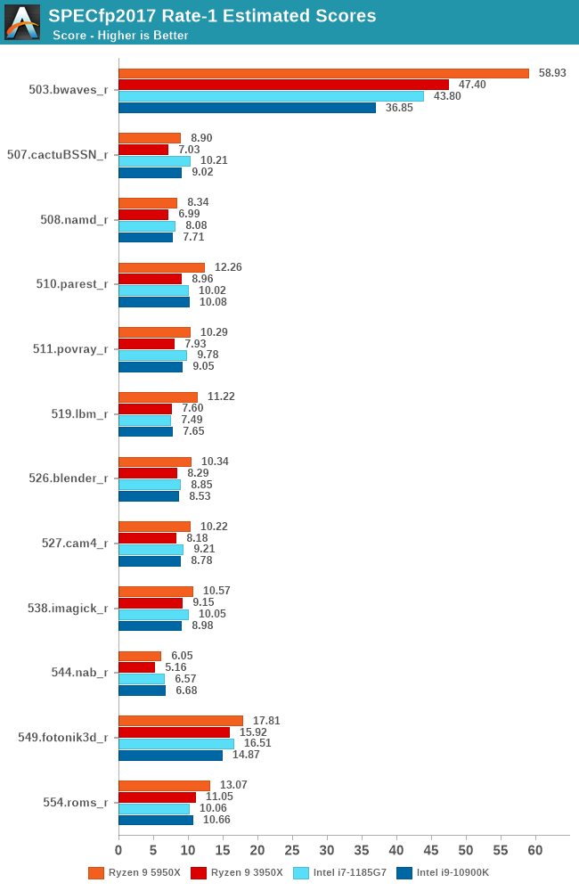
In SPECfp2017, we see a similar situation as previous workloads. Execution-bound workloads such as 508.namd or 538.imagick are seeing smaller IPC increases in the 9-6% range. Similarly, DRAM bandwidth starved workloads such as 549.fotonik3d and 554.roms are showcasing also smaller IPC boosts of 2.7 – 8.6%.
The more hybrid workloads which make good use of the caches are seeing larger performance improvements across the board. Up to a 35.6% IPC peak for 519.lbm.
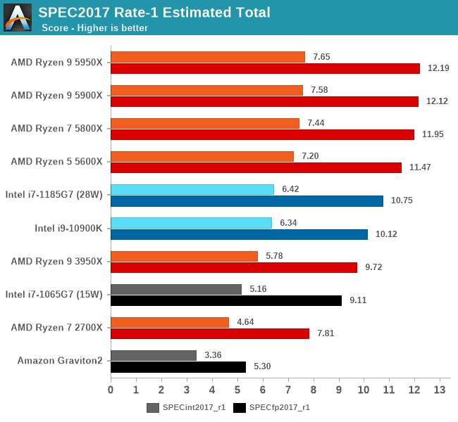
In the SPEC2017 suite total performance figures, the new Ryzen 5000 also shine thanks to their frequency and IPC uplifts. Generationally, across the int2017 and fp2017 suites, we’re seeing a 32% and 25% performance boost over the 3950X, which are very impressive figures.
IPC wise, looking at a histogram of all SPEC workloads, we’re seeing a median of 18.86%, which is very near AMD’s proclaimed 19% figure, and an average of 21.38% - although if we discount libquantum that average does go down to 19.12%. AMD’s marketing numbers are thus pretty much validated as they’ve exactly hit their proclaimed figure with the new Zen3 microarchitecture.
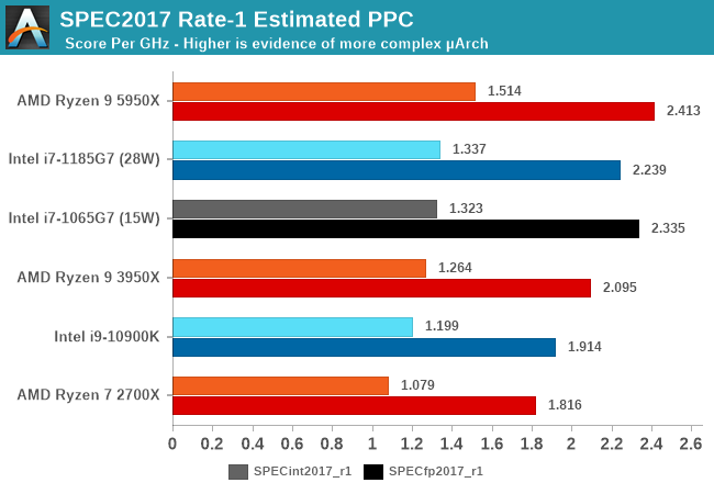
On the competitive landscape, this now makes Zen3 the undisputed leader in the x86 space, leaving Intel’s old Skylake designs far behind and also showing more design complexity than the newer Sunny Cove and Willow Cove cores.
Overall, the new Ryzen 5000 series and the Zen3 microarchitecture seem like absolute winners, and there’s no dispute about them taking the performance crown. AMD has achieved this through both an uplift in frequency, as well as a notable 19% uplift thanks to a smarter design.
What I hope to see from AMD in future designs is a more aggressive push towards a wider core design with even larger IPC jumps. In workloads that are more execution bound, Zen3 isn’t all that big of an uplift. The move from a 16MB to a 32MB L3 cache isn’t something that’ll repeated any time soon in terms of improvement magnitude, and it’s also very doubtful we’ll see significant frequency uplifts with coming generations. As Moore’s Law is slowing, going wider and smarter seems to be the only way forward for advancing performance.
Section by Andrei Frumusanu
CPU MT Performance: SPEC 2017
Whilst single-threaded performance of Zen3 seems to be an absolute win for the new Ryzen 5000 series CPUs, multi-threaded performance is also the other important aspect of a design. Generally, what comes into play much more for multi-threaded performance is the power efficiency of the design. As none of the current x86 consumer or enterprise parts are able to actually run all their cores at maximum frequency for peak performance due to platform power limitations, any resulting performance boost we might see between generations with a similar power cap will be due to power and energy efficiency gains between the designs.
For AMD, we’re limiting the detailed comparisons here to the 3950X and the 5950X which both have a PPT of 142W, which means that’s the maximum peak power for the platform, and observed 120-125W sustained figures in actual workloads. We’re also throwing in a 10900K for context, but given the very different core count numbers it doesn’t serve an exact apples-to-apples comparison.
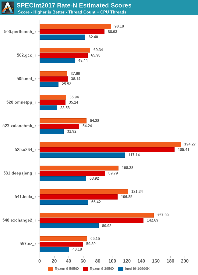
Starting off with SPECint2006, the performance uplifts for the new Ryzen 5000 series here doesn’t seem to be all that significant in most tests, with uplifts well below those of the single-thread benchmarks.
Most of the tests are showing a 10% performance uplift, with the more memory heavy test showing no improvement. Some of the minor uplifts such as a 5% boost in 502.gcc seem quite disappointing and showcase that the new platform isn’t all that big of a boost for productivity workloads.
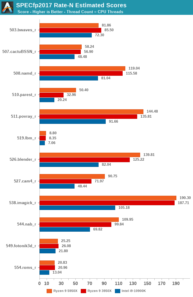
In SPECfp2017, 510.parest and 527.cam4 stand out as the two workloads with the biggest improvements, with the rest of the workloads all either having sub-5% improvements, or even just flat or slower performance than the 3950X.
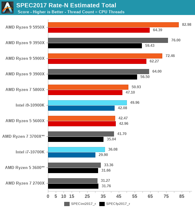
** Preliminary figures to be re-tested due to 2x16GB SR vs 4x8GB SR memory DIMM configuration, scores will improve.
Overall, the new Ryzen 5000 series are showcasing a quite conservative 8-9% performance improvement over their predecessor generation SKUs. The 12-core variant here is showing a little bigger boost of 10-13%.
In this regard, the new chips seem to have missed the mark in terms of AMD’s claims for 12% better performance per watt for the new 5950X, and 26% better performance per watt for the 5900X – their marketing should have done better in explaining those figures, or just be more conservative with their numbers. This also doesn’t bode too well for the eventual EPYC-based Zen3 Milan chips.
Test Setup and #CPUOverload Benchmarks
As per our processor testing policy, we take a premium category motherboard suitable for the socket, and equip the system with a suitable amount of memory running at the manufacturer's maximum supported frequency. This is also typically run at JEDEC subtimings where possible. It is noted that some users are not keen on this policy, stating that sometimes the maximum supported frequency is quite low, or faster memory is available at a similar price, or that the JEDEC speeds can be prohibitive for performance. While these comments make sense, ultimately very few users apply memory profiles (either XMP or other) as they require interaction with the BIOS, and most users will fall back on JEDEC supported speeds - this includes home users as well as industry who might want to shave off a cent or two from the cost or stay within the margins set by the manufacturer. Where possible, we will extend out testing to include faster memory modules either at the same time as the review or a later date.
| AnandTech | Example Processors |
Motherboard | DRAM | PSU | SSD |
| AMD | |||||
| Zen 3 CPU | Ryzen 9 5950X | MSI X570 Godlike (1.B3T13) |
Corsair RGB Dominator Pro 32 GB DDR4-3200 |
OCZ Gold 1250W |
Crucial MX500 2 TB |
| Ryzen 9 5900X | |||||
| Ryzen 7 5800X | |||||
| Ryzen 5 5600X | |||||
| Zen 2 CPU | Ryzen 9 3950X | GIGABYTE X570 Aorus I Pro (F30a) |
ADATA 32 GB DDR4-3200 |
Corsair AX860i |
Crucial MX500 2 TB |
| Ryzen 9 3900X | |||||
| Ryzen 7 3800XT | |||||
| Ryzen 7 3700X | |||||
| Ryzen 5 3600 | |||||
| Zen+ CPU | Ryzen 7 2700X | GIGABYTE X570 Aorus I Pro (F30a) |
ADATA 32 GB DDR4-3200 |
Corsair AX860i |
Crucial MX500 2 TB |
| Intel | |||||
| Comet Lake CPU |
Core i9-10900K | ASRock Z490 PG Velocia |
Corsair RGB Dominator Pro 32 GB DDR4-2933 |
OCZ Gold 1250 W |
Crucial MX500 2 TB |
| Core i9-10850K | |||||
| Core i7-10700K | |||||
| Core i5-10600K | |||||
Many thanks to...
We must thank the following companies for kindly providing hardware for our multiple test beds. Some of this hardware is not in this test bed specifically, but is used in other testing.
| Hardware Providers for CPU and Motherboard Reviews | |||
| Sapphire RX 460 Nitro |
NVIDIA RTX 2080 Ti |
Crucial SSDs | Corsair PSUs |
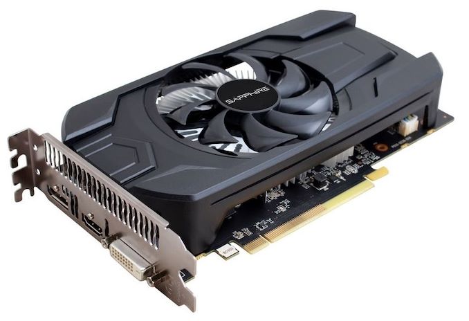 |
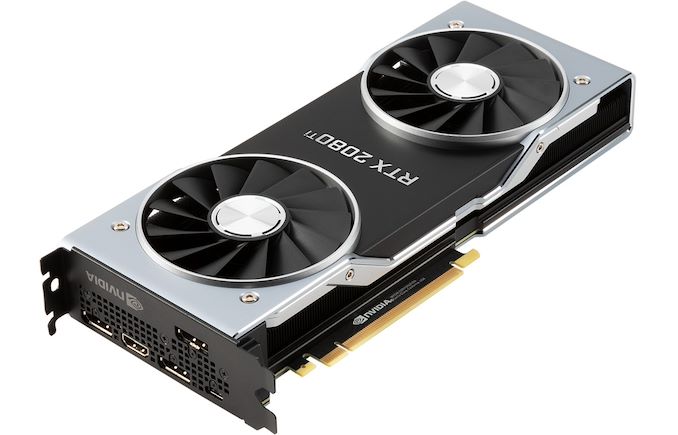 |
 |
 |
| G.Skill DDR4 | ADATA DDR4 | Silverstone Coolers |
Noctua Coolers |
 |
 |
 |
|
-
The 2020 #CPUOverload Suite
Our CPU tests go through a number of main areas. We cover Web tests using our un-updateable version of Chromium, opening tricky PDFs, emulation, brain simulation, AI, 2D image to 3D model conversion, rendering (ray tracing, modeling), encoding (compression, AES, video and HEVC), office based tests, and our legacy tests (throwbacks from another generation of code but interesting to compare).
The Win10 Pro operating system is prepared in advance, and we run a number of registry edit commands again to ensure that various system features are turned off and disabled at the start of the benchmark suite. This includes disabling Cortana, disabling the GameDVR functionality, disabling Windows Error Reporting, disabling Windows Defender as much as possible again, disabling updates, and re-implementing power options and removing OneDrive, in-case it sprouted wings again.
A number of these tests have been requested by our readers, and we’ve split our tests into a few more categories than normal as our readers have been requesting specific focal tests for their workloads. A recent run on a Core i5-10600K, just for the CPU tests alone, took around 20 hours to complete.
Power
- Peak Power (y-Cruncher using latest AVX)
- Per-Core Loading Power using POV-Ray
Office
- Agisoft Photoscan 1.3: 2D to 3D Conversion
- Application Loading Time: GIMP 2.10.18 from a fresh install
- Compile Testing (WIP)
Science
- 3D Particle Movement v2.1 (Non-AVX + AVX2/AVX512)
- y-Cruncher 0.78.9506 (Optimized Binary Splitting Compute for mathematical constants)
- NAMD 2.13: Nanoscale Molecular Dynamics on ApoA1 protein
- AI Benchmark 0.1.2 using TensorFlow (unoptimized for Windows)
Simulation
- Digicortex 1.35: Brain stimulation simulation
- Dwarf Fortress 0.44.12: Fantasy world creation and time passage
- Dolphin 5.0: Ray Tracing rendering test for Wii emulator
Rendering
- Blender 2.83 LTS: Popular rendering program, using PartyTug frame render
- Corona 1.3: Ray Tracing Benchmark
- Crysis CPU-Only: Can it run Crysis? What, on just the CPU at 1080p? Sure
- POV-Ray 3.7.1: Another Ray Tracing Test
- V-Ray: Another popular renderer
- CineBench R20: Cinema4D Rendering engine
Encoding
- Handbrake 1.32: Popular Transcoding tool
- 7-Zip: Open source compression software
- AES Encoding: Instruction accelerated encoding
- WinRAR 5.90: Popular compression tool
Legacy
- CineBench R10
- CineBench R11.5
- CineBench R15
- 3DPM v1: Naïve version of 3DPM v2.1 with no acceleration
- X264 HD3.0: Vintage transcoding benchmark
Web
- Kraken 1.1: Depreciated web test with no successor
- Octane 2.0: More comprehensive test (but also deprecated with no successor)
- Speedometer 2: List-based web-test with different frameworks
Synthetic
- GeekBench 4 and GeekBench 5
- AIDA Memory Bandwidth
- Linux OpenSSL Speed (rsa2048 sign/verify, sha256, md5)
- LinX 0.9.5 LINPACK (where appropriate)
SPEC (Estimated)
- SPEC2006 rate-1T
- SPEC2017 rate-1T
- SPEC2017 rate-nT
It should be noted that due to the terms of the SPEC license, because our benchmark results are not vetted directly by the SPEC consortium, we have to label them as ‘estimated’. The benchmark is still run and we get results out, but those results have to have the ‘estimated’ label.
Others
- A full x86 instruction throughput/latency analysis
- Core-to-Core Latency
- Cache-to-DRAM Latency
- Frequency Ramping
Some of these tests also have AIDA power wrappers around them in order to provide an insight in the way the power is reported through the test.
2020 CPU Gaming (GPU) Benchmarks
In the past, we’ve tackled the GPU benchmark set in several different ways. We’ve had one GPU to multiple games at one resolution, or multiple GPUs take a few games at one resolution, then as the automation progressed into something better, multiple GPUs take a few games at several resolutions. However, based on feedback, having the best GPU we can get hold of over a dozen games at several resolutions seems to be the best bet.
Normally securing GPUs for this testing is difficult, as we need several identical models for concurrent testing, and very rarely is a GPU manufacturer, or one of its OEM partners, happy to hand me 3-4+ of the latest and greatest. In that aspect, over the years, I have to thank ECS for sending us four GTX 580s in 2012, MSI for sending us three GTX 770 Lightnings in 2014, Sapphire for sending us multiple RX 480s and R9 Fury X cards in 2016, and in our last test suite, MSI for sending us three GTX 1080 Gaming cards in 2018.
For our testing on the 2020 suite, we have secured three RTX 2080 Ti GPUs direct from NVIDIA. These GPUs have been optimized for with drivers and in gaming titles, and given how rare our updates are, we are thankful for getting the high-end hardware. (It’s worth noting we won’t be updating to whatever RTX 3080 variant is coming out at some point for a while yet.)
On the topic of resolutions, this is something that has been hit and miss for us in the past. Some users state that they want to see the lowest resolution and lowest fidelity options, because this puts the most strain on the CPU, such as a 480p Ultra Low setting. In the past we have found this unrealistic for all use cases, and even if it does give the best shot for a difference in results, the actual point where you come GPU limited might be at a higher resolution. In our last test suite, we went from the 720p Ultra Low up to 1080p Medium, 1440p High, and 4K Ultra settings. However, our most vocal readers hated it, because even by 1080p medium, we were GPU limited for the most part.
So to that end, the benchmarks this time round attempt to follow the basic pattern where possible:
- Lowest Resolution with lowest scaling, Lowest Settings
- 2560x1440 with the lowest settings (1080p where not possible)
- 3840x2160 with the lowest settings
- 1920x1080 at the maximum settings
Point (1) should give the ultimate CPU limited scenario. We should see that lift as we move up through (2) 1440p and (3) 4K, with 4K low still being quite strenuous in some titles.
Point (4) is essentially our ‘real world’ test. The RTX 2080 Ti is overkill for 1080p Maximum, and we’ll see that most modern CPUs pull well over 60 FPS average in this scenario.
What will be interesting is that for some titles, 4K Low is more compute heavy than 1080p Maximum, and for other titles that relationship is reversed.
For integrated graphics testing, we use the (1) and (4) settings to see where the GPU lies with respect to CPU performance (1) as well as test to confirm just how close integrated graphics is to proper 1080p gaming (4).
So we have the following benchmarks as part of our script, automated to the point of a one-button run and out pops the results approximately 10 hours later, per GPU. Also listed are the resolutions and settings used.
Offline Games
- Chernobylite, 360p Low, 1440p Low, 4K Low, 1080p Max
- Civilization 6, 480p Low, 1440p Low, 4K Low, 1080p Max
- Deus Ex: Mankind Divided, 600p Low, 1440p Low, 4K Low, 1080p Max
- Final Fantasy XIV: 768p Min, 1440p Min, 4K Min, 1080p Max
- Final Fantasy XV: 720p Standard, 1080p Standard, 4K Standard, 8K Standard
- World of Tanks: 768p Min, 1080p Standard, 1080p Max, 4K Max
Online Games
- Borderlands 3, 360p VLow, 1440p VLow, 4K VLow, 1080p Badass
- F1 2019, 768p ULow, 1440p ULow, 4K ULow, 1080p Ultra
- Far Cry 5, 720p Low, 1440p Low, 4K Low, 1080p Ultra
- Gears Tactics, 720p Low, 4K Low, 8K Low 1080p Ultra
- Grand Theft Auto 5, 720p Low, 1440p Low, 4K Low, 1080p Max
- Red Dead Redemption 2, 384p Min, 1440p Min, 8K Min, 1080p Max
- Strange Brigade DX12, 720p Low, 1440p Low, 4K Low, 1080p Ultra
- Strange Brigade Vulkan, 720p Low, 1440p Low, 4K Low, 1080p Ultra
For each of the games in our testing, we take the frame times where we can (the two that we cannot are Chernobylite and FFXIV). For these games, at each resolution/setting combination, we run them for as many loops in a given time limit (often 10 minutes per resolution). Results are then taken as average frame rates and 95th percentiles.
If there are any game developers out there involved with any of the benchmarks above, please get in touch at [email protected]. I have a list of requests to make benchmarking your title easier! I have a literal document I’ve compiled showing what would be ideal, best practices, who gets it correct and who gets it wrong, etc.
The other angle is DRM, and some titles have limits of 5 systems per day. This may limit our testing in some cases; in other cases it is solvable.
CPU Tests: Office and Science
Our previous set of ‘office’ benchmarks have often been a mix of science and synthetics, so this time we wanted to keep our office section purely on real world performance.
Agisoft Photoscan 1.3.3: link
The concept of Photoscan is about translating many 2D images into a 3D model - so the more detailed the images, and the more you have, the better the final 3D model in both spatial accuracy and texturing accuracy. The algorithm has four stages, with some parts of the stages being single-threaded and others multi-threaded, along with some cache/memory dependency in there as well. For some of the more variable threaded workload, features such as Speed Shift and XFR will be able to take advantage of CPU stalls or downtime, giving sizeable speedups on newer microarchitectures.
For the update to version 1.3.3, the Agisoft software now supports command line operation. Agisoft provided us with a set of new images for this version of the test, and a python script to run it. We’ve modified the script slightly by changing some quality settings for the sake of the benchmark suite length, as well as adjusting how the final timing data is recorded. The python script dumps the results file in the format of our choosing. For our test we obtain the time for each stage of the benchmark, as well as the overall time.
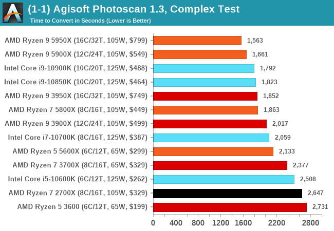
Application Opening: GIMP 2.10.18
First up is a test using a monstrous multi-layered xcf file to load GIMP. While the file is only a single ‘image’, it has so many high-quality layers embedded it was taking north of 15 seconds to open and to gain control on the mid-range notebook I was using at the time.
What we test here is the first run - normally on the first time a user loads the GIMP package from a fresh install, the system has to configure a few dozen files that remain optimized on subsequent opening. For our test we delete those configured optimized files in order to force a ‘fresh load’ each time the software in run. As it turns out, GIMP does optimizations for every CPU thread in the system, which requires that higher thread-count processors take a lot longer to run.
We measure the time taken from calling the software to be opened, and until the software hands itself back over to the OS for user control. The test is repeated for a minimum of ten minutes or at least 15 loops, whichever comes first, with the first three results discarded.
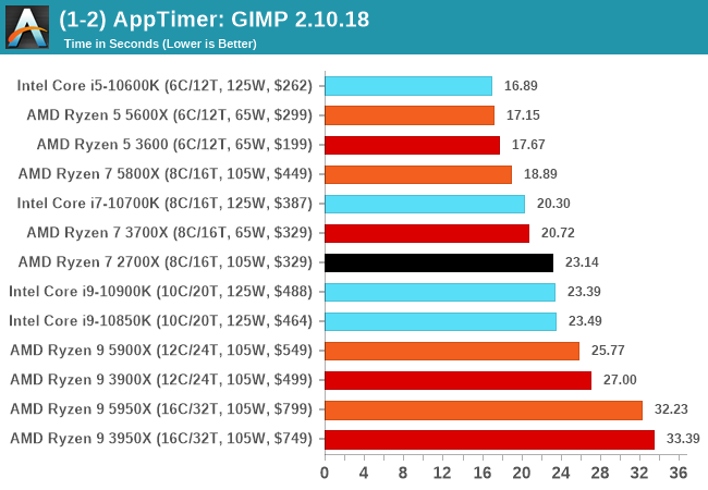
Science
In this version of our test suite, all the science focused tests that aren’t ‘simulation’ work are now in our science section. This includes Brownian Motion, calculating digits of Pi, molecular dynamics, and for the first time, we’re trialing an artificial intelligence benchmark, both inference and training, that works under Windows using python and TensorFlow. Where possible these benchmarks have been optimized with the latest in vector instructions, except for the AI test – we were told that while it uses Intel’s Math Kernel Libraries, they’re optimized more for Linux than for Windows, and so it gives an interesting result when unoptimized software is used.
3D Particle Movement v2.1: Non-AVX and AVX2/AVX512
This is the latest version of this benchmark designed to simulate semi-optimized scientific algorithms taken directly from my doctorate thesis. This involves randomly moving particles in a 3D space using a set of algorithms that define random movement. Version 2.1 improves over 2.0 by passing the main particle structs by reference rather than by value, and decreasing the amount of double->float->double recasts the compiler was adding in.
The initial version of v2.1 is a custom C++ binary of my own code, and flags are in place to allow for multiple loops of the code with a custom benchmark length. By default this version runs six times and outputs the average score to the console, which we capture with a redirection operator that writes to file.
For v2.1, we also have a fully optimized AVX2/AVX512 version, which uses intrinsics to get the best performance out of the software. This was done by a former Intel AVX-512 engineer who now works elsewhere. According to Jim Keller, there are only a couple dozen or so people who understand how to extract the best performance out of a CPU, and this guy is one of them. To keep things honest, AMD also has a copy of the code, but has not proposed any changes.
The 3DPM test is set to output millions of movements per second, rather than time to complete a fixed number of movements.

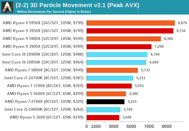
y-Cruncher 0.78.9506: www.numberworld.org/y-cruncher
If you ask anyone what sort of computer holds the world record for calculating the most digits of pi, I can guarantee that a good portion of those answers might point to some colossus super computer built into a mountain by a super-villain. Fortunately nothing could be further from the truth – the computer with the record is a quad socket Ivy Bridge server with 300 TB of storage. The software that was run to get that was y-cruncher.
Built by Alex Yee over the last part of a decade and some more, y-Cruncher is the software of choice for calculating billions and trillions of digits of the most popular mathematical constants. The software has held the world record for Pi since August 2010, and has broken the record a total of 7 times since. It also holds records for e, the Golden Ratio, and others. According to Alex, the program runs around 500,000 lines of code, and he has multiple binaries each optimized for different families of processors, such as Zen, Ice Lake, Sky Lake, all the way back to Nehalem, using the latest SSE/AVX2/AVX512 instructions where they fit in, and then further optimized for how each core is built.
For our purposes, we’re calculating Pi, as it is more compute bound than memory bound. In multithreaded mode we go for 2.5 billion digits. That 2.5 billion digit value requires ~12 GB of DRAM, and so is limited to systems with at least 16 GB.
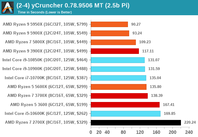
NAMD 2.13 (ApoA1): Molecular Dynamics
One of the popular science fields is modeling the dynamics of proteins. By looking at how the energy of active sites within a large protein structure over time, scientists behind the research can calculate required activation energies for potential interactions. This becomes very important in drug discovery. Molecular dynamics also plays a large role in protein folding, and in understanding what happens when proteins misfold, and what can be done to prevent it. Two of the most popular molecular dynamics packages in use today are NAMD and GROMACS.
NAMD, or Nanoscale Molecular Dynamics, has already been used in extensive Coronavirus research on the Frontier supercomputer. Typical simulations using the package are measured in how many nanoseconds per day can be calculated with the given hardware, and the ApoA1 protein (92,224 atoms) has been the standard model for molecular dynamics simulation.
Luckily the compute can home in on a typical ‘nanoseconds-per-day’ rate after only 60 seconds of simulation, however we stretch that out to 10 minutes to take a more sustained value, as by that time most turbo limits should be surpassed. The simulation itself works with 2 femtosecond timesteps. We use version 2.13 as this was the recommended version at the time of integrating this benchmark into our suite. The latest nightly builds we’re aware have started to enable support for AVX-512, however due to consistency in our benchmark suite, we are retaining with 2.13. Other software that we test with has AVX-512 acceleration.
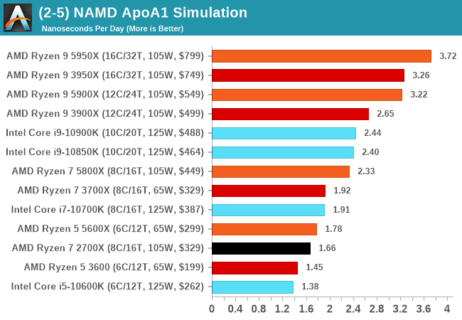
AI Benchmark 0.1.2 using TensorFlow: Link
Finding an appropriate artificial intelligence benchmark for Windows has been a holy grail of mine for quite a while. The problem is that AI is such a fast moving, fast paced word that whatever I compute this quarter will no longer be relevant in the next, and one of the key metrics in this benchmarking suite is being able to keep data over a long period of time. We’ve had AI benchmarks on smartphones for a while, given that smartphones are a better target for AI workloads, but it also makes some sense that everything on PC is geared towards Linux as well.
Thankfully however, the good folks over at ETH Zurich in Switzerland have converted their smartphone AI benchmark into something that’s useable in Windows. It uses TensorFlow, and for our benchmark purposes we’ve locked our testing down to TensorFlow 2.10, AI Benchmark 0.1.2, while using Python 3.7.6.
The benchmark runs through 19 different networks including MobileNet-V2, ResNet-V2, VGG-19 Super-Res, NVIDIA-SPADE, PSPNet, DeepLab, Pixel-RNN, and GNMT-Translation. All the tests probe both the inference and the training at various input sizes and batch sizes, except the translation that only does inference. It measures the time taken to do a given amount of work, and spits out a value at the end.
There is one big caveat for all of this, however. Speaking with the folks over at ETH, they use Intel’s Math Kernel Libraries (MKL) for Windows, and they’re seeing some incredible drawbacks. I was told that MKL for Windows doesn’t play well with multiple threads, and as a result any Windows results are going to perform a lot worse than Linux results. On top of that, after a given number of threads (~16), MKL kind of gives up and performance drops of quite substantially.
So why test it at all? Firstly, because we need an AI benchmark, and a bad one is still better than not having one at all. Secondly, if MKL on Windows is the problem, then by publicizing the test, it might just put a boot somewhere for MKL to get fixed. To that end, we’ll stay with the benchmark as long as it remains feasible.
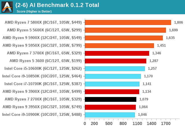
CPU Tests: Simulation
Simulation and Science have a lot of overlap in the benchmarking world, however for this distinction we’re separating into two segments mostly based on the utility of the resulting data. The benchmarks that fall under Science have a distinct use for the data they output – in our Simulation section, these act more like synthetics but at some level are still trying to simulate a given environment.
DigiCortex v1.35: link
DigiCortex is a pet project for the visualization of neuron and synapse activity in the brain. The software comes with a variety of benchmark modes, and we take the small benchmark which runs a 32k neuron/1.8B synapse simulation, similar to a small slug.
The results on the output are given as a fraction of whether the system can simulate in real-time, so anything above a value of one is suitable for real-time work. The benchmark offers a 'no firing synapse' mode, which in essence detects DRAM and bus speed, however we take the firing mode which adds CPU work with every firing.
The software originally shipped with a benchmark that recorded the first few cycles and output a result. So while fast multi-threaded processors this made the benchmark last less than a few seconds, slow dual-core processors could be running for almost an hour. There is also the issue of DigiCortex starting with a base neuron/synapse map in ‘off mode’, giving a high result in the first few cycles as none of the nodes are currently active. We found that the performance settles down into a steady state after a while (when the model is actively in use), so we asked the author to allow for a ‘warm-up’ phase and for the benchmark to be the average over a second sample time.
For our test, we give the benchmark 20000 cycles to warm up and then take the data over the next 10000 cycles seconds for the test – on a modern processor this takes 30 seconds and 150 seconds respectively. This is then repeated a minimum of 10 times, with the first three results rejected. Results are shown as a multiple of real-time calculation.
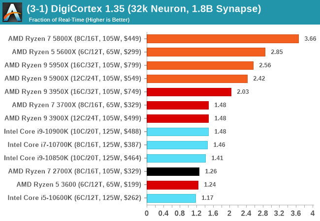
Dwarf Fortress 0.44.12: Link
Another long standing request for our benchmark suite has been Dwarf Fortress, a popular management/roguelike indie video game, first launched in 2006 and still being regularly updated today, aiming for a Steam launch sometime in the future.
Emulating the ASCII interfaces of old, this title is a rather complex beast, which can generate environments subject to millennia of rule, famous faces, peasants, and key historical figures and events. The further you get into the game, depending on the size of the world, the slower it becomes as it has to simulate more famous people, more world events, and the natural way that humanoid creatures take over an environment. Like some kind of virus.
For our test we’re using DFMark. DFMark is a benchmark built by vorsgren on the Bay12Forums that gives two different modes built on DFHack: world generation and embark. These tests can be configured, but range anywhere from 3 minutes to several hours. After analyzing the test, we ended up going for three different world generation sizes:
- Small, a 65x65 world with 250 years, 10 civilizations and 4 megabeasts
- Medium, a 127x127 world with 550 years, 10 civilizations and 4 megabeasts
- Large, a 257x257 world with 550 years, 40 civilizations and 10 megabeasts
DFMark outputs the time to run any given test, so this is what we use for the output. We loop the small test for as many times possible in 10 minutes, the medium test for as many times in 30 minutes, and the large test for as many times in an hour.
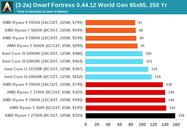
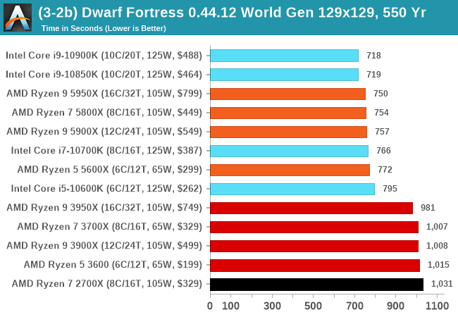
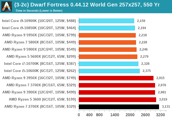
Dolphin v5.0 Emulation: Link
Many emulators are often bound by single thread CPU performance, and general reports tended to suggest that Haswell provided a significant boost to emulator performance. This benchmark runs a Wii program that ray traces a complex 3D scene inside the Dolphin Wii emulator. Performance on this benchmark is a good proxy of the speed of Dolphin CPU emulation, which is an intensive single core task using most aspects of a CPU. Results are given in seconds, where the Wii itself scores 1051 seconds.
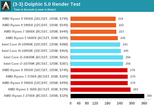
CPU Tests: Rendering
Rendering tests, compared to others, are often a little more simple to digest and automate. All the tests put out some sort of score or time, usually in an obtainable way that makes it fairly easy to extract. These tests are some of the most strenuous in our list, due to the highly threaded nature of rendering and ray-tracing, and can draw a lot of power. If a system is not properly configured to deal with the thermal requirements of the processor, the rendering benchmarks is where it would show most easily as the frequency drops over a sustained period of time. Most benchmarks in this case are re-run several times, and the key to this is having an appropriate idle/wait time between benchmarks to allow for temperatures to normalize from the last test.
Blender 2.83 LTS: Link
One of the popular tools for rendering is Blender, with it being a public open source project that anyone in the animation industry can get involved in. This extends to conferences, use in films and VR, with a dedicated Blender Institute, and everything you might expect from a professional software package (except perhaps a professional grade support package). With it being open-source, studios can customize it in as many ways as they need to get the results they require. It ends up being a big optimization target for both Intel and AMD in this regard.
For benchmarking purposes, we fell back to one rendering a frame from a detailed project. Most reviews, as we have done in the past, focus on one of the classic Blender renders, known as BMW_27. It can take anywhere from a few minutes to almost an hour on a regular system. However now that Blender has moved onto a Long Term Support model (LTS) with the latest 2.83 release, we decided to go for something different.
We use this scene, called PartyTug at 6AM by Ian Hubert, which is the official image of Blender 2.83. It is 44.3 MB in size, and uses some of the more modern compute properties of Blender. As it is more complex than the BMW scene, but uses different aspects of the compute model, time to process is roughly similar to before. We loop the scene for at least 10 minutes, taking the average time of the completions taken. Blender offers a command-line tool for batch commands, and we redirect the output into a text file.
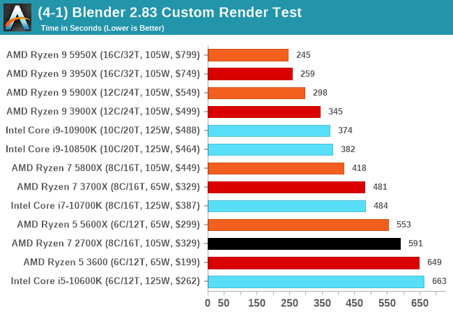
Corona 1.3: Link
Corona is billed as a popular high-performance photorealistic rendering engine for 3ds Max, with development for Cinema 4D support as well. In order to promote the software, the developers produced a downloadable benchmark on the 1.3 version of the software, with a ray-traced scene involving a military vehicle and a lot of foliage. The software does multiple passes, calculating the scene, geometry, preconditioning and rendering, with performance measured in the time to finish the benchmark (the official metric used on their website) or in rays per second (the metric we use to offer a more linear scale).
The standard benchmark provided by Corona is interface driven: the scene is calculated and displayed in front of the user, with the ability to upload the result to their online database. We got in contact with the developers, who provided us with a non-interface version that allowed for command-line entry and retrieval of the results very easily. We loop around the benchmark five times, waiting 60 seconds between each, and taking an overall average. The time to run this benchmark can be around 10 minutes on a Core i9, up to over an hour on a quad-core 2014 AMD processor or dual-core Pentium.
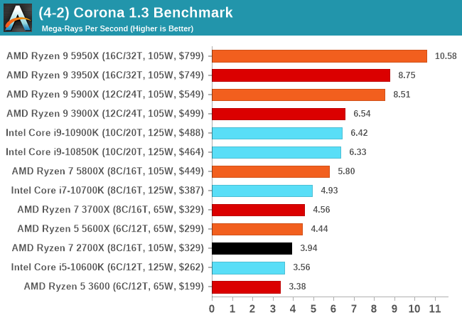
Crysis CPU-Only Gameplay
One of the most oft used memes in computer gaming is ‘Can It Run Crysis?’. The original 2007 game, built in the Crytek engine by Crytek, was heralded as a computationally complex title for the hardware at the time and several years after, suggesting that a user needed graphics hardware from the future in order to run it. Fast forward over a decade, and the game runs fairly easily on modern GPUs.
But can we also apply the same concept to pure CPU rendering? Can a CPU, on its own, render Crysis? Since 64 core processors entered the market, one can dream. So we built a benchmark to see whether the hardware can.
For this test, we’re running Crysis’ own GPU benchmark, but in CPU render mode. This is a 2000 frame test, with medium and low settings.
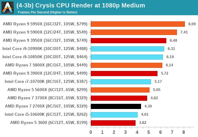
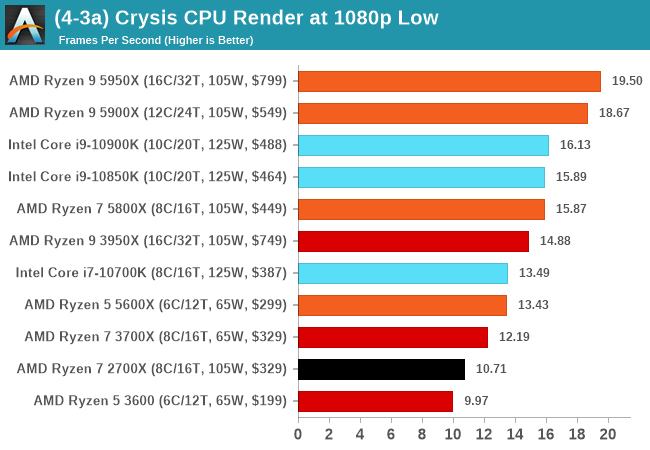
POV-Ray 3.7.1: Link
A long time benchmark staple, POV-Ray is another rendering program that is well known to load up every single thread in a system, regardless of cache and memory levels. After a long period of POV-Ray 3.7 being the latest official release, when AMD launched Ryzen the POV-Ray codebase suddenly saw a range of activity from both AMD and Intel, knowing that the software (with the built-in benchmark) would be an optimization tool for the hardware.
We had to stick a flag in the sand when it came to selecting the version that was fair to both AMD and Intel, and still relevant to end-users. Version 3.7.1 fixes a significant bug in the early 2017 code that was advised against in both Intel and AMD manuals regarding to write-after-read, leading to a nice performance boost.
The benchmark can take over 20 minutes on a slow system with few cores, or around a minute or two on a fast system, or seconds with a dual high-core count EPYC. Because POV-Ray draws a large amount of power and current, it is important to make sure the cooling is sufficient here and the system stays in its high-power state. Using a motherboard with a poor power-delivery and low airflow could create an issue that won’t be obvious in some CPU positioning if the power limit only causes a 100 MHz drop as it changes P-states.
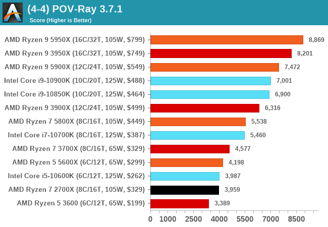
V-Ray: Link
We have a couple of renderers and ray tracers in our suite already, however V-Ray’s benchmark came through for a requested benchmark enough for us to roll it into our suite. Built by ChaosGroup, V-Ray is a 3D rendering package compatible with a number of popular commercial imaging applications, such as 3ds Max, Maya, Undreal, Cinema 4D, and Blender.
We run the standard standalone benchmark application, but in an automated fashion to pull out the result in the form of kilosamples/second. We run the test six times and take an average of the valid results.
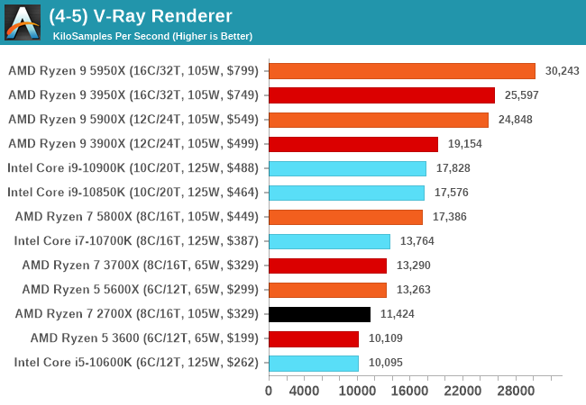
Cinebench R20: Link
Another common stable of a benchmark suite is Cinebench. Based on Cinema4D, Cinebench is a purpose built benchmark machine that renders a scene with both single and multi-threaded options. The scene is identical in both cases. The R20 version means that it targets Cinema 4D R20, a slightly older version of the software which is currently on version R21. Cinebench R20 was launched given that the R15 version had been out a long time, and despite the difference between the benchmark and the latest version of the software on which it is based, Cinebench results are often quoted a lot in marketing materials.
Results for Cinebench R20 are not comparable to R15 or older, because both the scene being used is different, but also the updates in the code path. The results are output as a score from the software, which is directly proportional to the time taken. Using the benchmark flags for single CPU and multi-CPU workloads, we run the software from the command line which opens the test, runs it, and dumps the result into the console which is redirected to a text file. The test is repeated for a minimum of 10 minutes for both ST and MT, and then the runs averaged.
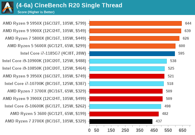
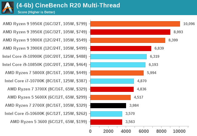
CPU Tests: Encoding
One of the interesting elements on modern processors is encoding performance. This covers two main areas: encryption/decryption for secure data transfer, and video transcoding from one video format to another.
In the encrypt/decrypt scenario, how data is transferred and by what mechanism is pertinent to on-the-fly encryption of sensitive data - a process by which more modern devices are leaning to for software security.
Video transcoding as a tool to adjust the quality, file size and resolution of a video file has boomed in recent years, such as providing the optimum video for devices before consumption, or for game streamers who are wanting to upload the output from their video camera in real-time. As we move into live 3D video, this task will only get more strenuous, and it turns out that the performance of certain algorithms is a function of the input/output of the content.
HandBrake 1.32: Link
Video transcoding (both encode and decode) is a hot topic in performance metrics as more and more content is being created. First consideration is the standard in which the video is encoded, which can be lossless or lossy, trade performance for file-size, trade quality for file-size, or all of the above can increase encoding rates to help accelerate decoding rates. Alongside Google's favorite codecs, VP9 and AV1, there are others that are prominent: H264, the older codec, is practically everywhere and is designed to be optimized for 1080p video, and HEVC (or H.265) that is aimed to provide the same quality as H264 but at a lower file-size (or better quality for the same size). HEVC is important as 4K is streamed over the air, meaning less bits need to be transferred for the same quality content. There are other codecs coming to market designed for specific use cases all the time.
Handbrake is a favored tool for transcoding, with the later versions using copious amounts of newer APIs to take advantage of co-processors, like GPUs. It is available on Windows via an interface or can be accessed through the command-line, with the latter making our testing easier, with a redirection operator for the console output.
We take the compiled version of this 16-minute YouTube video about Russian CPUs at 1080p30 h264 and convert into three different files: (1) 480p30 ‘Discord’, (2) 720p30 ‘YouTube’, and (3) 4K60 HEVC.
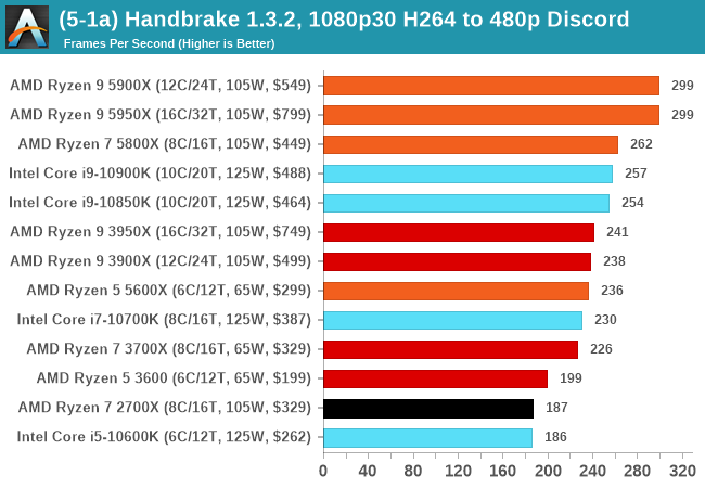
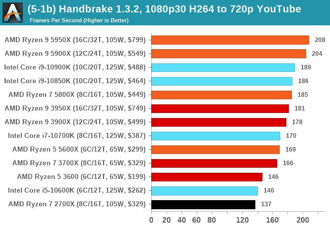
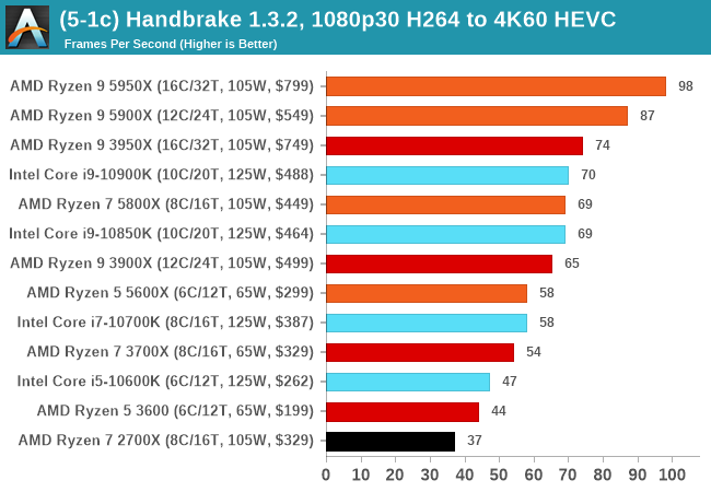
7-Zip 1900: Link
The first compression benchmark tool we use is the open-source 7-zip, which typically offers good scaling across multiple cores. 7-zip is the compression tool most cited by readers as one they would rather see benchmarks on, and the program includes a built-in benchmark tool for both compression and decompression.
The tool can either be run from inside the software or through the command line. We take the latter route as it is easier to automate, obtain results, and put through our process. The command line flags available offer an option for repeated runs, and the output provides the average automatically through the console. We direct this output into a text file and regex the required values for compression, decompression, and a combined score.
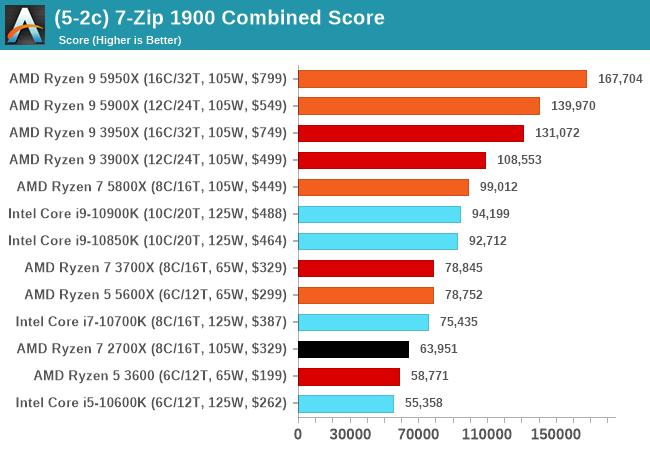
AES Encoding
Algorithms using AES coding have spread far and wide as a ubiquitous tool for encryption. Again, this is another CPU limited test, and modern CPUs have special AES pathways to accelerate their performance. We often see scaling in both frequency and cores with this benchmark. We use the latest version of TrueCrypt and run its benchmark mode over 1GB of in-DRAM data. Results shown are the GB/s average of encryption and decryption.
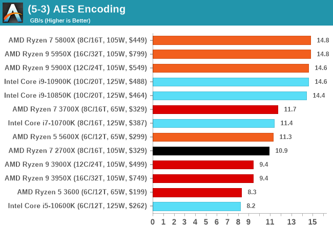
WinRAR 5.90: Link
For the 2020 test suite, we move to the latest version of WinRAR in our compression test. WinRAR in some quarters is more user friendly that 7-Zip, hence its inclusion. Rather than use a benchmark mode as we did with 7-Zip, here we take a set of files representative of a generic stack
- 33 video files , each 30 seconds, in 1.37 GB,
- 2834 smaller website files in 370 folders in 150 MB,
- 100 Beat Saber music tracks and input files, for 451 MB
This is a mixture of compressible and incompressible formats. The results shown are the time taken to encode the file. Due to DRAM caching, we run the test for 20 minutes times and take the average of the last five runs when the benchmark is in a steady state.
For automation, we use AHK’s internal timing tools from initiating the workload until the window closes signifying the end. This means the results are contained within AHK, with an average of the last 5 results being easy enough to calculate.
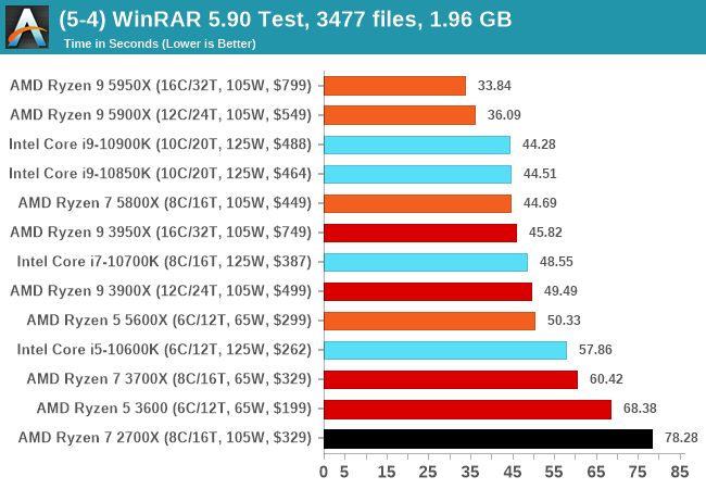
CPU Tests: Legacy and Web
In order to gather data to compare with older benchmarks, we are still keeping a number of tests under our ‘legacy’ section. This includes all the former major versions of CineBench (R15, R11.5, R10) as well as x264 HD 3.0 and the first very naïve version of 3DPM v2.1. We won’t be transferring the data over from the old testing into Bench, otherwise it would be populated with 200 CPUs with only one data point, so it will fill up as we test more CPUs like the others.
The other section here is our web tests.
Web Tests: Kraken, Octane, and Speedometer
Benchmarking using web tools is always a bit difficult. Browsers change almost daily, and the way the web is used changes even quicker. While there is some scope for advanced computational based benchmarks, most users care about responsiveness, which requires a strong back-end to work quickly to provide on the front-end. The benchmarks we chose for our web tests are essentially industry standards – at least once upon a time.
It should be noted that for each test, the browser is closed and re-opened a new with a fresh cache. We use a fixed Chromium version for our tests with the update capabilities removed to ensure consistency.
Mozilla Kraken 1.1
Kraken is a 2010 benchmark from Mozilla and does a series of JavaScript tests. These tests are a little more involved than previous tests, looking at artificial intelligence, audio manipulation, image manipulation, json parsing, and cryptographic functions. The benchmark starts with an initial download of data for the audio and imaging, and then runs through 10 times giving a timed result.
We loop through the 10-run test four times (so that’s a total of 40 runs), and average the four end-results. The result is given as time to complete the test, and we’re reaching a slow asymptotic limit with regards the highest IPC processors.
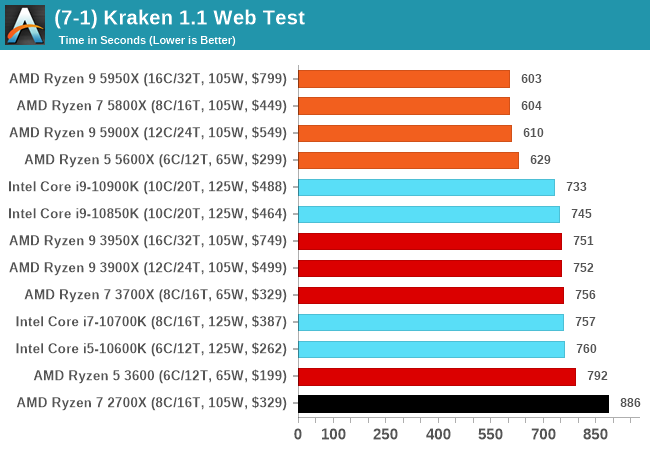
Google Octane 2.0
Our second test is also JavaScript based, but uses a lot more variation of newer JS techniques, such as object-oriented programming, kernel simulation, object creation/destruction, garbage collection, array manipulations, compiler latency and code execution.
Octane was developed after the discontinuation of other tests, with the goal of being more web-like than previous tests. It has been a popular benchmark, making it an obvious target for optimizations in the JavaScript engines. Ultimately it was retired in early 2017 due to this, although it is still widely used as a tool to determine general CPU performance in a number of web tasks.
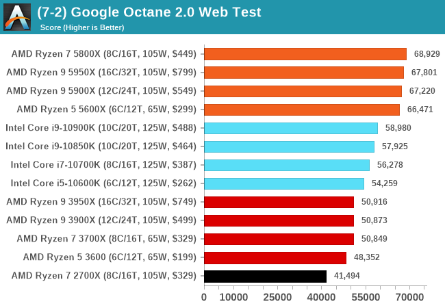
Speedometer 2: JavaScript Frameworks
Our newest web test is Speedometer 2, which is a test over a series of JavaScript frameworks to do three simple things: built a list, enable each item in the list, and remove the list. All the frameworks implement the same visual cues, but obviously apply them from different coding angles.
Our test goes through the list of frameworks, and produces a final score indicative of ‘rpm’, one of the benchmarks internal metrics.
We repeat over the benchmark for a dozen loops, taking the average of the last five.
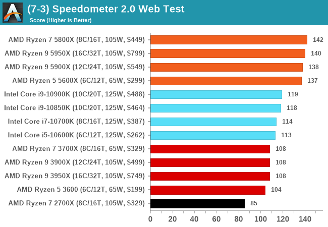
Legacy Tests
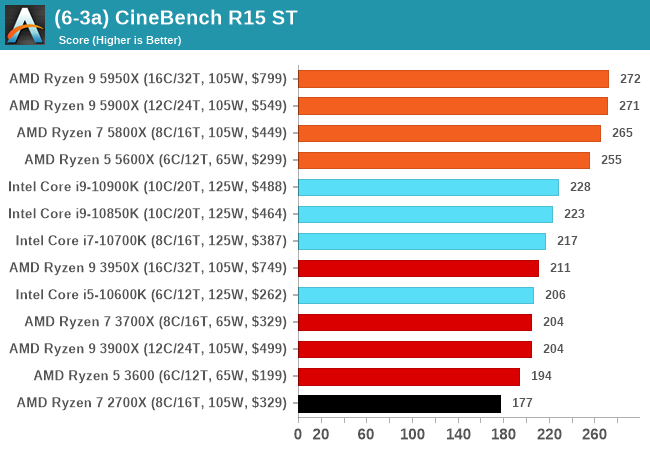
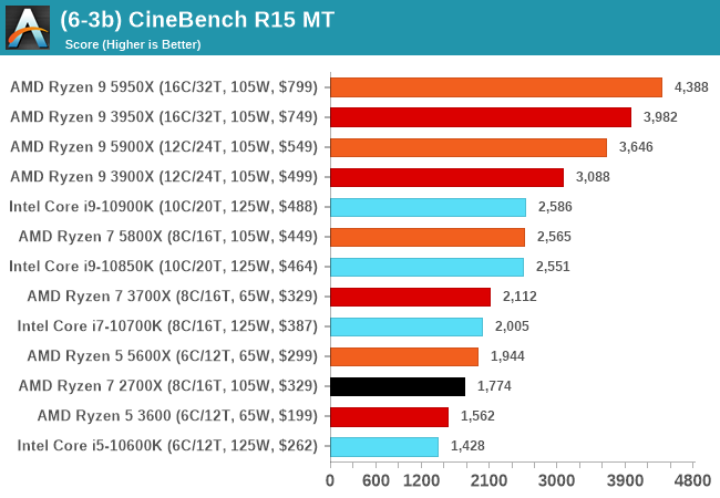
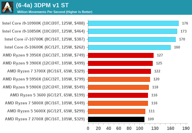
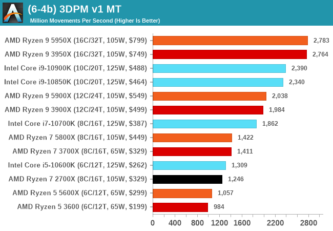
CPU Tests: Synthetic
Most of the people in our industry have a love/hate relationship when it comes to synthetic tests. On the one hand, they’re often good for quick summaries of performance and are easy to use, but most of the time the tests aren’t related to any real software. Synthetic tests are often very good at burrowing down to a specific set of instructions and maximizing the performance out of those. Due to requests from a number of our readers, we have the following synthetic tests.
Linux OpenSSL Speed: SHA256
One of our readers reached out in early 2020 and stated that he was interested in looking at OpenSSL hashing rates in Linux. Luckily OpenSSL in Linux has a function called ‘speed’ that allows the user to determine how fast the system is for any given hashing algorithm, as well as signing and verifying messages.
OpenSSL offers a lot of algorithms to choose from, and based on a quick Twitter poll, we narrowed it down to the following:
- rsa2048 sign and rsa2048 verify
- sha256 at 8K block size
- md5 at 8K block size
For each of these tests, we run them in single thread and multithreaded mode. All the graphs are in our benchmark database, Bench, and we use the sha256 and md5 results in published reviews.
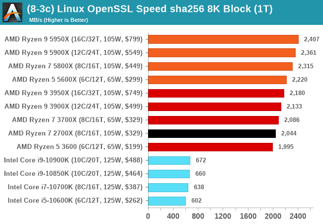
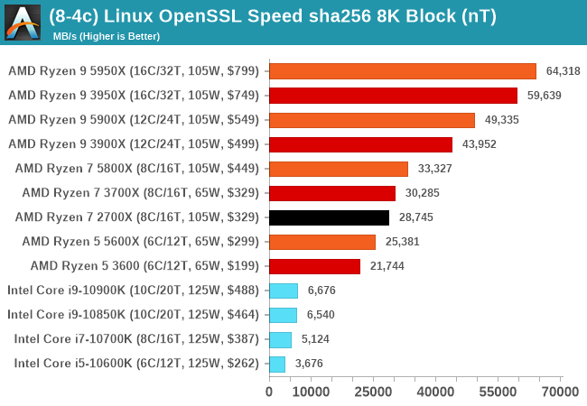
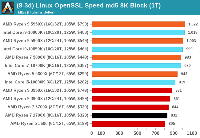
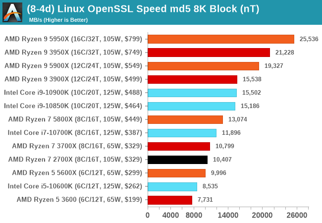
GeekBench 5: Link
As a common tool for cross-platform testing between mobile, PC, and Mac, GeekBench is an ultimate exercise in synthetic testing across a range of algorithms looking for peak throughput. Tests include encryption, compression, fast Fourier transform, memory operations, n-body physics, matrix operations, histogram manipulation, and HTML parsing.
I’m including this test due to popular demand, although the results do come across as overly synthetic, and a lot of users often put a lot of weight behind the test due to the fact that it is compiled across different platforms (although with different compilers).
We have both GB5 and GB4 results in our benchmark database. GB5 was introduced to our test suite after already having tested ~25 CPUs, and so the results are a little sporadic by comparison. These spots will be filled in when we retest any of the CPUs.
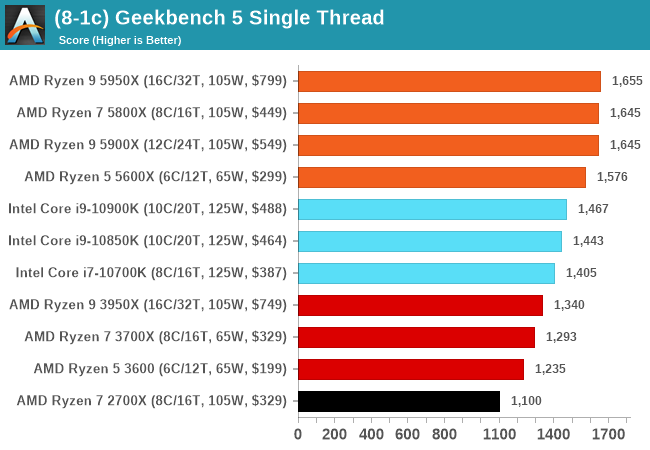
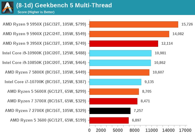
Gaming Tests: Chernobylite
Despite the advent of recent TV shows like Chernobyl, recreating the situation revolving around the 1986 Chernobyl nuclear disaster, the concept of nuclear fallout and the town of Pripyat have been popular settings for a number of games – mostly first person shooters. Chernobylite is an indie title that plays on a science-fiction survival horror experience and uses a 3D-scanned recreation of the real Chernobyl Exclusion Zone. It involves challenging combat, a mix of free exploration with crafting and non-linear story telling. While still in early access, it is already picking up plenty of awards.
I picked up Chernobylite while still in early access, and was impressed by its in-game benchmark, showcasing complex building structure with plenty of trees and structures where aliasing becomes important. The in-game benchmark is an on-rails experience through the scenery, covering both indoor and outdoor scenes – it ends up being very CPU limited in the way it is designed. We have taken an offline version of Chernobylite to use in our tests, and we are testing the following settings combinations:
- 360p Low, 1440p Low, 4K Low, 1080p Max
We do as many runs within 10 minutes per resolution/setting combination, and then take averages.
| AnandTech | Low Resolution Low Quality |
Medium Resolution Low Quality |
High Resolution Low Quality |
Medium Resolution Max Quality |
| Average FPS |  |
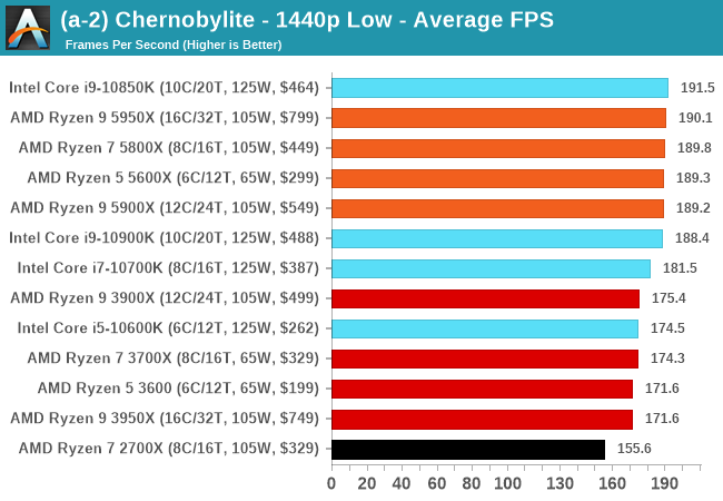 |
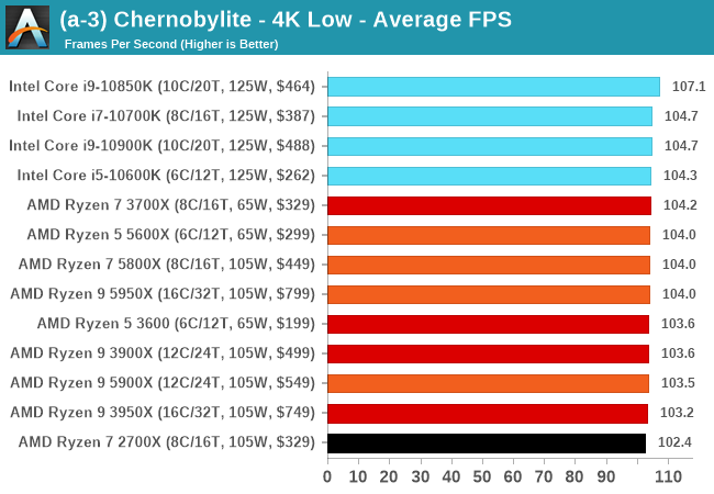 |
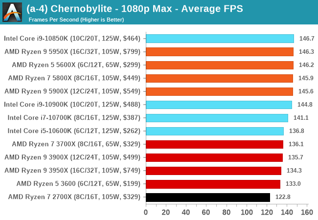 |
All of our benchmark results can also be found in our benchmark engine, Bench.
Gaming Tests: Civilization 6
Originally penned by Sid Meier and his team, the Civilization series of turn-based strategy games are a cult classic, and many an excuse for an all-nighter trying to get Gandhi to declare war on you due to an integer underflow. Truth be told I never actually played the first version, but I have played every edition from the second to the sixth, including the fourth as voiced by the late Leonard Nimoy, and it a game that is easy to pick up, but hard to master.
Benchmarking Civilization has always been somewhat of an oxymoron – for a turn based strategy game, the frame rate is not necessarily the important thing here and even in the right mood, something as low as 5 frames per second can be enough. With Civilization 6 however, Firaxis went hardcore on visual fidelity, trying to pull you into the game. As a result, Civilization can taxing on graphics and CPUs as we crank up the details, especially in DirectX 12.
For this benchmark, we are using the following settings:
- 480p Low, 1440p Low, 4K Low, 1080p Max
For automation, Firaxis supports the in-game automated benchmark from the command line, and output a results file with frame times. We do as many runs within 10 minutes per resolution/setting combination, and then take averages and percentiles.
| AnandTech | Low Resolution Low Quality |
Medium Resolution Low Quality |
High Resolution Low Quality |
Medium Resolution Max Quality |
| Average FPS |  |
 |
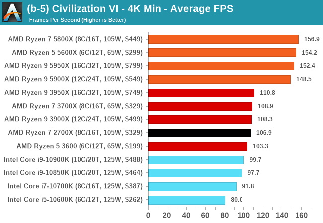 |
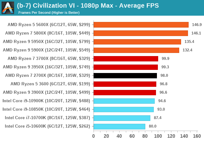 |
| 95th Percentile | 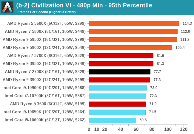 |
 |
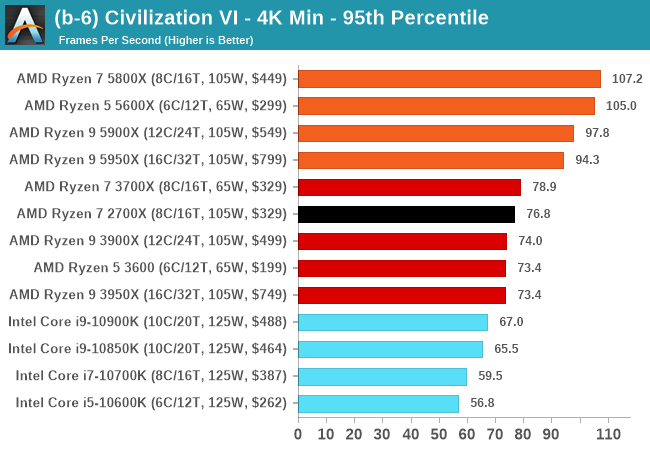 |
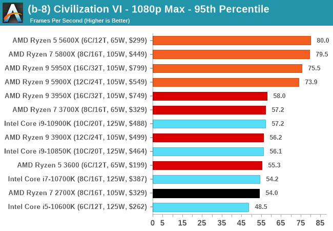 |
All of our benchmark results can also be found in our benchmark engine, Bench.
Gaming Tests: Deus Ex Mankind Divided
Deus Ex is a franchise with a wide level of popularity. Despite the Deus Ex: Mankind Divided (DEMD) version being released in 2016, it has often been heralded as a game that taxes the CPU. It uses the Dawn Engine to create a very complex first-person action game with science-fiction based weapons and interfaces. The game combines first-person, stealth, and role-playing elements, with the game set in Prague, dealing with themes of transhumanism, conspiracy theories, and a cyberpunk future. The game allows the player to select their own path (stealth, gun-toting maniac) and offers multiple solutions to its puzzles.
DEMD has an in-game benchmark, an on-rails look around an environment showcasing some of the game’s most stunning effects, such as lighting, texturing, and others. Even in 2020, it’s still an impressive graphical showcase when everything is jumped up to the max. For this title, we are testing the following resolutions:
- 600p Low, 1440p Low, 4K Low, 1080p Max
The benchmark runs for about 90 seconds. We do as many runs within 10 minutes per resolution/setting combination, and then take averages and percentiles.
| AnandTech | Low Resolution Low Quality |
Medium Resolution Low Quality |
High Resolution Low Quality |
Medium Resolution Max Quality |
| Average FPS |  |
 |
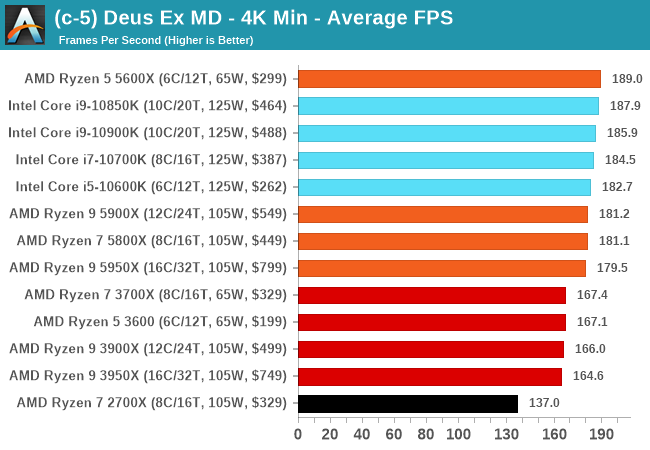 |
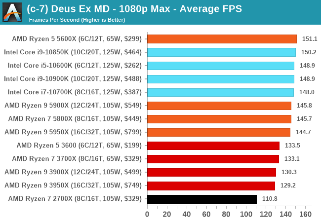 |
| 95th Percentile |  |
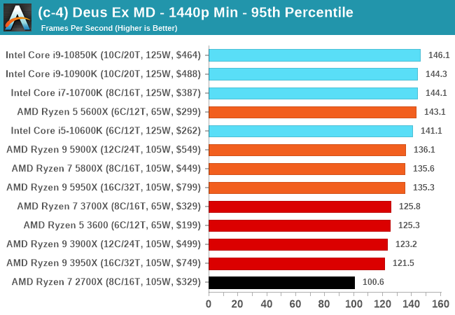 |
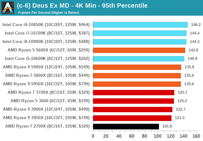 |
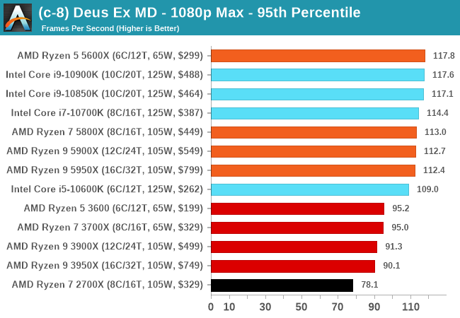 |
All of our benchmark results can also be found in our benchmark engine, Bench.
Gaming Tests: Final Fantasy XIV
Despite being one number less than Final Fantasy 15, because FF14 is a massively-multiplayer online title, there are always yearly update packages which give the opportunity for graphical updates too. In 2019, FFXIV launched its Shadowbringers expansion, and an official standalone benchmark was released at the same time for users to understand what level of performance they could expect. Much like the FF15 benchmark we’ve been using for a while, this test is a long 7-minute scene of simulated gameplay within the title. There are a number of interesting graphical features, and it certainly looks more like a 2019 title than a 2010 release, which is when FF14 first came out.
With this being a standalone benchmark, we do not have to worry about updates, and the idea for these sort of tests for end-users is to keep the code base consistent. For our testing suite, we are using the following settings:
- 768p Minimum, 1440p Minimum, 4K Minimum, 1080p Maximum
As with the other benchmarks, we do as many runs until 10 minutes per resolution/setting combination has passed, and then take averages. Realistically, because of the length of this test, this equates to two runs per setting.
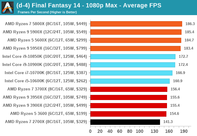
| AnandTech | Low Resolution Low Quality |
Medium Resolution Low Quality |
High Resolution Low Quality |
Medium Resolution Max Quality |
| Average FPS | 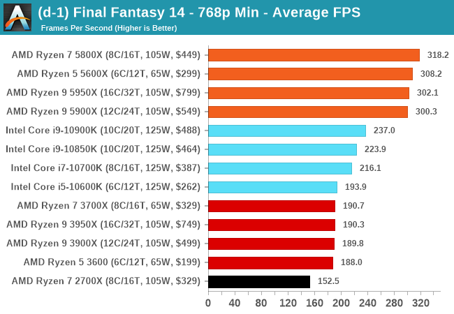 |
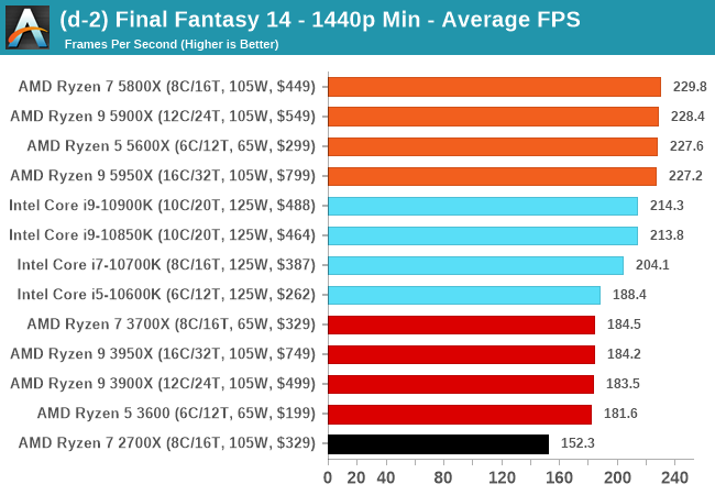 |
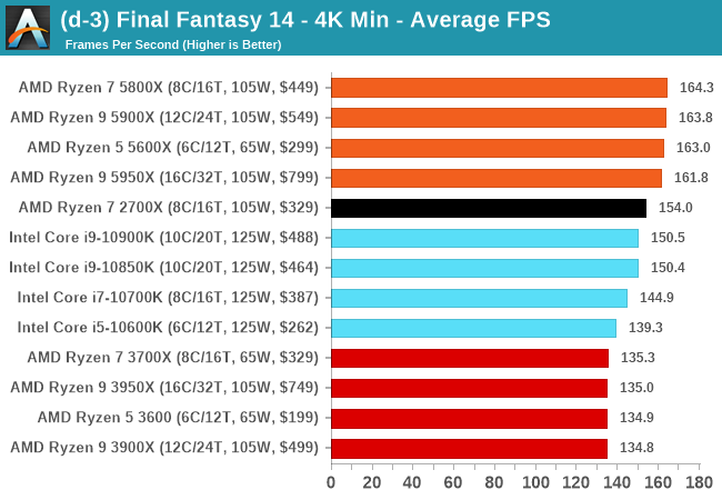 |
 |
All of our benchmark results can also be found in our benchmark engine, Bench.
Gaming Tests: Final Fantasy XV
Upon arriving to PC, Final Fantasy XV: Windows Edition was given a graphical overhaul as it was ported over from console. As a fantasy RPG with a long history, the fruits of Square-Enix’s successful partnership with NVIDIA are on display. The game uses the internal Luminous Engine, and as with other Final Fantasy games, pushes the imagination of what we can do with the hardware underneath us. To that end, FFXV was one of the first games to promote the use of ‘video game landscape photography’, due in part to the extensive detail even at long range but also with the integration of NVIDIA’s Ansel software, that allowed for super-resolution imagery and post-processing effects to be applied.
In preparation for the launch of the game, Square Enix opted to release a standalone benchmark. Using the Final Fantasy XV standalone benchmark gives us a lengthy standardized sequence to record, although it should be noted that its heavy use of NVIDIA technology means that the Maximum setting has problems - it renders items off screen. To get around this, we use the standard preset which does not have these issues. We use the following settings:
- 720p Standard, 1080p Standard, 4K Standard, 8K Standard
For automation, the title accepts command line inputs for both resolution and settings, and then auto-quits when finished. As with the other benchmarks, we do as many runs until 10 minutes per resolution/setting combination has passed, and then take averages. Realistically, because of the length of this test, this equates to two runs per setting.
| AnandTech | Low Resolution Low Quality |
Medium Resolution Low Quality |
High Resolution Low Quality |
Medium Resolution Max Quality |
| Average FPS |  |
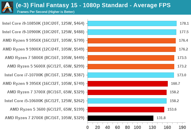 |
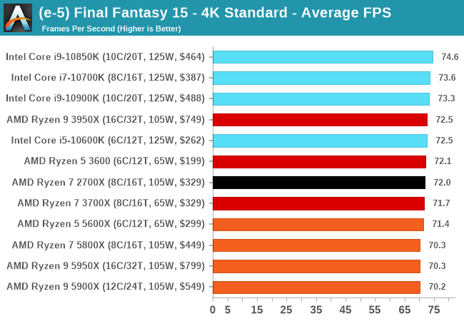 |
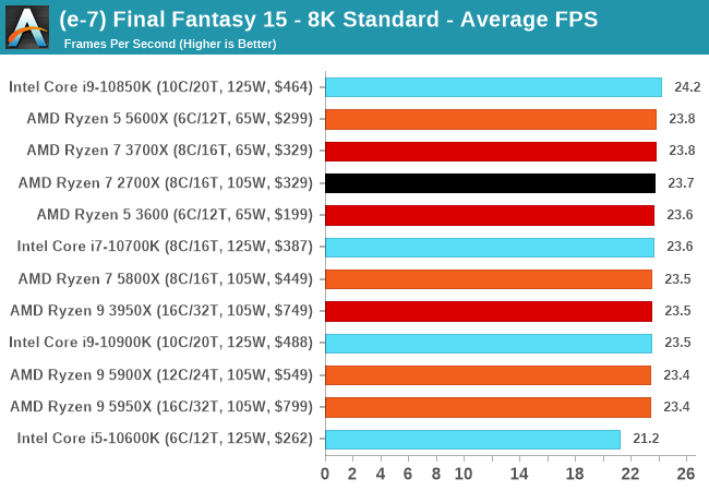 |
| 95th Percentile | 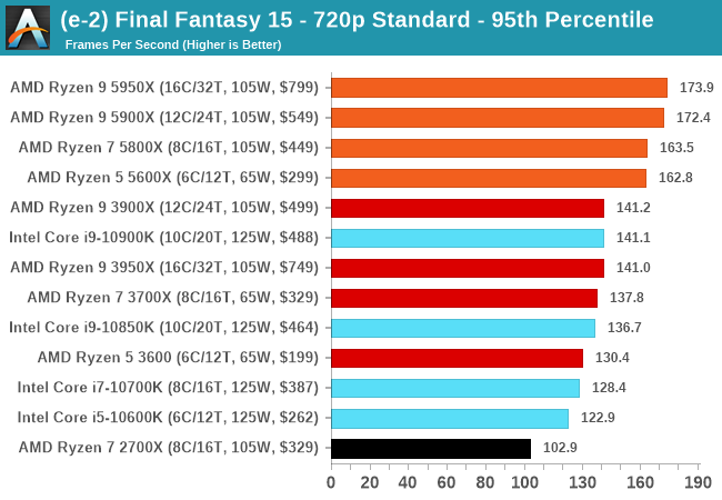 |
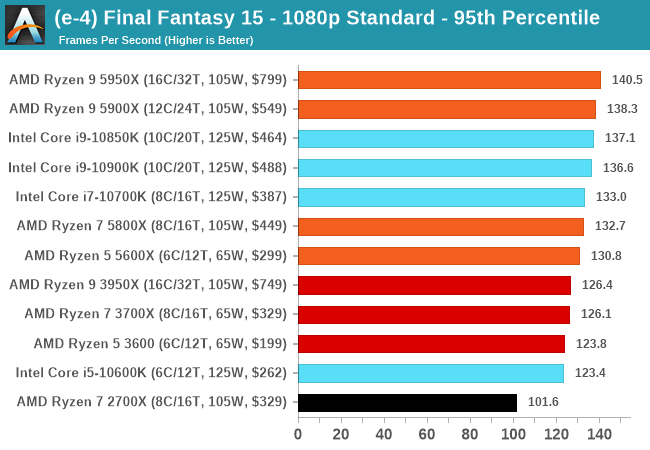 |
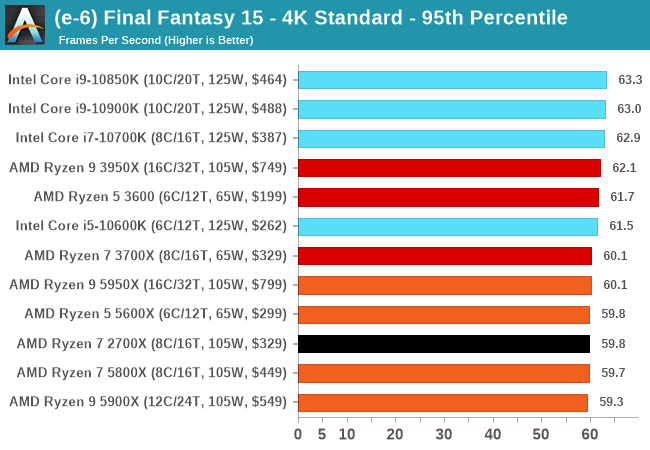 |
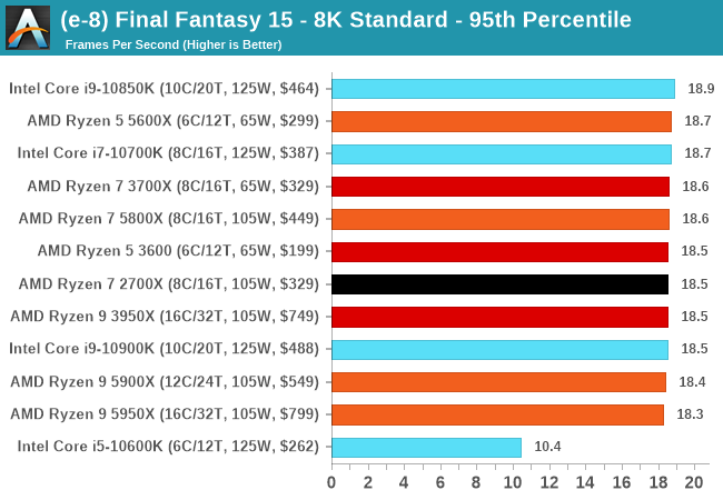 |
All of our benchmark results can also be found in our benchmark engine, Bench.
Gaming Tests: World of Tanks
Albeit different to most of the other commonly played MMO or massively multiplayer online games, World of Tanks is set in the mid-20th century and allows players to take control of a range of military based armored vehicles. World of Tanks (WoT) is developed and published by Wargaming who are based in Belarus, with the game’s soundtrack being primarily composed by Belarusian composer Sergey Khmelevsky. The game offers multiple entry points including a free-to-play element as well as allowing players to pay a fee to open up more features. One of the most interesting things about this tank based MMO is that it achieved eSports status when it debuted at the World Cyber Games back in 2012.
World of Tanks enCore is a demo application for its new graphics engine penned by the Wargaming development team. Over time the new core engine has been implemented into the full game upgrading the games visuals with key elements such as improved water, flora, shadows, lighting as well as other objects such as buildings. The World of Tanks enCore demo app not only offers up insight into the impending game engine changes, but allows users to check system performance to see if the new engine runs optimally on their system. There is technically a Ray Tracing version of the enCore benchmark now available, however because it can’t be deployed standalone without the installer, we decided against using it. If that gets fixed, then we can look into it.
The benchmark tool comes with a number of presets:
- 768p Minimum, 1080p Standard, 1080p Max, 4K Max (not a preset)
The odd one out is the 4K Max preset, because the benchmark doesn’t automatically have a 4K option – to get this we edit the acceptable resolutions ini file, and then we can select 4K. The benchmark outputs its own results file, with frame times, making it very easy to parse the data needed for average and percentiles.
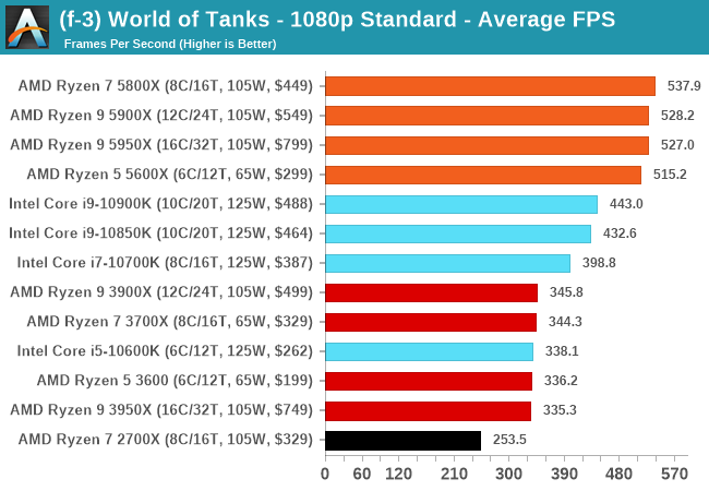
| AnandTech | Low Resolution Low Quality |
Medium Resolution Low Quality |
High Resolution Low Quality |
Medium Resolution Max Quality |
| Average FPS | 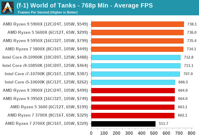 |
 |
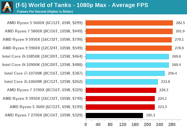 |
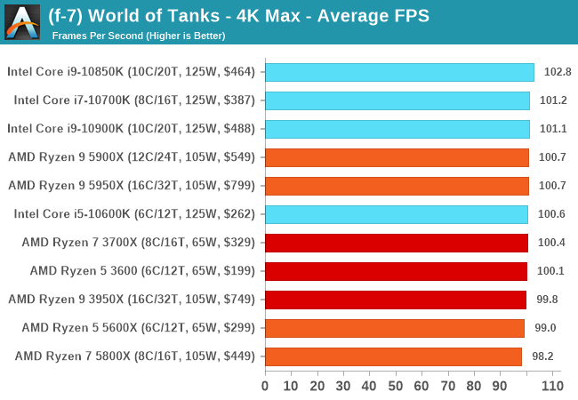 |
| 95th Percentile | 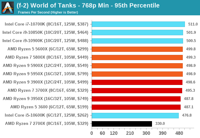 |
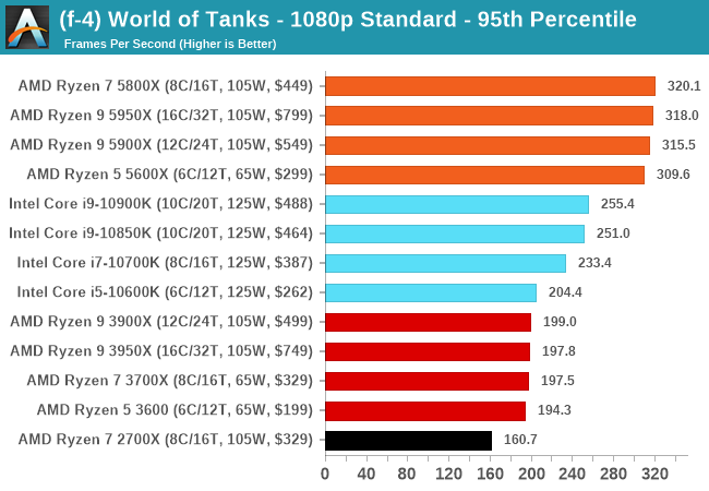 |
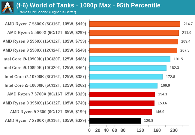 |
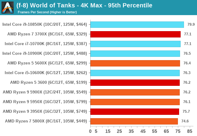 |
All of our benchmark results can also be found in our benchmark engine, Bench.
Gaming Tests: Borderlands 3
As a big Borderlands fan, having to sit and wait six months for the EPIC Store exclusive to expire before we saw it on Steam felt like a long time to wait. The fourth title of the franchise, if you exclude the TellTale style-games, BL3 expands the universe beyond Pandora and its orbit, with the set of heroes (plus those from previous games) now cruising the galaxy looking for vaults and the treasures within. Popular Characters like Tiny Tina, Claptrap, Lilith, Dr. Zed, Zer0, Tannis, and others all make appearances as the game continues its cel-shaded design but with the graphical fidelity turned up. Borderlands 1 gave me my first ever taste of proper in-game second order PhysX, and it’s a high standard that continues to this day.
BL3 works best with online access, so it is filed under our online games section. BL3 is also one of our biggest downloads, requiring 100+ GB. As BL3 supports resolution scaling, we are using the following settings:
- 360p Very Low, 1440p Very Low, 4K Very Low, 1080p Badass
BL3 has its own in-game benchmark, which recreates a set of on-rails scenes with a variety of activity going on in each, such as shootouts, explosions, and wildlife. The benchmark outputs its own results files, including frame times, which can be parsed for our averages/percentile data.
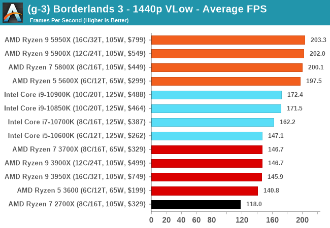
| AnandTech | Low Resolution Low Quality |
Medium Resolution Low Quality |
High Resolution Low Quality |
Medium Resolution Max Quality |
| Average FPS | 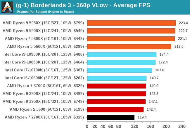 |
 |
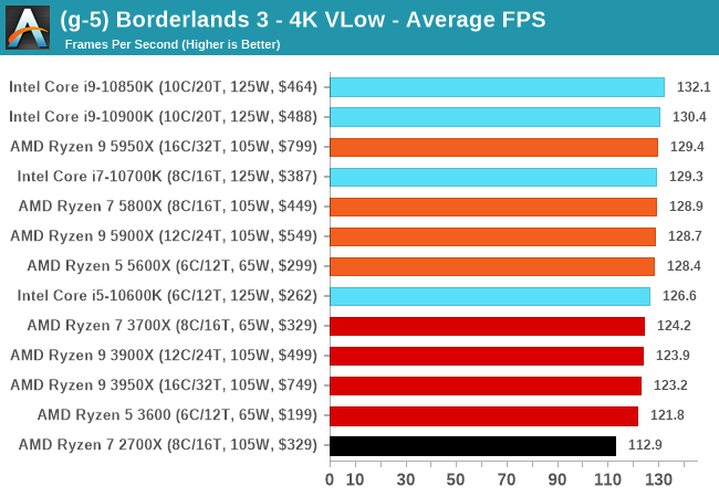 |
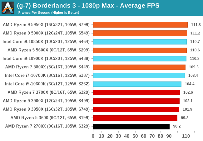 |
| 95th Percentile |  |
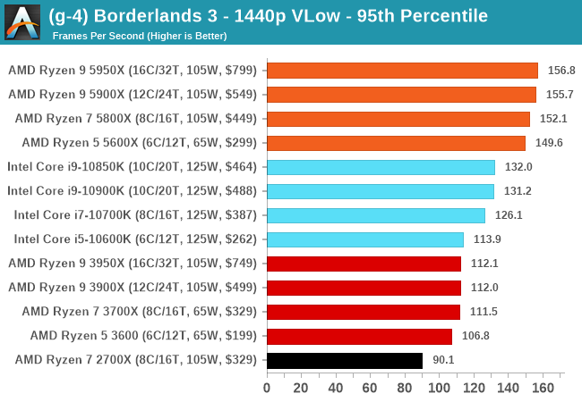 |
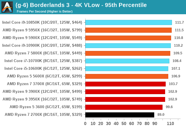 |
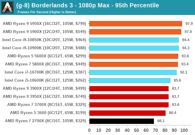 |
All of our benchmark results can also be found in our benchmark engine, Bench.
Gaming Tests: F1 2019
The F1 racing games from Codemasters have been popular benchmarks in the tech community, mostly for ease-of-use and that they seem to take advantage of any area of a machine that might be better than another. The 2019 edition of the game features all 21 circuits on the calendar for that year, and includes a range of retro models and DLC focusing on the careers of Alain Prost and Ayrton Senna. Built on the EGO Engine 3.0, the game has been criticized similarly to most annual sports games, by not offering enough season-to-season graphical fidelity updates to make investing in the latest title worth it, however the 2019 edition revamps up the Career mode, with features such as in-season driver swaps coming into the mix. The quality of the graphics this time around is also superb, even at 4K low or 1080p Ultra.
For our test, we put Alex Albon in the Red Bull in position #20, for a dry two-lap race around Austin. We test at the following settings:
- 768p Ultra Low, 1440p Ultra Low, 4K Ultra Low, 1080p Ultra
In terms of automation, F1 2019 has an in-game benchmark that can be called from the command line, and the output file has frame times. We repeat each resolution setting for a minimum of 10 minutes, taking the averages and percentiles.
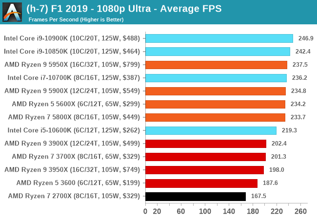
| AnandTech | Low Resolution Low Quality |
Medium Resolution Low Quality |
High Resolution Low Quality |
Medium Resolution Max Quality |
| Average FPS | 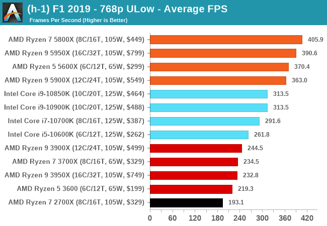 |
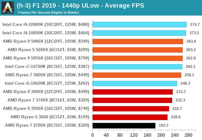 |
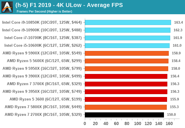 |
 |
| 95th Percentile | 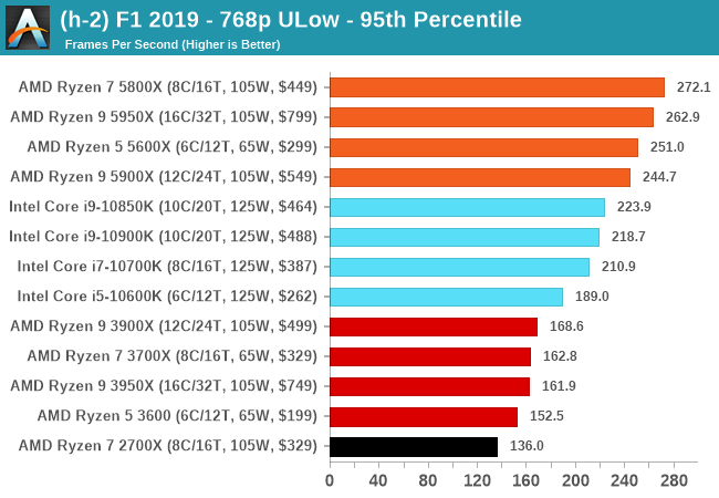 |
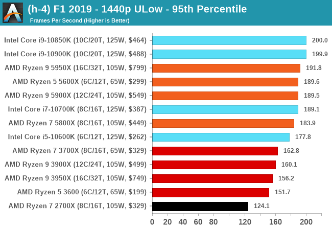 |
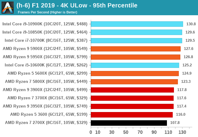 |
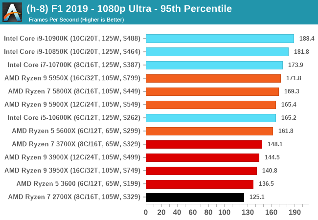 |
All of our benchmark results can also be found in our benchmark engine, Bench.
Gaming Tests: Far Cry 5
The fifth title in Ubisoft's Far Cry series lands us right into the unwelcoming arms of an armed militant cult in Montana, one of the many middles-of-nowhere in the United States. With a charismatic and enigmatic adversary, gorgeous landscapes of the northwestern American flavor, and lots of violence, it is classic Far Cry fare. Graphically intensive in an open-world environment, the game mixes in action and exploration with a lot of configurability.
Unfortunately, the game doesn’t like us changing the resolution in the results file when using certain monitors, resorting to 1080p but keeping the quality settings. But resolution scaling does work, so we decided to fix the resolution at 1080p and use a variety of different scaling factors to give the following:
- 720p Low, 1440p Low, 4K Low, 1440p Max.
Far Cry 5 outputs a results file here, but that the file is a HTML file, which showcases a graph of the FPS detected. At no point in the HTML file does it contain the frame times for each frame, but it does show the frames per second, as a value once per second in the graph. The graph in HTML form is a series of (x,y) co-ordinates scaled to the min/max of the graph, rather than the raw (second, FPS) data, and so using regex I carefully tease out the values of the graph, convert them into a (second, FPS) format, and take our values of averages and percentiles that way.
If anyone from Ubisoft wants to chat about building a benchmark platform that would not only help me but also every other member of the tech press build our benchmark testing platform to help our readers decide what is the best hardware to use on your games, please reach out to [email protected]. Some of the suggestions I want to give you will take less than half a day and it’s easily free advertising to use the benchmark over the next couple of years (or more).
As with the other gaming tests, we run each resolution/setting combination for a minimum of 10 minutes and take the relevant frame data for averages and percentiles.
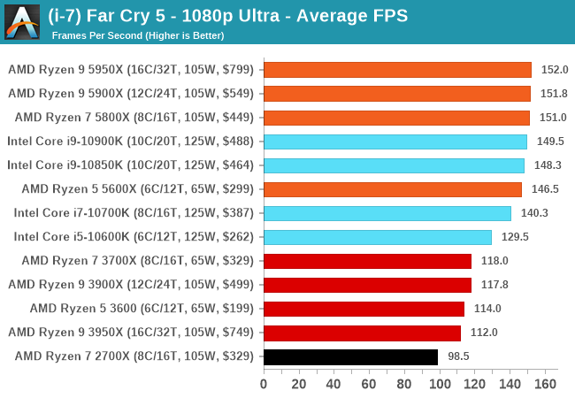
| AnandTech | Low Resolution Low Quality |
Medium Resolution Low Quality |
High Resolution Low Quality |
Medium Resolution Max Quality |
| Average FPS | 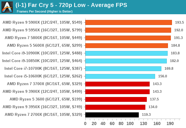 |
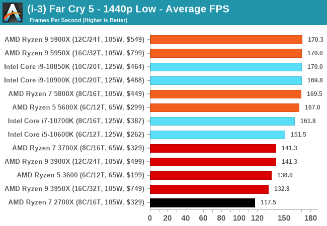 |
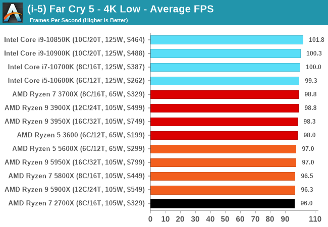 |
 |
| 95th Percentile | 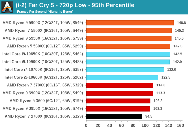 |
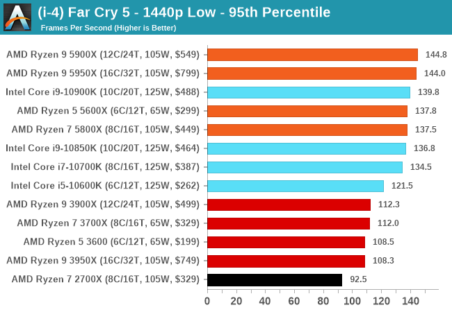 |
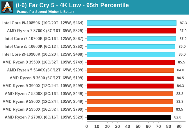 |
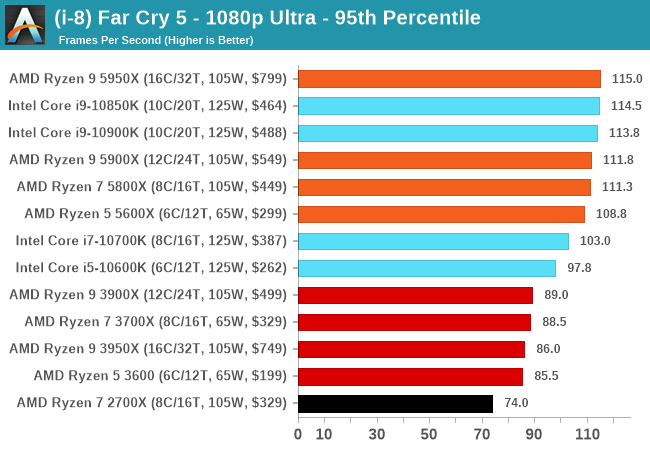 |
All of our benchmark results can also be found in our benchmark engine, Bench.
Gaming Tests: Gears Tactics
Remembering the original Gears of War brings back a number of memories – some good, and some involving online gameplay. The latest iteration of the franchise was launched as I was putting this benchmark suite together, and Gears Tactics is a high-fidelity turn-based strategy game with an extensive single player mode. As with a lot of turn-based games, there is ample opportunity to crank up the visual effects, and here the developers have put a lot of effort into creating effects, a number of which seem to be CPU limited.
Gears Tactics has an in-game benchmark, roughly 2.5 minutes of AI gameplay starting from the same position but using a random seed for actions. Much like the racing games, this usually leads to some variation in the run-to-run data, so for this benchmark we are taking the geometric mean of the results. One of the biggest things that Gears Tactics can do is on the resolution scaling, supporting 8K, and so we are testing the following settings:
- 720p Low, 4K Low, 8K Low, 1080p Ultra
For results, the game showcases a mountain of data when the benchmark is finished, such as how much the benchmark was CPU limited and where, however none of that is ever exported into a file we can use. It’s just a screenshot which we have to read manually.
If anyone from the Gears Tactics team wants to chat about building a benchmark platform that would not only help me but also every other member of the tech press build our benchmark testing platform to help our readers decide what is the best hardware to use on your games, please reach out to [email protected]. Some of the suggestions I want to give you will take less than half a day and it’s easily free advertising to use the benchmark over the next couple of years (or more).
As with the other benchmarks, we do as many runs until 10 minutes per resolution/setting combination has passed. For this benchmark, we manually read each of the screenshots for each quality/setting/run combination. The benchmark does also give 95th percentiles and frame averages, so we can use both of these data points.
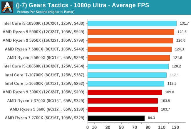
| AnandTech | Low Resolution Low Quality |
Medium Resolution Low Quality |
High Resolution Low Quality |
Medium Resolution Max Quality |
| Average FPS | 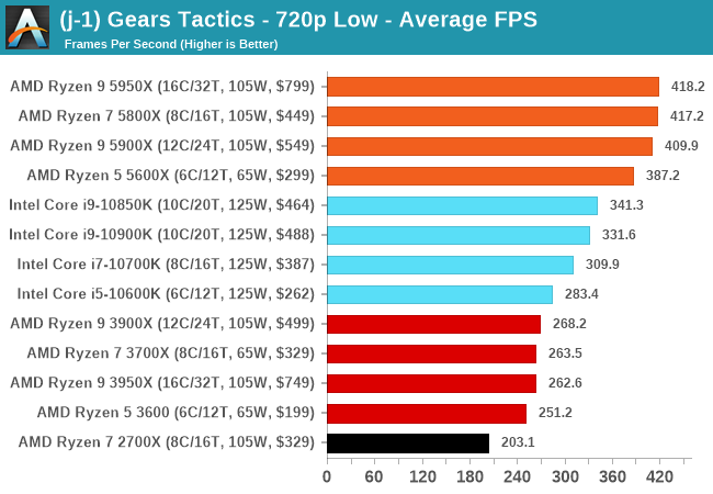 |
 |
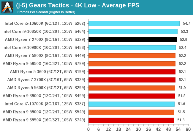 |
 |
| 95th Percentile | 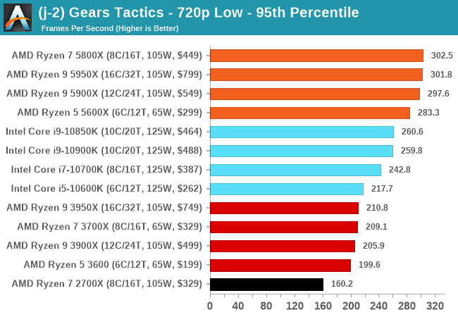 |
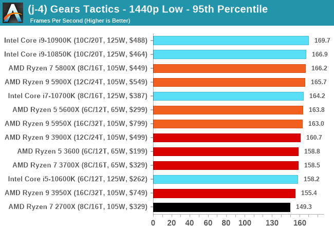 |
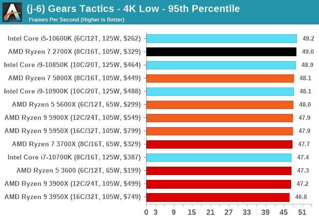 |
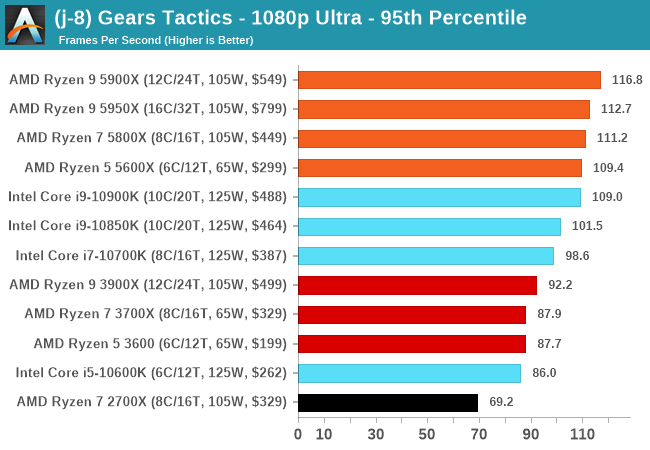 |
All of our benchmark results can also be found in our benchmark engine, Bench.
Gaming Tests: GTA 5
The highly anticipated iteration of the Grand Theft Auto franchise hit the shelves on April 14th 2015, with both AMD and NVIDIA to help optimize the title. At this point GTA V is super old, but still super useful as a benchmark – it is a complicated test with many features that modern titles today still struggle with. With rumors of a GTA 6 on the horizon, I hope Rockstar make that benchmark as easy to use as this one is.
GTA doesn’t provide graphical presets, but opens up the options to users and extends the boundaries by pushing even the hardest systems to the limit using Rockstar’s Advanced Game Engine under DirectX 11. Whether the user is flying high in the mountains with long draw distances or dealing with assorted trash in the city, when cranked up to maximum it creates stunning visuals but hard work for both the CPU and the GPU.
We are using the following settings:
- 720p Low, 1440p Low, 4K Low, 1080p Max
The in-game benchmark consists of five scenarios: four short panning shots with varying lighting and weather effects, and a fifth action sequence that lasts around 90 seconds. We use only the final part of the benchmark, which combines a flight scene in a jet followed by an inner city drive-by through several intersections followed by ramming a tanker that explodes, causing other cars to explode as well. This is a mix of distance rendering followed by a detailed near-rendering action sequence, and the title thankfully spits out frame time data. The benchmark can also be called from the command line, making it very easy to use.
There is one funny caveat with GTA. If the CPU is too slow, or has too few cores, the benchmark loads, but it doesn’t have enough time to put items in the correct position. As a result, for example when running our single core Sandy Bridge system, the jet ends up stuck at the middle of an intersection causing a traffic jam. Unfortunately this means the benchmark never ends, but still amusing.
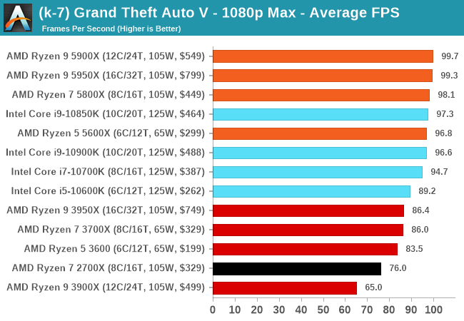
| AnandTech | Low Resolution Low Quality |
Medium Resolution Low Quality |
High Resolution Low Quality |
Medium Resolution Max Quality |
| Average FPS | 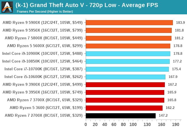 |
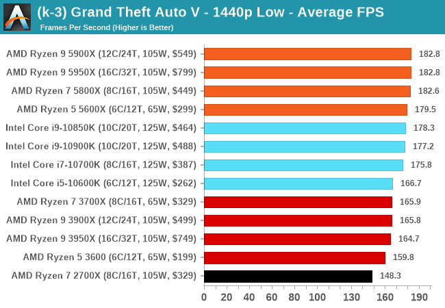 |
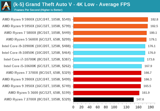 |
 |
| 95th Percentile | 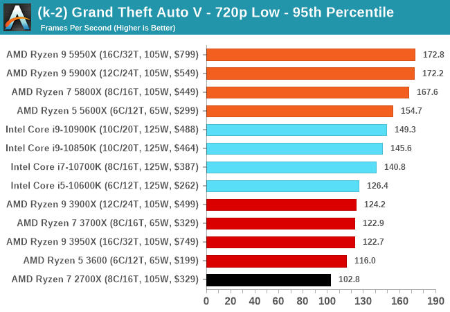 |
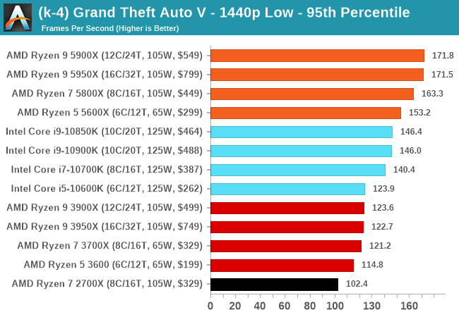 |
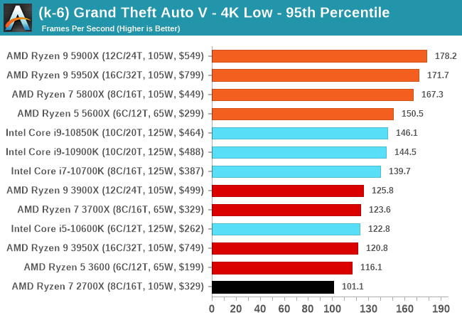 |
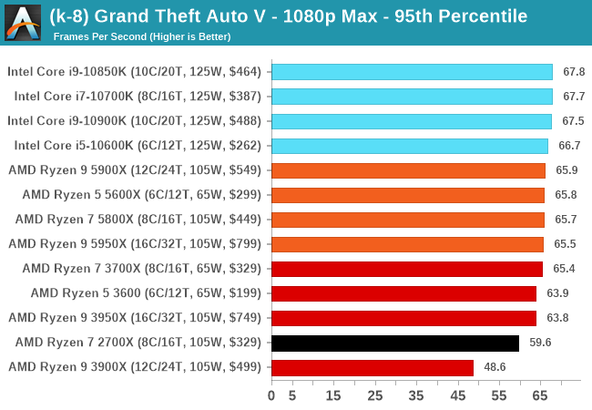 |
All of our benchmark results can also be found in our benchmark engine, Bench.
Gaming Tests: Red Dead Redemption 2
It’s great to have another Rockstar benchmark in the mix, and the launch of Red Dead Redemption 2 (RDR2) on the PC gives us a chance to do that. Building on the success of the original RDR, the second incarnation came to Steam in December 2019 having been released on consoles first. The PC version takes the open-world cowboy genre into the start of the modern age, with a wide array of impressive graphics and features that are eerily close to reality.
For RDR2, Rockstar kept the same benchmark philosophy as with Grand Theft Auto V, with the benchmark consisting of several cut scenes with different weather and lighting effects, with a final scene focusing on an on-rails environment, only this time with mugging a shop leading to a shootout on horseback before riding over a bridge into the great unknown. Luckily most of the command line options from GTA V are present here, and the game also supports resolution scaling. We have the following tests:
- 384p Minimum, 1440p Minimum, 8K Minimum, 1080p Max
For that 8K setting, I originally thought I had the settings file at 4K and 1.0x scaling, but it was actually set at 2.0x giving that 8K. For the sake of it, I decided to keep the 8K settings.
For our results, we run through each resolution and setting configuration for a minimum of 10 minutes, before averaging and parsing the frame time data.
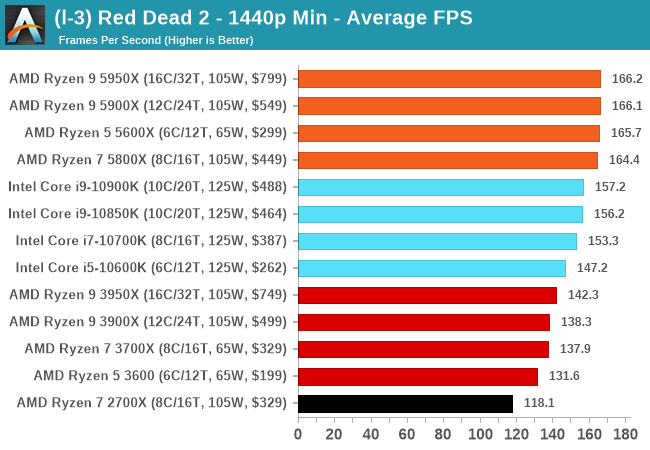
| AnandTech | Low Resolution Low Quality |
Medium Resolution Low Quality |
High Resolution Low Quality |
Medium Resolution Max Quality |
| Average FPS | 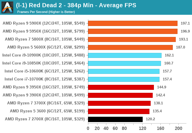 |
 |
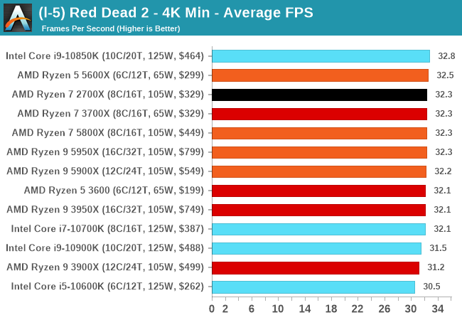 |
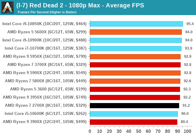 |
| 95th Percentile | 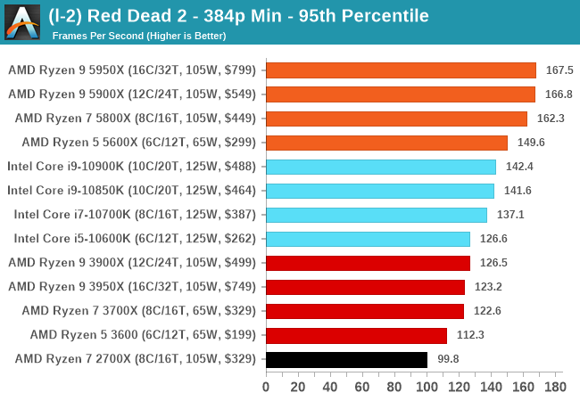 |
 |
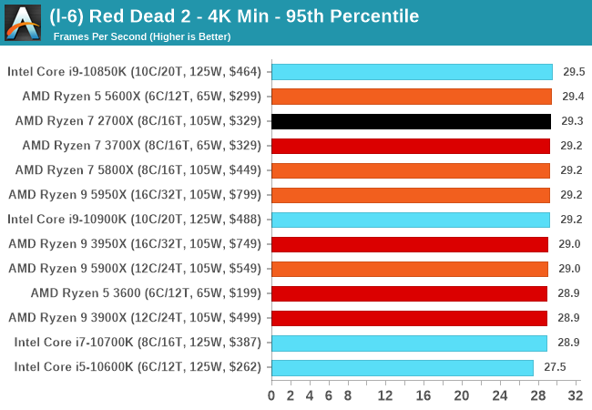 |
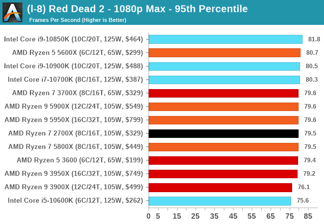 |
All of our benchmark results can also be found in our benchmark engine, Bench.
Gaming Tests: Strange Brigade
Strange Brigade is based in 1903’s Egypt, and follows a story which is very similar to that of the Mummy film franchise. This particular third-person shooter is developed by Rebellion Developments which is more widely known for games such as the Sniper Elite and Alien vs Predator series. The game follows the hunt for Seteki the Witch Queen, who has arose once again and the only ‘troop’ who can ultimately stop her. Gameplay is cooperative centric with a wide variety of different levels and many puzzles which need solving by the British colonial Secret Service agents sent to put an end to her reign of barbaric and brutality.
The game supports both the DirectX 12 and Vulkan APIs and houses its own built-in benchmark as an on-rails experience through the game. For quality, the game offers various options up for customization including textures, anti-aliasing, reflections, draw distance and even allows users to enable or disable motion blur, ambient occlusion and tessellation among others. Strange Brigade supports Vulkan and DX12, and so we test on both.
- 720p Low, 1440p Low, 4K Low, 1080p Ultra
The automation for Strange Brigade is one of the easiest in our suite – the settings and quality can be changed by pre-prepared .ini files, and the benchmark is called via the command line. The output includes all the frame time data.
| AnandTech | Low Resolution Low Quality |
Medium Resolution Low Quality |
High Resolution Low Quality |
Medium Resolution Max Quality |
| Average FPS |  |
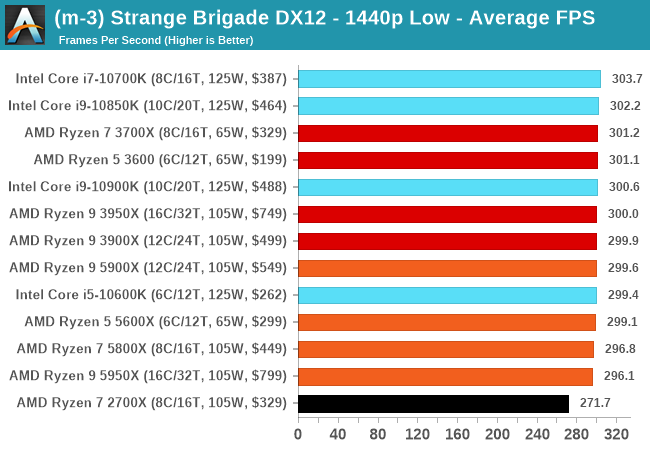 |
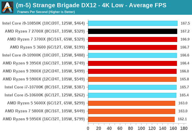 |
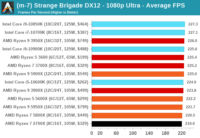 |
| 95th Percentile |  |
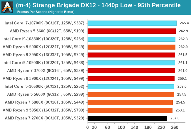 |
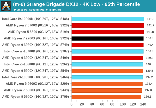 |
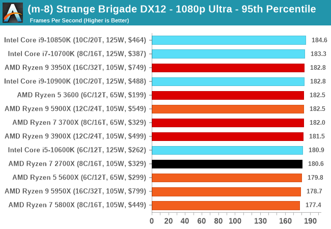 |
All of our benchmark results can also be found in our benchmark engine, Bench.
| AnandTech | Low Resolution Low Quality |
Medium Resolution Low Quality |
High Resolution Low Quality |
Medium Resolution Max Quality |
| Average FPS |  |
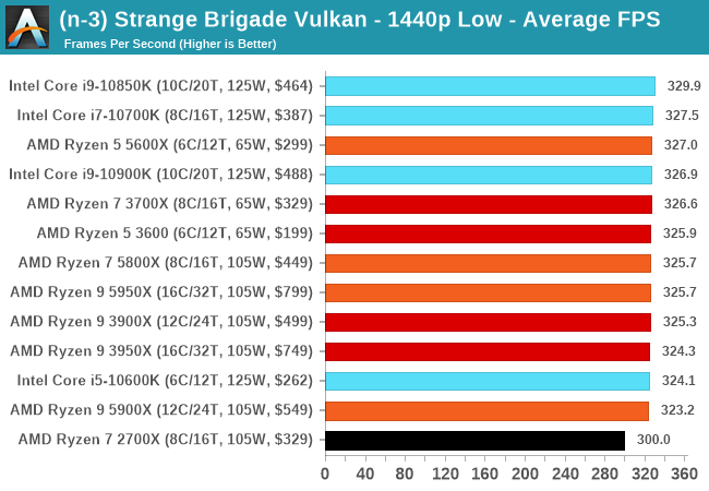 |
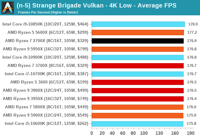 |
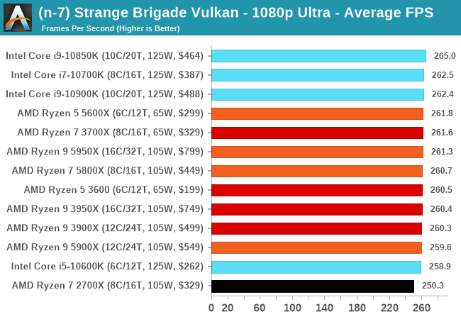 |
| 95th Percentile | 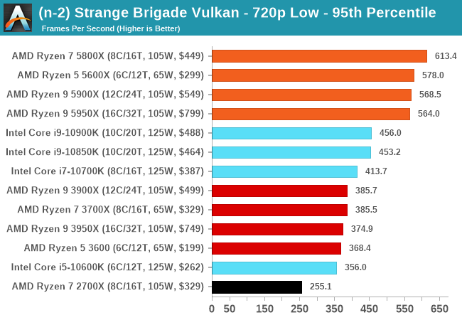 |
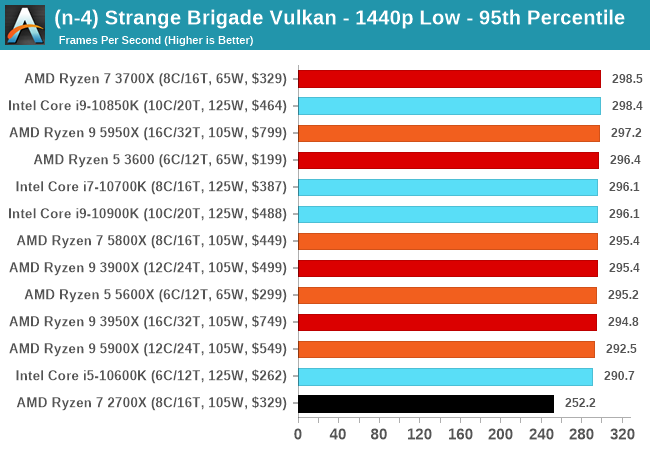 |
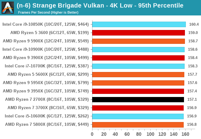 |
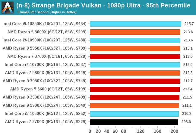 |
Conclusion: AMD Has Ryzen To The Top
Coming out the other end of this review, it’s hard to believe the extent to which some of AMD’s performance numbers have grown in the last five years. Even within the Ryzen family, we can pinpoint the leaps and bounds by which AMD is now the market leader in pure x86 performance.
Let’s start with some headline numbers.
+19% IPC Gain Confirmed
AMD quoted to us a raw IPC gain from Zen2 to Zen3 of +19%. AMD measured this with 25 workloads and both processors at 4.0 GHz, running DDR4-3600 memory. By comparison, we test with industry standard benchmarks at rated clock speeds and JEDEC supported memory, and we were able to accurately achieve that +19% number.
Compounding the generation-on-generation gains from a pre-Ryzen era, we’re seeing +114% IPC improvements, and if we look from the original Zen to Zen3, it is a ~41% gain.
In real world benchmarks, we saw an average +24% performance gain, showcasing both the increase in IPC and frequency uplift that the Ryzen 5000 parts have.
5.0 GHz Achieved on Ryzen
Turbo frequencies are often setup dependent, and because AMD uses a combination of listed turbo frequency and opportunistic boosting, the exact turbo frequency can be hard to nail down. For the top-tier Ryzen 9 5950X, AMD lists the turbo frequency as 4900 MHz for single core loading, however in very standard conditions, we were able to pass that to 5050 MHz. Diving deeper into the AGESA, this processor actually has a ‘maximum frequency’ setting of 5025 MHz. All of our Ryzen 5000 series processors offered +50-150 MHz above the listed turbo showcasing that these parts still have some headroom.
As we note in the review, AMD could have listed a 5 GHz turbo frequency, and it would be a big win for the company. However, I feel the company (a) wants to focus more on the market leading performance and engineering which doesn’t need 5 GHz, and (b) if they listed 5 GHz, it would suddenly be the only messaging people would take from the product launch. By not listing an explicit 5 GHz, it also allows AMD room to maneuver for a future product.
New WRs in Cinebench 1T, Breaking 10K in nT
AMD currently loves presenting CineBench as a measure of performance (Intel seems to flip/flop on the issue, depending on its position), and one of the main launch announcements was breaking the 600 point barrier in single threaded performance. At the time, it stated that the top three parts could get this value, whereas the Ryzen 5 5600X was just slightly behind.

In our testing, we scored at least 600 on all processors. This is significant as Intel’s latest Tiger Lake processors, turbo-ing at 4.8 GHz with as much power as they can use, only scored 595. Users that want a Tiger Lake can’t find one in a desktop, whereas the base Ryzen 5 5600X is $300.
Another win worth mentioning here though not explicitly announced by AMD is breaking the 10000 point barrier with the Ryzen 9 5950X in the multithreaded test. We achieved it just by the skin of our teeth, and a good few hundred points above AMD’s ‘reviewer guide’ that accompanies every launch. The only other CPUs to get above this value are 205 W Xeons or Threadrippers, while AMD does it within the 142 W peak power window.
Gaming: Cache is Good, But Depends on the Title
Performance in gaming is always a bit harder to pin down performance numbers, depending on the titles, resolutions, graphics card used, memory and drivers. AMD came into Zen3 showcasing a +5-50% gain at 1080p High over Zen2 across a number of titles, averaging 20-25%, along with performance leadership comparing against Intel’s best performer.
We don’t test at 1080p High, however we do have two metrics worth comparing. We run our games with an RTX 2080 Ti.
At the purely CPU-limited scenario, at the lowest resolutions and the lowest quality, we saw a +44% average uplift going from Zen2 to Zen3, from +10% on the low end to +80% on the high-end.
At 1080p Maximum, we saw a +10% average uplift going from Zen2 to Zen3. This varied from benchmarks where the results were equal due to being GPU-limited, to some modest +36% gains in more CPU-limited tests.
When we compare AMD against Intel, AMD easily wins the CPU-limited lowest resolution tests from +2% to +52%, averaging around +21% higher FPS. In the 1080p Maximum however, AMD and Intel trade blows, swaying from -4% to +6% for AMD (except in our Civ6 test, which is a +43% win for AMD).
As we saw in our recent Broadwell re-review, having access to large amounts of lower latency cache seems to be a good way to increasing gaming performance. By moving from each core having access to 16 MB to 32 MB, along with raw IPC gains, AMD is showing some good uplift. On the competitive front, we’re seeing a more even battlefield between Intel and AMD as the settings are cranked up.
Overall Impressions of Zen 3 and Ryzen 5000
One of the exciting things about probing a new core is finding out all the little quirks and improvements that they don’t tell you about. It’s been interesting finding out how this core was put together, both from our findings and discussions AMD’s engineers.
Moving to an 8-core CCX for this generation was a no-brainer, with an easy up-tick in performance. However it is the changes in the execution units and load/store were a lot of the magic happens – increasing to peak 3 loads/cycle and 2 stores/cycle, splitting out some of the ALU/AGU work, finer grained transitions from decoder/op-cache to the micro-op queue, and pre-fetchers with more bandwidth all help to that. A lot of the instruction improvements, such as lower latency FMA and faster DIV/IDIV is going to scale well as we move into the enterprise and EPYC processors.
With AMD taking the performance crown in almost area it’s competing in, attention now comes to price. Having $300 as an entry level for this tier is going to sting a lot of users who would rather spend $200 or less – despite AMD having nine out of ten of Amazon’s best sellers, only two of those parts are $300 and up. There’s going to be an early adopters tax as well – one could argue that moving into Q1, when AMD is enabling 400-series motherboards, might be a better inception point for a lot of users.
Having said that, with Intel set to launch Rocket Lake at the end of Q1 next year with 8 cores, this sub-$300 market is going to be ripe for any AMD Zen3 APU to come in and take that price bracket. AMD never launched Zen2 APUs into the consumer market, which might indicate a fast follow-on with Zen3. Watch this space – a monolithic Zen3 APU is going to be exciting.
| AMD Ryzen 5000 Series Processors Zen 3 Microarchitecture |
||||||
| AnandTech | Cores Threads |
Base Freq |
Turbo Freq |
L3 Cache |
TDP | MSRP |
| Ryzen 9 5950X | 16c/32t | 3400 | 4900 | 64 MB | 105 W | $799 |
| Ryzen 9 5900X | 12c/24t | 3700 | 4800 | 64 MB | 105 W | $549 |
| Ryzen 7 5800X | 8c/16t | 3800 | 4700 | 32 MB | 105 W | $449 |
| Ryzen 5 5600X | 6c/12t | 3700 | 4600 | 32 MB | 65 W | $299* |
All things considered, we’re really impressed with what AMD has achieved here. After the disillusionment of years of weaker generation-on-generation performance uplifts from the competition, AMD set a goal to beat the average ~7% IPC year-on-year gain. With +19% IPC on Zen3, Intel has no equal right now - not even Tiger Lake at 4.8 GHz - and has lost that single-threaded crown.
Zen3 gets a gold award. No question.

