Original Link: https://www.anandtech.com/show/16107/what-products-use-intel-10nm-superfin-demystified
What Products Use Intel 10nm? SuperFin and 10++ Demystified
by Dr. Ian Cutress on September 25, 2020 9:00 AM EST_678x452.jpg)
For our audience that regularly keeps track of Intel’s product portfolio, it would be hard to miss that the naming strategy of Intel’s process node technologies is a bit of a mess. To some, those words are themselves an understatement, as Intel has shifted its naming strategy 2-3 times since the launch of Intel’s first 10nm products. Not only that, even Intel’s various departments internally have a hard time keeping track of ‘what is this manufacturing process being called today’ when the press like AnandTech ask for details on the latest upcoming products.
Knowing this, and knowing what issues Intel has been having, I wanted to demystify Intel’s manufacturing process naming scheme such that users and engineers alike, even if they are inside Intel, can understand what is what but also importantly why. The why is the crucial factor.
If you're looking for a handy decoder ring for Intel's 10nm Products, it's here in page 3.
Why Do We Have Multiple Versions of a Process?
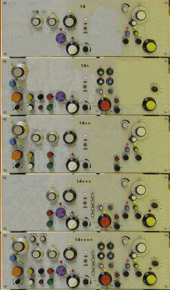
With Intel’s 14nm, we were invited to 14nm, 14+, 14++, 14+++, and if you believe Intel’s own slides, there were variants that went beyond this ++++ naming scheme. Each one of those additional + points on the end of the name signified a change in the process technology – usually to assist for increasing performance or efficiency.
Each one of these + points is an update to the BKM, or Best Known Methods.
While an engineer can draw an electrical layouts for a part of a processor, such as an addition circuit, actually applying that design to a silicon floorplan for manufacturing is a different skill altogether. Transistor libraries are designed to take advantage of a given process, and when a floorplan is optimized for a process, it can then be pasted and repeated as necessary – on top of this, simulation on thermals, power, and current density are applied to ensure that there are no hotspots or that critical paths inside the design have as few bottlenecks as possible.
When an update to the BKM occurs, two things can happen. Normally we see the update on the level of the transistor library that is changed – if the distance between two fins on a transistor increases for example, the transistor library and the macros may be made bigger, and then the floorplan might be redesigned to take account for this. As for any process node design, there are 100 different controls, and improving one might make three other controls worse, so it is a fine balancing act. Not only this, but the BKM has to be validated at the manufacturing level. The BKM update could apply to the metal stack as well, which in of itself can adjust the performance.
In the long long past, BKM updates were never advertised externally. If Intel or TSMC or another foundry discovered a way to improve the performance, or decrease the voltage, or improve the yield, the update was silently rolled into the design and nothing much was made of it. Sometimes processors would be listed as ‘1.0 volts to 1.35 volts’, and it would just be a roll of the dice if a user obtained one of the lower voltage models.
However, as time between different process node updates has elongated, these BKM updates have started to be identified and effectively monetized by the semiconductor companies. An update to a process that improves the voltage by 50 millivolts and increases frequency by 200 MHz immediately becomes a productizable event, and products built on these updates can be offered for more money over the usual. Or, depending on the rate of updates, the whole next generation of products could be built on the update.
So we never saw BKM updates officially announced at Intel’s 45nm, 32nm, or 22nm process nodes. These updates were fast enough that the productization of any update didn’t warrant a full round of marketing. With 14nm, that changed.
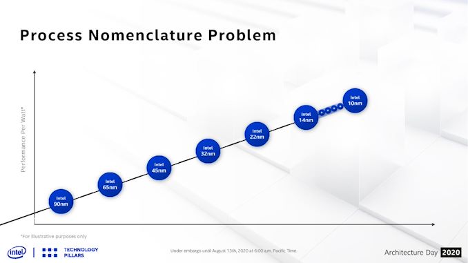
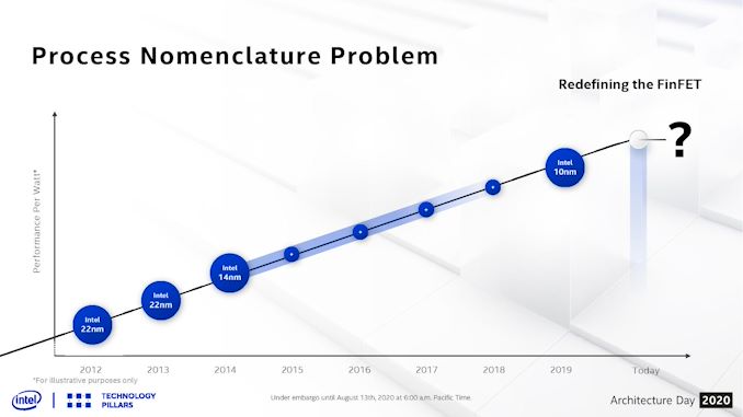
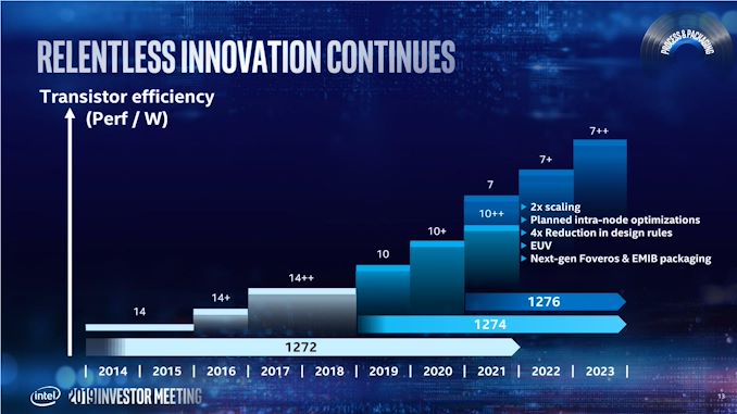
Intel had discussed its roadmap beyond 14nm since its 2010 Investor Meeting. It predicted that the company would be on 14nm by 2013, 10nm by 2015, and 7nm by 2017. As we now know, 14nm was two years late, and 10nm was 2-4 years late. Because of the introduction of 10nm being delayed, Intel decided to productize its 14nm BKM updates, and signified those with + points.
Intel’s current official line is that there have been four updates to 14nm, creating five ‘generations’.
More Plus Means More Meme
Because of all the + points, Intel’s marketing sometimes getting it wrong, and perhaps a little bit of ‘++’ in most programming languages meaning ‘+1’, the whole concept of adding + to the process node has become a meme – a meme at Intel’s expense, purely on the basis of its failure to deliver 10nm before the 14++++ naming scheme got out of hand.
10nm Takes a Different Tack: Cannon Lake to Ice Lake
In Intel’s own words, it shipped its first 10nm products for revenue by the end of 2017. These first processors, known as Cannon Lake, were shipped to a number of OEMs and stealthily hidden from the public, being pushed into commercial and educational products in China and others.
The processor had only two cores active, and the integrated graphics was broken, giving an indication of how well the first generation of 10nm was progressing. Intel had already committed to shipping 10nm for revenue by the end of 2017 to its investors, and the small side announcement at CES 2018 (it wasn’t mentioned in the keynote) followed by the small trickle of almost non-existent Cannon Lake product over 2018 technically fulfilled Intel’s obligation.
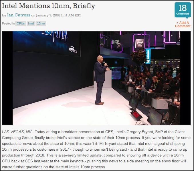 Click through to see the video
This version of 10nm didn’t get off the ground. Intel eventually put it into the Crimson Canyon NUC family in late 2018, but it was slower than the 14+++ processors it was meant to replace, and used more power.
At the time when Intel announced 10nm was shipping for revenue, it had already announced that the next generation product was going to be called Ice Lake, built on ‘10nm+’. By Intel’s Architecture Day in December 2018, the company tried to quietly rebadge Ice Lake as 10nm – when asked about the change and if this version of 10nm was any different to Cannon Lake, Intel’s Raja Koduri, partnered with Murthy Renduchintala, stated that ‘[10nm] is changing, but it hasn’t changed’. If ever there was a cryptic answer, this was it.
Ice Lake Rebadged to 10nm: Why?
So now we have Cannon Lake on ‘10nm’, and Ice Lake originally on 10+ but now rebadged to 10nm, but a different 10nm, with no real explanation as to why. In discussing with a number of peers and analysts in private conversations, the apparent conclusion they have come to is that Intel did not want to admit that its first generation of 10nm product had failed. Ever since then, Intel has attempted to quietly and discreetly shift Cannon Lake under the rug, as if it didn’t exist (it does exist, we did a big review on it, and Crimson Canyon is still for sale today at some of Intel’s biggest partners and major retailers).
Without Intel needing to admit that the first generation had failed, Ice Lake was the true ‘native’ 10nm product that was destined for life in the fast lane for consumers. If that was the case, then the low key presentation at CES 2018 stating it was shipping in 2017 was simply to meet investor targets. Intel never promoted Ice Lake as its first 10nm product, but the fact that the Cannon Lake product wasn't great meant that the company had to try and remove it from people's minds.
On Ice Lake, we studied the Ice Lake design, and we’ve seen lots of notebooks built on it. The fact that Intel called it ‘10th Gen’, and then also released the Comet Lake 14++++ product also called ‘10th Gen’, really ended up confusing the company even more, even in presentations to the press. It was the first time Intel had two products within the same generation of marketing name under different process nodes. It even confused OEM partner marketing teams as well as sales staff.
The problem with calling Ice Lake the new 10nm, is that internally the engineers still called it 10+. As Intel also announced other new products, such as Snow Ridge, or Lakefield, despite these meant to be called under the new 10nm, they would often be cited as ‘10+’ depending on which department of Intel you spoke to.
10nm Takes a Different Tack: Sapphire Rapids and Tiger Lake
In later 2019, during Intel’s HPC DevCon event focusing on supercomputers, the company discussed its post-Ice Lake server processor, Sapphire Rapids. It had already been announced that Sapphire Rapids was to power the Aurora supercomputer (which was originally supposed to have a 10nm Xeon Phi processor), however as part of the DevCon event we were discussion Sapphire Rapids in the context of a 10+++ process node. This event was mostly under the auspices of engineers, and those engineers were using 10+++ under the oldest naming scheme to identify Sapphire Rapids, or in other conversations, 10++. We were subsequently corrected by marketing in confirming that the official process node name was 10++; the engineers somewhat scoffed at this as a knock on effect to the Ice Lake name changing.
With the confusion on what to call these products between marketing and engineering, the discussions between the two (at least, from my perspective) didn’t really have any teeth at the time. Engineers didn’t either know about the new naming scheme, or didn’t understand why marketing had changed the names. Marketing wasn’t always there to correct engineering when speaking externally, and even if they were, sometimes the engineers wouldn’t understand the reasons why the names had changed. It starting to come to a head when Intel was discussing the product after Ice Lake, called Tiger Lake.
At CES 2020, the company announced Tiger Lake to the world in its Keynote address. As part of that keynote, as well as the press briefings, there was a lot of discussion as to whether this was a 10++ or 10+ product. People were getting confused between the old naming schemes and the new naming scheme, and whichever one was being used at the time.
I have continually had the conversation, especially at technical events, where I need to ask someone from Intel to clarify which scheme they were working under for any given product. For anyone outside of this bubble trying to keep track of it all, I can’t imagine what headaches you might have had – I was talking directly to Intel a lot of the time and it was giving me plenty of headaches! As Intel started announcing more 10nm-class products from different portfolio lines, each business unit had its own engineers in its own state of confusion. This came to a head when Intel changed the naming a second time.
No More Pluses, It’s All About SuperFin
As part of Intel’s Architecture Day 2020, the company did three things:
- Go into detail about Tiger Lake
- Go into detail about DG1 Xe Graphics, and new products in the portfolio
- Rename the different 10nm process node using SuperFin
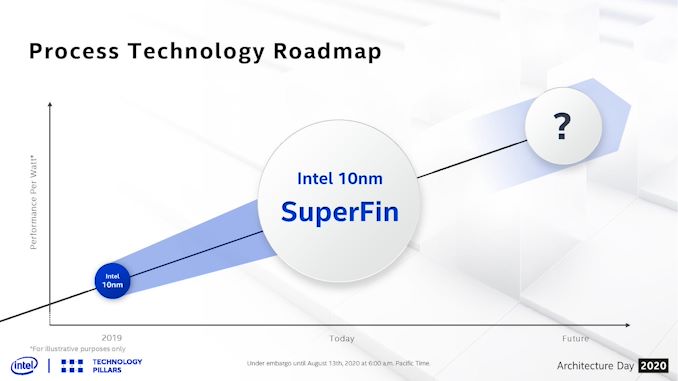
As part of that event, Intel went into some detail about its new ‘SuperFin’ technology. Using an updated metal stack and new capacitor technology, Intel had designated its latest BKM update for Tiger Lake and DG1 graphics as ‘10nm SuperFin’.
This is very much a marketing name, but the idea from the point of view of Intel’s communications team was to rebadge every 10nm product from Intel with some new variation of SuperFin as needed. This pushed Intel away from the ++++ nomenclature (something I’d advocated for anyway), and gave an opportunity for the company to realign all of its manufacturing branding with this new scheme.
While an interesting direction, Intel’s communications team has had two problems with this.
- Most/Some engineers were still working on the original naming scheme
- Some engineers/marketing were working on the first updated naming scheme and didn’t get the memo
Since changing from + and ++ to SuperFin, I have had a number of confusing calls with Intel’s engineers.
At Hot Chips in August, I was told by the presenter of the Ice Lake Xeon processors that the technology was an ‘enhanced 10nm’, which could have been meant as 10+, under the original naming scheme.
Even this week, for the launch of Intel’s new embedded Atom CPUs, I was told these CPUs were ‘10++’, without any indication of which naming scheme they were using. I was then told it was SuperFin. After the press release was changed for SuperFin, and we published our article, it was noticed that Intel's own product database had it listed as regular 10nm, no SuperFin. It turns out that it was regular 10nm, no SuperFin, the same as Ice Lake.
Even when directly discussing with Intel’s communication teams, they would start referring to the original naming scheme, or the first updated scheme. I've had to request double confirmation on multiple occasions. While Intel has a main HQ communications team, each business unit inside Intel has its own PR people. Each business unit may also be working with a PR agency (sometimes different to each other), and then beyond that, there may be different PR connections for each region, and then each with its own localized PR company. Renaming a product or a process is thus a very hard thing to force down every channel, compared to a new product which should have the right name on the initial documents.
When speaking with Intel’s lead Tiger Lake engineers in a 1-on-1 interview, I asked them outright if the new SuperFin naming scheme was being used by the engineering teams. I was told that for the most part, it was. I followed up asking if mistakes and slip ups were made, and the answer came back in the affirmative. It’s somewhat clear that the Engineering teams don’t like being pushed around by the marketing/communications teams in this way, having to change internal documents and naming processes in order to internalize what stuff is being called when it can’t be called what it originally was almost a decade ago. We see the same thing when engineers are rolled out to present about new products – they will call the processors by the internal code names, not ‘Core 10th Gen’ or similar, and often have to stop themselves by continually saying the code name.
The AnandTech Decoder Ring for Intel 10nm
The reason why I’m writing about this topic is because it is all a bit of a mess. Intel is a company so large, with many different business units each with its own engineers and internal marketing personnel/product managers, that a single change made by the HQ team takes time to filter down to the other PR teams, but also filter back through the engineers, some of which make press-facing appearances. That’s before any discussions as to whether the change is seen as positive or negative by those affected.
I reached out to Intel to get their official decoder ring for the 10++ to new SuperFin naming. The official response I received was in itself confusing, and the marketing person I speak to wasn’t decoding from the first 2018 naming change, but from the original pre-2017 naming scheme. Between my contacts and I we spoke over the phone so I could hear what they wanted to tell me and so I could tell them what I felt were the reasons for the changes. Some of the explanations I made (such as Intel not wanting to acknowledge Ice Lake 10nm is different to Cannon Lake 10nm, or that Ice Lake 10nm is called that way to hide the fact that Cannon Lake 10nm didn’t work) were understandably left with a no comment.
However, I now have an official decoder ring for you, to act as a reference for both users and Intel’s own engineers alike.
| AnandTech's Decoder Ring for Intel's 10nm | ||||
| Product | 2020+ | First Update |
Original |
|
| Cannon Lake | - | - | 10nm | |
| Ice Lake Ice Lake-SP Lakefield (compute) Snow Ridge Elkhart Lake |
10nm | 10nm | 10+ | |
| Tiger Lake SG1 DG1 |
10nm Superfin |
10+ | 10++ | |
| Alder Lake First Xe-HP GPU Sapphire Rapids |
10nm Enhanced SuperFin |
10++ | 10+++ | |
For clarity, 10nm Superfin is often abbreviated to 10SF, and 10nm Enhanced Superfin to 10ESF.
Moving forward, Intel’s communications team is committed to explaining everything in terms of 10nm, 10SF, and 10ESF. I have been told that the process of moving all internal documents away from the pre-2017 naming to the 2020 naming is already underway.
We reached out for Intel for a comment for this article:
It is widely acknowledged within the industry that there is inconsistency and confusion in [our] nanometer nomenclature. Going forward, we will refer the next generation 10nm products as 10nm SuperFin technology-based products.
My take is that whoever had the bright idea to knock Ice Lake down from 10+ to 10 (and then Tiger from 10++ to 10+ etc.), in order to protect the company from addressing issues with the Cannon Lake product, drastically failed at predicting the fallout that this name change would bring. Sometimes a company should accept they didn't score as well as they did, admit the hit, and move on, rather than try and cover it up. So much more time and effort has been lost in terms of communications between the press and Intel, or the press and engineers, or even between the engineers and Intel's own communications team. Even the basic understanding of dealing with that change has been difficult, to the detriment of the press trying to report on Intel’s technology, and likely even on the financial side as investors try to understand what’s going on.
But, truth be told, I’m glad that Intel moved away from the ++++ nomenclature. It allows the company to now easily name future manufacturing node technologies that aren’t just for pure logic performance, which may be vital if Intel ever wants to become a foundry player again.

