Original Link: https://www.anandtech.com/show/15706/ceva-announces-senspro-new-high-performance-sensor-hub-ip
CEVA Announces SensPro - New High Performance Sensor Hub IP
by Andrei Frumusanu on April 7, 2020 11:30 AM EST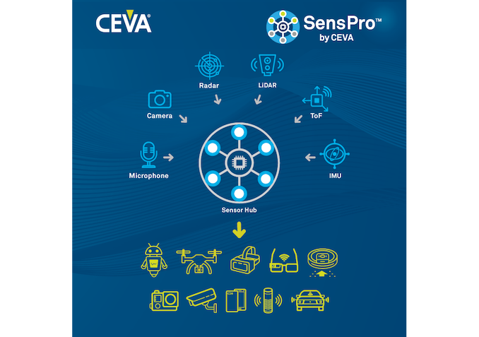
As devices become ever more interconnected and increase their capabilities to sense the world through different kind of sensors, there’s an ever more increasing stream of data that is being created. Naturally, not all of that data is useful, with the vast majority of it being thrown away. To differentiate between useful data and less useful noise, there’s an increasing need for processing power on the part of the brains of newer generation devices.
In the past generally we’d have more simplistic sensors such as microphones or accelerometers being the main data sources, and that’s where we usually know the term of “sensor hub” from – when mobile devices first trying to optimise the handling of smartphone sensors. First these were discrete chips, but later on they have been integrated into SoCs.
As data complexity rises, and as new and more complex sensors types appear, CEVA sees to address the need for higher performance sensor hubs. Today’s announcement is about the new SensPro IP family from CEVA, offering a new IP architecture that leverages the company’s existing IP expertise, combining various processing capabilities and flexibility into one single self-contained product offering.
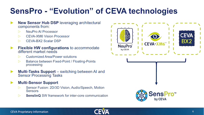
SensPro is a ground-up design that focuses on maximising power efficiency, combining processing designs that were found in CEVA’s NeuPro designs in terms of ML capabilities, the XM6 image processing prowess, as well as the company’s in-house BX2 scalar DSP microarchitecture which serves as the control unit for the whole new IP.
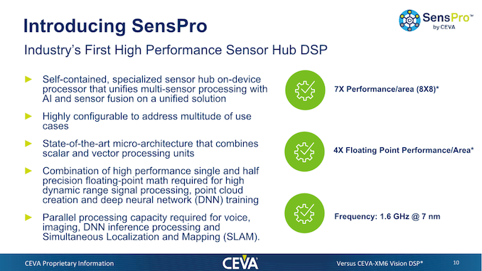
The idea to combine these elements of what are usually different individual IPs into a single processing block is said to be a first in the industry – hence their calling It the first ever “High performance sensor hub DSP”. The goals here are extremely high in terms of the flexibility of the design and what kind of use-cases it’s meant to be deployed in. Usually we think as smartphone being the first such use-case, but it’s actually more in other areas where a device wouldn’t have as high processing capabilities where we’d see the SensPro have a larger impact in. Quoted are use-cases of robotics, automotive, AR/VR headsets, voice assistants, smart home devices and more importantly new industrial applications where we’re seeing a larger shift to more integrated and smarter automation in areas such as production lines.
Combining scalar and vector processing into one IP, with the ability to also process floating-point operations is quite unique – well you’d think a CPU could do that as well, but here CEVA’s advantages lie in their ability to do all of this extremely efficiently in a low-power design.
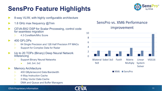
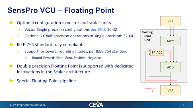
From a performance standpoint, the new SensPro is a major architectural upgrade over what was previously offered by familiar IP such as the XM6. CEVA here quoted figures such as 400 GFLOPs of power on a 1.6GHz design target in terms of FP performance, achieved through either 64 32-bit FP MAC operations or 128 16-bit ops. FP capability is said to be important for higher precision arithmetic use-cases where higher dynamic range is required, Radar being one data type that is being brought up in this context.
There’s also the fixed-point vector processing pipelines whose configuration contains up to 1024 8x8 MACs, allowing for up to 3 TOPs 8x8 inferencing. CEVA actually also has an execution mode for binary neural networks and promises here up to 20TOPs inferencing throughput, which is a wild number, but we have to remember that this only to applies to specific models that are able to work with only 2-bits of data.
The IP’s data bandwidth capabilities are actually quite massive, employing a super-wide 2048-bit load unit alongside a 1024-bit store unit, which corresponds to 400GB/s of data ingestion and 200GB/s of output. It sounds like a lot, but we have to remember that the IP would be handling immense data streams coming from a myriad of different sensors.
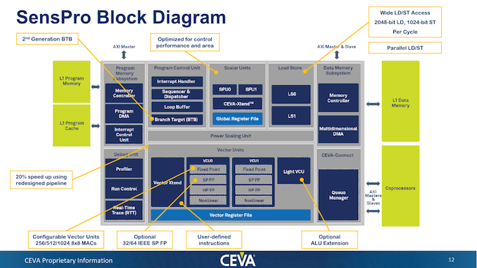
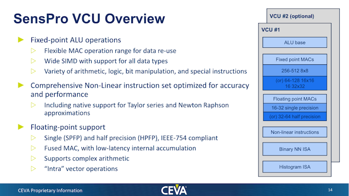
From a high-level perspective, what’s important to note in the block diagram is the configuration flexibility that the IP offers. Generally, amongst the processing units, the scalar processors as well as one vector processing unit are the minimum configuration of the design. Within a vector unit though things can quite a bit more complicated:
A SensPro VCU consists of different execution units handling either fixed point MACs, floating point MACs, or other specifically dedicated special function units for their specific instructions.
The configurability for customers is even more fine-grained than just choosing the amount and type of units that’s integrated into the IP, in the floating point units for example CEVA also gives one the choice between different throughput designs, with a choice of doubling the single-precision throughput to the optional possibility of doubling throughput again for FP16 operations.
CEVA’s initial IP configurations consists of 3 designs – the SP250, SP500F and SP1000, with each incremental step corresponding to the 8-bit MAC configuration.
- SP250 – single vector unit with 256 8x8 MACs targeting imaging, vision, and sound centric applications
- SP500F – single vector unit with 512 8x8 MACs and 64 single precision floating point MACs targeting SLAM centric applications
- SP1000 – dual vector units with 1024 8x8 MACs and binary networks support targeting AI centric applications
The SP500F is the only starting design that implements the floating-point execution units and is more targeted towards vision and SLAM use-cases with radar or LIDAR. For consumer electronics we’ll most likely see the SP250 being used in devices such as smartphones, IP cameras and other similar products.
Ran Snir, Vice President of Research and Development at CEVA, commented:
“With the growth in the number and variety of sensors in modern systems, and their substantially different computation needs, we set out to design a new architecture from the ground up to address this challenge. We constructed SensPro as a highly configurable, holistic architecture that could handle these intensive workloads using a combination of scalar, vector processing and AI acceleration, while utilizing the latest micro-architecture design techniques of deep pipelining, parallelism, and multi-tasking. The result is the most powerful DSP architecture ever conceived for sensor hubs and we’re truly excited to work with our customers and partners to bring contextually-aware products to market based on it.”
The IP is targeted for general licensing in Q3 2020 – meaning it’ll be a few years before we see any kind of silicon design-ins and even products with the new IP.

