Original Link: https://www.anandtech.com/show/1561
915 Motherboard Roundup: Socket 775 for the Rest of Us
by Wesley Fink on December 7, 2004 12:25 AM EST- Posted in
- Motherboards
Intel launched the new Pentium 4 Socket 775 processors and the 925X/915 chipsets to support them on June 19th. Since that time, the demand for the new Intel motherboards has been underwhelming, to say the least. The new Intel architecture launched many new technologies and features to the market. We explored these new features in the launch reviews: Intel 925X/915: Chipset Performance & DDR2 and Intel's 925X & LGA-775: Are Prescott 3.6 and PCI Express Graphics any Faster? The bigger issue, though, is that the Intel 925X/915 didn't also bring with them a compelling reason for users to embrace the new socket or the new features.
The new 775 processors just weren't any faster than the Socket 478 CPUs most owned already. So for the same performance, users would need a new processor on a new motherboard, new DDR2 memory, a new heatsink/fan, a new PCI Express video card to replace their AGP video card, and (most likely) a new power supply with a 24-pin power connector. For this, they get about the same performance with a hotter-running 90nm CPU that has developed a reputation for throttling unless the HSF and thermal compound is exactly right. Unless manufacturers found ways around the design issues with 925X/915, buyers also found that they were moving from the best overclocking platform in the Socket 478 to a limited OC solution in Socket T. Fortunately, many manufacturers found ways around this issue. However, you will see in this roundup that there are still manufacturers who did not make revisions to get around the 10% Overclock limit.
As a result of all this, we have not looked any further at Socket T after our initial run at the top 925X boards in Intel 925X Roundup: Creative Engineering 101. Now, some 6 months later, there are market developments that make it worthwhile to look at mainstream 915 boards. The most important of these is that Intel is tightening supplies of 865/875 chipsets to move buyers to the new socket. Manufacturers are finding it more difficult to find 865/875 chipsets to buy, or in some cases, they must buy a Socket T chipset with every 865/875 chipset that Intel will sell them. The time is coming when your only choice from Intel will be one of the new 915/925X boards. We also found that the variation in performance among new 915 boards is much greater than what we have seen in any recent chipset, so it is time for a little guidance on what performs best. If the only choice is 915, you need to know how the huge selection of Socket T boards will actually perform in a head-to-head comparison.
The Roundup
The 13 motherboards in this roundup represent a larger group of around 23 motherboards. We decided to eliminate those boards from the same manufacturers that differed only in offering on-board graphics with the 915G chipset. We covered Intel integrated graphics performance in Intel 915 Graphics: Graphics Media Accelerator 900 and all of the 915G boards that we had for testing did have both integrated graphics and a PCI Express slot for a video update. If you're looking for integrated graphics, consider the performance data in this roundup relevant to the same manufacturer's 915G board with the addition of integrated graphics.If you're interested in comparing integrated graphics, then the 915G review and the recent ATI Radeon Xpress 200 launch review should provide the information you're looking for on integrated graphics performance. Please keep in mind that 915G boards, geared to entry level systems and the business desktop, may perform the same as the 915P boards from the same manufacturer, but they often have more limited options in BIOS. Enthusiasts generally prefer higher performing graphics solutions in an AGP or PCIe video card, and these are the same buyers who also demand better options for tweaking the performance of their motherboard.
One other consideration is memory. All of the 925X boards used the new DDR2 memory, but the 915 chipset family can use either DDR2 or DDR memory. A couple of manufacturers, Gigabyte and DFI, decided to provide the ability to use either DDR or DDR2 memory, but even so, you cannot use both at the same time. This added flexibility is great if you have DDR now, yet plan to move to DDR2 in the future, but it does come with a price. Both boards are limited to 2GB of memory, which can be either DDR2 or DDR instead of the 4GB maximum for single memory boards.
The rest of the boards in the roundup use either DDR2 or DDR. You will find DDR2 featured on the AOpen, Asus, ECS, Foxconn, and MSI. The rest of the manufacturers decided to build their 915 boards with an easier upgrade path and DDR400 memory. This includes Abit, Albatron, Biostar, Epox, Jetway, and Soltek. Since the type of memory that can be used on a 915 board matters a great deal to many buyers, we have tried to group the test results so that you can identify the memory capabilities easily. Color codes were used in our graphs to make it easy to spot DDR, DDR2 and DDR/DDR2 motherboards. The color codes are described in detail in the Test Configuration on page 29.
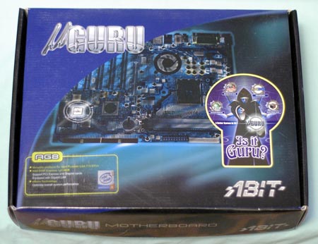
Abit AG8: Features and Layout
| Abit AG8 Motherboard Specifications | |
| CPU Interface | Socket 775 Pentium 4 (Prescott) |
| Chipset | Intel 915P/ICH6R |
| BUS Speeds | 100MHz to 400MHz (in 1MHz increments) |
| DDR Speeds | Auto, 333, 400 |
| PCI Speeds | 33.33, 36.36, 40.00 |
| Core Voltage | CPU Default to 1.7375V in 0.0125V increments |
| DRAM Voltage | 2.5V to 3.2V in 0.05V increments |
| NB (Northbridge) Voltage | 1.50V-2.05V in 0.05V increments |
| Memory Slots | Four 184-pin DDR 400 Slots Dual-Channel Unbuffered Memory to 4GB |
| Expansion Slots | 1 PCIe x16 Slot 3 PCIe x1 slot 2 PCI Slots |
| Onboard SATA/IDE RAID | 4 SATA 150 drives by ICH6R Can be combined in RAID 0, 1, Intel Matrix |
| Onboard IDE | One Standard ATA100/66 (2 drives) |
| Onboard USB 2.0/IEEE-1394 | 8 USB 2.0 ports 3 IEEE 1394 FireWire Ports by TI 4200R7T |
| Onboard LAN | Gigabit PCI Ethernet by Realtek 8110S-32 |
| Onboard Audio | AC'97 2.3 Realtek ALC658 8-Channel with SPDIF in/out |
| Tested BIOS | 1.7 Award |
With a name like AG8, you may be tempted to conclude that this must be an integrated graphics board, but in fact, the Abit AG8 is based on the Intel 915P chipset. You can certainly see the family resemblance to the Abit AA8 DuraMAX, which is one of the better performing 925X motherboards - and that is a good thing. Abit has included the ICH6R south bridge, which brings Intel Matrix RAID to the AG8. This is something many other boards in our roundup neglect as they choose the non-Raid ICH6 to save a few dollars on the cost of their 915 board. Abit also kept the Firewire ports on the AG8 - another area that is often cut to price down the 915 for the mainstream.
Abit made concessions to a price point on the AG8 in their choice of an average AC'97 2.3 audio solution instead of the extremely capable Azalia High-Definition audio. You will find Gigabit LAN on the AG8, but it is the version tied to the PCI bus instead of the faster PCI Express version. These concessions will matter to some and not much to others, but it does help Abit keep the price competitive in what they hope will be a very active market segment.
Abit has included their typical wide selection of voltages and frequencies to get the most from the AG8 and the Pentium 4 Prescott. Abit was one of the first motherboard makers to break through the overclocking limitations of the 925X chipset, and this is also reflected in the 915P AG8 where additional automatic manipulations are being made by µGuru at boot. The PCIe frequency is adjusted dynamically in relation to the CPU frequency prior to boot, to allow a higher overclock with the AG8. The overclocking controls are typically Abit, which means exceptionally wide ranges in BIOS compared to most other boards in the 915 roundup. Abit decided not to include PCI Express speed adjustments in the BIOS - they are being manipulated in µGuru instead.
The voltage adjustments for memory are particularly noteworthy, since they extend to 3.2V. This should be enough to satisfy most DDR users and it even provides options to use some of the fast high-voltage memory, which has recently been introduced to the High-end memory market. The range of available voltages for the CPU and Northbridge are also stands out - as you would expect from a company that so closely identifies with the computer enthusiast The Northbridge adjustments extend from the default 1.5V all the way to 2.05V, which is a wider range than what you find on any other board. As we saw on the AA8 Duramax, Abit has added a hefty heatsink with a side-blowing fan to the northbridge to handle the voltage range that they have built into the AG8.
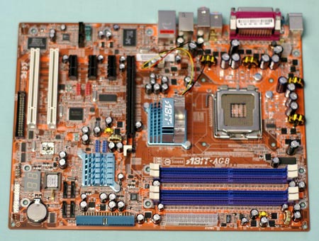
Abit uses a flat edge connector for the single IDE connection provided by the 915P chipset, which can be a difficult fit in most mid-tower cases. We suggest that you connect the IDE cable before you mount the board, since the connector falls under the hard drives in many case designs and is difficult to reach after the board is screwed down. We generally like the idea of edge connectors, but some case designs make it very difficult to connect the edge-connectors. If you still use a floppy, you will find the location to be a real problem at the very bottom center of the motherboard. When you try to route the floppy cable to clear the 4 SATA connectors, it tends to hide the diagnostic LEDs and interfere with the front-panel connectors. The bulky 24-pin power connector is on the right board edge and the 4-pin 12V connector is on the top board edge. Both these locations are excellent - you will not have to fish cables over or around the CPU. The Abit trademark 2-digit diagnostic LEDs are also found on the mainstream-priced AG8. They can be very useful for troubleshooting.
Abit uses the Realtek ALC658 codec instead of an Intel HD compliant audio codec on the AG8. You have to save money somewhere, but the HD audio is a trademark 925X/915 feature and it is a shame to lose this great feature. You can find more information on the features and specifications of the Realtek 658 at the Realtek website. While you're there, you should also do a little research on the High-Definition audio codecs also supplied by Realtek.
Abit AG8: Overclocking and Stress Testing
FSB Overclocking Results
Intel has recently talked about Speedstep, which is the ability of Prescott processors to run at both stock speed and a lower 14X multiplier. Speedstep works on most 925X motherboards and it has recently been added to some 915 motherboards with BIOS updates. This capability will likely be added to other 915/925X motherboards in the future. For that reason, all overclocking tests were performed at a stock 3.6GHz (18X) on motherboards in this roundup and at 14X, the Speedstep multiplier.| Front Side Bus Overclocking Testbed | |
| Processor: | Pentium 4 Prescott LGA 775 560 ES (2.8GHz-3.6GHz) |
| CPU Voltage: | 1.425V (1.3675V default) |
| Cooling: | Thermaltake Jungle 502 |
| Power Supply: | OCZ Power Stream 520 |
| Maximum CPU OverClock: | 222x18 (3996MHz) +11% |
| Maximum FSB OC: | 261FSBx14 (+31%) |
The results of the Abit overclocks look impressive until you compare them to boards like the DFI, Asus, or MSI. It is fair to say that overclocking with the Abit AG8 is above average, but not the top of the roundup. The 261 wall is similar to the issues that we found with SATA drives on the Asus AA8 - you run into a wall with SATA around 260 on the Abit and you just can't break around it. The Abit AG8 will go higher in overclocking if you plan to use it with an IDE drive, but this can prove to be a challenge with just one IDE connector available for all your optical drives and a hard drive.
The AG8 was able to achieve a FSB of 261, a 31% overclock, with an ATI X800 XT and SATA hard drive. Abit manipulates the PCIe frequency with uGuru during boot to achieve higher overclocks. For more information on how Abit manages to overclock the AA8/AG8, please check Breaking Intel's Overclock Lock: The REAL Story.
Memory Stress Test Results:
The memory stress test measures the ability of the Abit AG8 to operate at its officially supported memory frequency (400MHz DDR) at the best performing memory timings that OCZ PC3200 Platinum Rev. 2 will support. Memory stress testing was conducted by running the DDR400 with 2 DIMM slots operating in Dual-Channel mode.| Stable DDR400 Timings - 2 DIMMs (2/4 DIMMs - 1 Dual-Channel Bank) |
|
| Clock Speed: | 200MHz |
| Timing Mode: | 1:1 (200:200 - Default) |
| CAS Latency: | 2.0 |
| Bank Interleave: | Auto |
| RAS to CAS Delay: | 2 |
| RAS Precharge: | 2 |
| Cycle Time (tRAS): | 5 |
The Abit AA8 DuraMAX was completely stable with 2 DIMMs in Dual-Channel at the DDR settings of 2-2-2-5, at 2.6V default voltage.
Filling all four available memory slots is more strenuous on the memory subsystem than testing 2 DDR modules on a motherboard.
| Stable DDR400 Timings - 4 DIMMs (4/4 DIMMs - 2 Dual-Channel Banks) |
|
| Clock Speed: | 200MHz |
| Timing Mode: | 1:1 (200:200 - Default) |
| CAS Latency: | 2.0 |
| Bank Interleave: | Auto |
| RAS to CAS Delay: | 2 |
| RAS Precharge: | 2 |
| Cycle Time (tRAS): | 5 |
The Abit uses familiar DDR memory and performed much as we have come to expect with 4 DDR400 DIMMs. With 4 DIMMs, the Abit was stable at the same aggressive 2-2-2-5 timings that we found with 2 DIMMs.
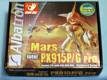
Albatron PX915P Pro: Features and Layout
| Albatron PX915P Pro Motherboard Specifications | |
| CPU Interface | Socket 775 Pentium 4 (Prescott) |
| Chipset | Intel 915P/ICH6 |
| BUS Speeds | 200MHz to 333MHz (in 1MHz increments) |
| DDR2 Speeds | Auto, 333, 400 |
| PCI Speeds | 33.33, 36.36, 40.00 |
| Core Voltage | 0.8375 to 1.60V in 0.0125V increments plus 1.6 to 1.9V in 0.1V increments |
| DRAM Voltage | Default, +.1V, +.2V, +.3V, +.4V |
| NB (Northbridge) Voltage | Default, +.1V, +.2V, +.3V |
| Memory Slots | Four 184-pin DDR 400 Slots Dual-Channel Unbuffered Memory to 4GB |
| Expansion Slots | 1 PCIe x16 Slot 3 PCIe x1 slot 2 PCI Slots |
| Onboard SATA/RAID | 4 SATA 150 drives by ICH6 |
| Onboard IDE/RAID | One Standard ATA100/66 (2 drives) plus ITE IT8281 (4 drives) ITE can be combined as RAID 0, 1, 0+1, JBOD |
| Onboard USB 2.0/IEEE-1394 | 8 USB 2.0 ports No FireWire Ports |
| Onboard LAN | Gigabit PCI Ethernet by Marvell MV8001 10/100 Ethernet by VIA VT6105 |
| Onboard Audio | Realtek ALC880 (HD Audio) 8-Channel with SPDIF in/out |
| Tested BIOS | 1.19 Award |
Albatron has been very aggressive in their marketing of 915/925X solutions. The PX915P Pro represents the top 915 board aimed at the enthusiast. There are other boards in the Albatron 915 lineup, most notably, thePX915G Pro, which is the same board based on the integrated graphics G version of the 915 chipset. Albatron also offers both the P and G 915 boards without the Pro designation. These non-Pro boards are cheaper and don't have firewire.
None of the Albatron 915 boards are offered with the ICH6R chipset - they all use the non-RAID ICH6 south bridge. Albatron does, however, include Intel High-Definition audio (Azalia) in even the cheapest 915 board that they offer. Interestingly, all 4 boards also offer support for 4 additional IDE drives to supplement the limited 2 IDE drives provided by the 915 chipset. The point is that Albatron made some smart decisions on cost reduction in our opinion. HD audio and additional IDE ports are features that we like to see on all the boards. You will be disappointed that to get Intel Matrix RAID, you will need to choose the Albatron 925X.
As the 915 flagship, the PX915P Pro offers a very wide range of options in the Award BIOS. Noteworthy is the incredible CPU voltage range to a dangerous 1.9V for a 1.3875V Socket T CPU. However, water-cooling and phase change overclockers will like to see such a wide range in a stock BIOS. Other BIOS options are also generous for tweaking with memory voltage reaching to 3.0V and the north bridge voltage selectable to +0.3V.
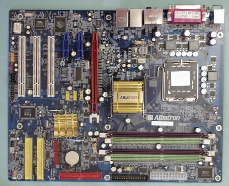
Layout of the PX915P Pro is very good. It's good to see the floppy connector in a usable upper right edge location. The 24-pin ATX is also at the board's right edge and the IDE is located on the edge as well. It is located a little lower than what we like, just below mid-line, but the location still works well in most case designs. The 4-pin connector is a little less accessible, located about mid-board between the CPU and IO backplane. You have to be careful when you route the 4-pin 12V cable, but it is also pretty easy to get a 4-pin cable of the way of cooling. With 4 SATA connectors and 2 additional IDE ports on the lower right edge behind the slots, you have a busy board, but you rarely see full-length cards any more. The PCIe x16 slot is still clear to handle even the biggest video card.
Albatron uses the capable Realtek ALC880 codec for High Definition 8-channel audio. This is the same High-Definition audio codec that we saw used in most motherboards in the 925X roundup, so it speaks well of Albatron's HD choice. Realtek says that their 7.1 Channel High Definition Audio features four 24-bit two-channel DACs and three stereo 20-bit ADCs. "The ALC880(D) also achieves 100dB sound quality; easily meeting PC2001 requirements and also bringing PC sound quality closer to consumer electronic devices." You can find more information on the features and specifications of the Realtek 880 at the Realtek website.
Albatron PX915P Pro: Overclocking and Stress Testing
| Front Side Bus Overclocking Testbed | |
| Processor: | Pentium 4 Prescott LGA 775 560 ES (2.8GHz-3.6GHz) |
| CPU Voltage: | 1.425V (1.3675V default) |
| Cooling: | Thermaltake Jungle 502 |
| Power Supply: | OCZ Power Stream 520 |
| Maximum CPU OverClock: | 222x18 (3996MHz) +11% |
| Maximum FSB OC: | 250FSB x 14 (+25%) |
The Albatron 915P Pro was an above-average performer in our overclock tests, reaching 3996MHz at the stock 18X multiplier. At the Speedstep 14X ratio, the Albatron performed fine to a 250 FSB setting. Above 250, the SATA drive disappeared and it was not possible to boot at higher FSB settings. Since the Albatron continued to boot to the hard drive initialization stage at higher FSB, the Albatron may reach higher overclocks with an IDE drive.
A few weeks after the launch of the Intel 915/925X chipsets, Albatron made some claims that the key to high overclocks on the 915 chipset was increasing Northbridge voltage. We did not find that further increases in NB voltage allowed any higher overclock with SATA drives - 250 was the limit for our components on the Albatron. For more information on how others manage to overclock the 915/925X, please check Breaking Intel's Overclock Lock: The REAL Story.
Memory Stress Test Results:
The memory stress test measures the ability of the Albatron PX915P Pro to operate at its officially supported memory frequency (400MHz DDR), at the best performing memory timings that OCZ PC4200 Platinum Rev. 2 will support. Memory stress testing was conducted by running DDR at 400MHz (stock 1:1 ratio) with 2 DIMM slots operating in Dual-Channel mode.| Stable DDR400 Timings - 2 DIMMs (2/4 DIMMs - 1 Dual-Channel Bank) |
|
| Clock Speed: | 200MHz |
| Timing Mode: | 1:1 (200:200 - Default) |
| CAS Latency: | 2.0 |
| Bank Interleave: | Auto |
| RAS to CAS Delay: | 2 |
| RAS Precharge: | 2 |
| Cycle Time (tRAS): | 5 |
The Albatron was completely stable with 2 DIMMs in Dual-Channel at DDR400 settings of 2-2-2-5 at 2.6V default voltage. These are the fastest settings available with the DDR400 test DIMMs.
Filling all four available memory slots is more strenuous on the memory subsystem than testing 2 DDR2 modules on a motherboard.
| Stable DDR400 Timings - 4 DIMMs (4/4 DIMMs - 2 Dual-Channel Banks) |
|
| Clock Speed: | 200MHz |
| Timing Mode: | 1:1 (200:200 - Default) |
| CAS Latency: | 2.0 |
| Bank Interleave: | Auto |
| RAS to CAS Delay: | 2 |
| RAS Precharge: | 2 |
| Cycle Time (tRAS): | 5 |
The system was stable with 4 DIMMs at the same aggressive settings used for 2 DIMMs.
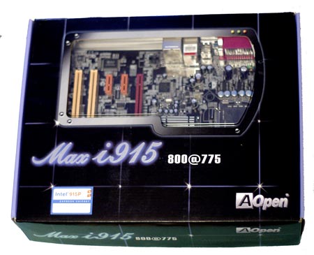
AOpen i915Pa-EFRII: Features and Layout
| AOpen i915Pa Motherboard Specifications | |
| CPU Interface | Socket 775 Pentium 4 (Prescott) |
| Chipset | Intel 915P/ICH6R |
| BUS Speeds | 100MHz to 400MHz (in 1MHz increments) |
| DDR2 Speeds | Auto, 400, 533 |
| PCI Speeds | 33.33, 36.36, 40.00 |
| Core Voltage | 1.4375V to 1.7875V in 0.0125V increments |
| DRAM Voltage | 1.80V to 1.95V in 0.05V increments |
| NB (Northbridge) Voltage | 1.50V-1.65V in 0.05V increments |
| Memory Slots | Four 240-pin DDR2 533 Slots Dual-Channel Unbuffered Memory to 4GB |
| Expansion Slots | 1 PCIe x16 Slot 2 PCIe x1 slot 3 PCI Slots |
| Onboard SATA/IDE RAID | 4 SATA 150 drives by ICH6R Can be combined in RAID 0, 1, Intel Matrix plus 2 SATA by Promise 20579 |
| Onboard IDE | One Standard ATA100/66 (2 drives) One Promise 20579 (2 drives) |
| Onboard USB 2.0/IEEE-1394 | 8 USB 2.0 ports 2 IEEE 1394 FireWire Ports by TI42AK0KT |
| Onboard LAN | Gigabit PCIe Ethernet by Broadcom BCM5751 |
| Onboard Audio | Realtek ALC880 (HD Audio) 8-Channel with SPDIF in/out |
| Tested BIOS | R1.01A Award |
AOpen lists a wide range of 915 motherboards that are sold into different areas of the world. The AOpen board tested was a very full-featured model called the i915Pa-EFRII. Packaging used a windowed box and a clear internal clamshell to show off the actual board that you are buying. The overall look reminds us of past Abit top-line, as it is similar to the Abit MAX series.
AOpen generally provides a wide range of BIOS tweaking controls on the i915Pa. The range on FSB and CPU voltage is particularly wide and should satisfy most users. However, the very small range of 1.8V to 1.95V for memory voltage is really not enough for most enthusiasts. As you will see in our overclocking tests, however, this is all a moot point, since AOpen has not provided a design that allows overclocks over 10%.
On the feature side, AOpen has done a very good job of including the features of the 915/925X chipset that really make a difference in performance. This includes using a Gigabit LAN on the faster PCI Express bus instead of the slower PCI bus. AOpen also implements Intel Azalia High-Definition audio with the 8-channel Realtek ALC880 codec. We have complained that the single 2-device IDE of the 915/925X is really not enough for many people, and AOpen agrees. The i915Pa-EFRII adds a Promise controller for 2 additional IDE devices plus 2 more SATA ports. For those looking for Firewire, the AOpen will not disappoint either, though the Firewire is based on the more common 1394A spec instead of the 1394B used by a very few motherboard manufacturers.
Manufacturers can use either DDR or DDR2 on 915 motherboards, and AOpen has used the newer DDR2 memory. The four 240-pin DDR2 slots support up to 4GB of DDR2 memory.
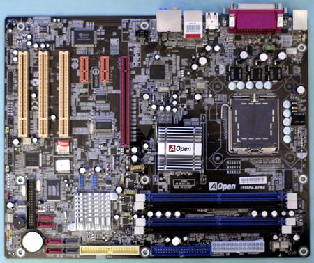
Recent AOpen boards have shown great attention to layout of the components and this is particularly true on the i915Pa. The nice-looking black board with rounded corners will look good in any case, and it will also be a great board for cable placements. The bulky connectors - 24-pin power, 12V 4-pin, IDE - are all at board edges where the bulky connectors can be kept out of the way. The only badly placed connector is the floppy, which won't matter to many, since they no longer use floppy drives. The CD-in connectors, for those who need them, are located above the slot area. This location is much easier to use than the afterthought location at the bottom of the board, which we have seen in some other designs. Front panel connections were also well-marked and easy to identify.
Most users will be pleased with the layout of the AOpen i915Pa. There is little to complain about and much to praise. Even the often overlooked fan connectors are here in numbers and locations to please most users.
AOpen i915Pa-EFRII: Overclocking and Stress Testing
FSB Overclocking Results
| Front Side Bus Overclocking Testbed | |
| Processor: | Pentium 4 Prescott LGA 775 560 ES (2.8GHz-3.6GHz) |
| CPU Voltage: | 1.425V (1.3675V default) |
| Cooling: | Thermaltake Jungle 502 |
| Power Supply: | OCZ Power Stream 520 |
| Maximum CPU OverClock: | 217x18 (3996MHz) +9% |
| Maximum FSB OC: | 217FSB x 14 (+9%) |
When the 915/925X boards first appeared, there was a lot of talk about a 10% overclock built into the 915/925X chipset. Manufacturers of boards that cater to enthusiasts, like Abit, Asus and DFI, quickly found ways to get around this design issue, but others did not seem to see this as a big problem. AOpen falls into the latter category here. Whether at stock multiplier or the Speedstep reduced 14X, the AOpen will reach 217 and nothing more.
Most users never overclock, and the AOpen is a great board for them, since it contains all the important performance features that are missing on many other 915 boards in the roundup. However, overclockers should look elsewhere for a 915 board as they will be very frustrated to be limited to a 9% overclock.
Memory Stress Test Results:
The memory stress test measures the ability of the AOpen i915Pa to operate at its officially supported memory frequency (533MHz DDR2), at the best performing memory timings that Crucial/Micron PC2-4300U will support. Memory stress testing was conducted by running DDR2 at 533MHz (stock 3:4 ratio) with 2 DIMM slots operating in Dual-Channel mode.| Stable DDR533 Timings - 2 DIMMs (2/4 DIMMs - 1 Dual-Channel Bank) |
|
| Clock Speed: | 266MHz |
| Timing Mode: | 3:4 (200:266 - Default) |
| CAS Latency: | 3.0 |
| Bank Interleave: | Auto |
| RAS to CAS Delay: | 3 |
| RAS Precharge: | 3 |
| Cycle Time (tRAS): | 10* |
| Command Rate: | N/A |
The AOpen i915Pa was completely stable with 2 DIMMs in Dual-Channel at the DDR2 settings of 3-3-3-10 at 1.8V default voltage. These are much faster settings than the DDR2 SPD and rated timings of 4-4-4-12.
Filling all four available memory slots is more strenuous on the memory subsystem than testing 2 DDR2 modules on a motherboard.
| Stable DDR533 Timings - 4 DIMMs (4/4 DIMMs - 2 Dual-Channel Banks) |
|
| Clock Speed: | 266MHz |
| Timing Mode: | 3:4 (200:266 - Default) |
| CAS Latency: | 4.0 |
| Bank Interleave: | Auto |
| RAS to CAS Delay: | 3 |
| RAS Precharge: | 3 |
| Cycle Time (tRAS): | 10 |
| Command Rate: | N/A |
DDR has a long benchmarking history that makes it easier to figure out where to go with memory timings. We are still in the learning curve with DDR2, and the old DDR patterns just do not work in DDR2. We found that no matter what the rest of the settings, 4 DIMMs with DDR2 generally required CAS 4 for stability. Timings like 3-4-3 or 3-4-4 appeared to work fine, and then we were suddenly facing hard drive corruption. Our advice for now is to use CAS 4 with 4 DIMMs for stability, although 4-3-3 timings did work fine on most of the test boards. If you plan on trying to raise voltage to attempt lower CAS with 4 DIMMs, then please backup your system first.
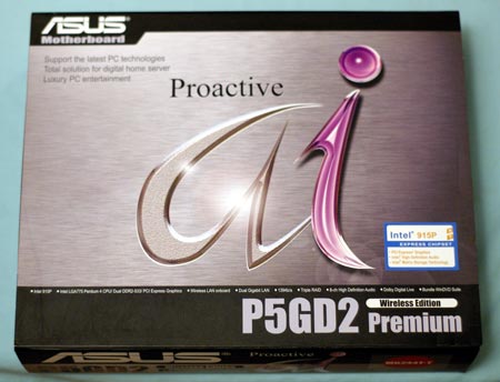
Asus P5GD2 Premium: Features and Layout
| Asus P5GD2 Premium Motherboard Specifications | |
| CPU Interface | Socket 775 Pentium 4 (Prescott) |
| Chipset | Intel 915P/ICH6R |
| BUS Speeds | 100MHz to 400MHz (in 1MHz increments) |
| DDR2 Speeds | Auto, 400, 533, 600 |
| PCI Speeds | To CPU, 33.33, Auto |
| Core Voltage | 1.4375V to 1.70V in 0.0125V increments |
| DRAM Voltage | Auto, 1.80V to 2.10V in 0.1V increments |
| Chipset Voltage | Auto, 1.5V, 1.6V |
| FSB Termination Voltage | Auto, 1.2V, 1.4V |
| Memory Slots | Four 240-pin DDR2 Slots Dual-Channel Unbuffered Memory to 4GB |
| Expansion Slots | 1 PCIe x16 Slot 2 PCIe x1 slot 2 PCI Slots |
| Onboard SATA/IDE RAID | 4 SATA 150 drives by ICH6R Can be combined in RAID 0,1,Intel Matrix plus 4 SATA 150 RAID by Sil3114R RAID 0, 1, 5, 10, JBOB(8 SATA Drives Total) /td> |
| Onboard IDE | One Standard ATA100/66 by ICH6R (2 100/66/33 drives) Plus 4 IDE by IT 8212F (4 133/100/66, RAID 0, 1, 0+1, JBOD) |
| Onboard USB 2.0/IEEE-1394 | 8 USB 2.0 ports 3 IEEE 1394b FireWire Ports by TI 1394b |
| Onboard LAN | 2 X Gigabit LAN Total 1 PCIe by Marvel 88E8052 1 PCI by Marvel 88E8001 |
| Onboard Audio | CMedia CMI9880 (Intel HD) 8-Channel with coaxial/optical SPDIF out Supports Dolby Digital Live |
| Wireless LAN | WiFi 802.11g Included |
| Tested BIOS | 1007 AMI |
Asus uses the Premium name for their flagship models. This makes the P5GD2 Premium the top 915 board from Asus. Asus offers many other 915 boards, depending on customer needs. Another particularly interesting 915 choice is the 915G-based P5GDC-V Deluxe, which uses either DDR or DDR2, offers both Integrated graphics and a PCIe x16 video slot, and still features an ICH6R south bridge.
The P5GD2 is based on the 915P north bridge and does feature add-on graphics only. The 915P was meant by Intel to cater to the more enthusiast-minded 915 buyers who would never even consider integrated graphics. In fact, the 915P and 915G are the same chipset, with the only difference being the integrated graphics of the 915G. All of the Asus Proactive AI (Artificial Intelligence) features are included on the Premium, and Asus proudly advertises the overclocking features. This includes a special cooling plate on the bottom of the board in the CPU area that Asus calls "Stack Cool".
While the Asus carries a very premium price tag also, there is certainly value here. Dual Gigabit LAN and 802.11g WiFi are included - with one gigabit LAN residing on the faster PCIe bus. You also get fast 1394B Firewire, premium HD audio with Dolby Digital Live, a total of 8 SATA ports and 6 IDE ports, overclocking features like stack cool, and RAID 5 and 10 options. As you will see in our overclocking tests, you also get the one of the best overclockers in the 915 universe.
You will also find the premium C-Media CMI9880 codec supporting the Intel High-Definition audio, with 8 channels and Dolby Digital Live technology support. The CMI9880 is the only audio solution in this roundup that has a built-in Dolby AC3 encoder, which can actually encode your digital audio into Dolby digital streams that can be output to the SPDIF for Dolby Digital playback. The CMI9880 does this real-time for any digital audio in your system to feed Dolby Digital playback. The rest of the boards in the roundup use sound solutions based on the newest HD codecs, but Asus carries High-Definition (Azalia) audio further on the P5GD2 Premium.
The storage area is another area where the Asus stands out. Several of the boards support the ICH6R standard 4SATA/1 IDE (2drives) configuration. The Asus adds 4 more SATA ports for a total of 8 SATA ports. The Asus goes even further by also adding 4 more IDE devices with the ITE controller for a total of 6.
If you can do without the high-speed Firewire (you still get 1394a), the 2nd Gigabit LAN (you still get PCIe Gigabit LAN), and a few other minor features (you still get 8 SATA and 6 IDE), you can save about $50 by buying the P5GD2 Deluxe. No one would ever call the Deluxe stripped in any way and it still isn't cheap, but it does provide a route to the P5GD2 with a little savings to boot.
The Asus P5AD2 Premium was our Gold Editor's Choice in the 925X Roundup, so there were high expectations for the Asus 915. We were not disappointed. The options and ranges available in the Asus BIOS are just as complete on the 915 board and they are truly useful for squeezing the most from the P5GD2. The one item that could use improvement, however, is the range of memory voltage controls. With competitors offering up to 2.5V on their 915 boards, the Asus seems a little short on memory voltage options. Other than that, the BIOS adjustments on the Asus are decent, and they also work. Some other boards in this roundup offer incredible FSB ranges that they could never reach with the other available options. They are more window dressing or bragging rights for reviews that just list ranges like checkmark features. The Asus tweak options, on the other hand, are useful and work to provide a great overclocking experience for users of the P5GD2.
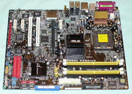
We have commented before that Asus pays close attention to the layout of their motherboards. We liked the layout of the P5AD2 Premium, and the P5GD2 Premium is mostly a P5AD2 with a 915P north bridge instead. The point is that we like the layout of the P5GD2. The floppy and 24-pin ATX are in the preferred upper right board-edge position, where they usually work best in most case designs. The 4-pin 12V connector is on the upper left board edge where it will not need to be snaked around the CPU and possibly, restrict air flow. The primary IDE is a right board-edge connector that should be preconnected during the install in tight cases. The 8 SATA ports are clustered at the lower right of the board (4 ports) and the bottom edge of the board (4 ports). The additional IDE connector is also near the bottom edge along with the headers for additional USB ports. IEEE1384b headers are between the PCIe x166 slot and the first regular PCI slot.
We were pleased that Asus had chosen to locate the Ahdio CD connector above the PCIe slot on this board. If you still need to use a CD audio cable, this is a much easier reach than the bottom of the board that Asus has used in the past.
The P5GD2 layout is close to ideal. You will likely be very pleased at the thought that went into the layout of the Asus motherboard.
Asus P5GD2 Premium: Overclocking and Stress Testing
FSB Overclocking Results
| Front Side Bus Overclocking Testbed | |
| Processor: | Pentium 4 Prescott LGA 775 560 ES (2.8GHz-3.6GHz) |
| CPU Voltage: | 1.425V (1.3875V default) |
| Cooling: | Thermaltake Jungle 502 |
| Power Supply: | OCZ Power Stream 520 |
| Maximum CPU OverClock: | 227x18 (4086MHz) +14% |
| Maximum FSB OC: | 279FSB x 14 (+40%) |
Asus has fully implemented Speedstep in their recent BIOS updates for the P5GD2 Premium, so the OC results are a lot more than academic - at least on this board. Speedstep means that the stock multiplier and a 14X multiplier will be available on all Prescott CPUs, opening new options for overclocking regular Intel Prescott chips.
You will also be extremely pleased with with the overclocking ability of the P5GD2. The stock multiplier overclock of 227x18 or 4086MHz is the highest frequency ever reached with this 3.6GHz Prescott. The 40% FSB overclock achieved at the 14X multiplier is also the highest OC that we have seen with a SATA drive on a Socket T board. Asus has implemented their magic in the Auto setting for PCI Express and this is the setting used for these overclocks. If you are interested in how Asus manages to reach such an outstanding overclock with the P5GD2, please check Breaking Intel's Overclock Lock: The REAL Story.
The fact that Asus manages a higher OC than more recognized OC boards like DFI and Abit is testament to the solid engineering that went into the P5GD2 design. Stack Cool and the other overclocking enhancements on the P5GD2 Premium apparently do a good job of extending the OC range on the Asus.
Memory Stress Test Results:
Memory stress tests look at the ability of the Asus P5GD2 premium to operate at the officially supported memory frequency (533MHz DDR2), at the best performing memory timings that Crucial/Micron PC2-4300U will support. Memory stress testing was conducted by running DDR2 at 533MHz (stock 3:4 ratio) with 2 DIMM slots operating in Dual-Channel mode.| Stable DDR533 Timings - 2 DIMMs (2/4 DIMMs - 1 Dual-Channel Bank) |
|
| Clock Speed: | 266MHz |
| Timing Mode: | 3:4 (200:266 - Default) |
| CAS Latency: | 3.0 |
| Bank Interleave: | Auto |
| RAS to CAS Delay: | 3 |
| RAS Precharge: | 3 |
| Cycle Time (tRAS): | 10* |
| Command Rate: | N/A |
The Asus P5GD2 Premium was completely stable with 2 DDR2 modules in Dual-Channel at the settings of 3-3-3-10 at 1.8V default voltage. This matches the best timings that all the motherboards in this roundup were able to achieve with DDR2 memory. 3-3-3 is also faster than the 4-4-4 timings specified for the Crucial/Micron DDR2 modules used for these benchmarks.
Filling all four available memory slots is more strenuous on the memory subsystem than testing 2 DDR2 modules on a motherboard.
| Stable DDR533 Timings - 4 DIMMs (4/4 DIMMs - 2 Dual-Channel Banks) |
|
| Clock Speed: | 266MHz |
| Timing Mode: | N/A |
| CAS Latency: | 4.0 |
| Bank Interleave: | N/A |
| RAS to CAS Delay: | 3.0 |
| RAS Precharge: | 10T* |
| Precharge Delay: | 3.0 |
| Command Rate: | N/A |
As we first saw on the Abit, 4 DDR2 DIMMs are not stable at CAS 3 as 2 DIMMs are. Once again, we required 4-3-3 timings when using 4 DDR2 DIMMs, though 4-3-3 worked fine at default voltage. Perhaps more voltage could improve stability at 3-3-3 with 4 DIMMs. We were able to achieve the stability at 2.0V (from default 1.8V) to complete Super Pi and Aquamark 3 at the 3-3-3 timings with 4 DIMMs.
Biostar P4TGP 775: Features and Layout
| Biostar P4TGP 775 Motherboard Specifications | |
| CPU Interface | Socket 775 Pentium 4 (Prescott) |
| Chipset | Intel 915P/ICH6R |
| BUS Speeds | 200MHz to 255MHz (in 1MHz increments) |
| DDR2 Speeds | Auto, 333, 400 |
| PCI Speeds | 33.33, 36.36, 40.00 |
| Core Voltage | 1.25V to 1.60V in 0.0125V increments |
| DRAM Voltage | Default, 1.86V, 1.9V |
| NB (Northbridge) Voltage | Default, 1.86V, 1.9V |
| Memory Slots | Four 184-pin DDR 400 Slots Dual-Channel Unbuffered Memory to 4GB |
| Expansion Slots | 1 PCIe x16 Slot 3 PCIe x1 slot 3 PCI Slots SLR (Biostar Home Gateway) Slot |
| Onboard SATA/RAID | 4 SATA 150 drives by ICH6R Can be combined in RAID 0, 1, Intel Matrix |
| Onboard IDE/RAID | One Standard ATA100/66 (2 drives) plus 4 33/66/100 Drives by ITE8212 (RAID 0, 1, 0+1) |
| Onboard USB 2.0/IEEE-1394 | 8 USB 2.0 ports 2 IEEE 1394a FireWire Ports by VIA VT6307 |
| Onboard LAN | Gigabit PCI Ethernet by Realtek 8110S 4-port Router Card for SLR slot (Included) |
| Onboard Audio | CMI9880 (HD Audio) 8-Channel with Dolby Digital DDICE |
| Tested BIOS | 1.0 Award |
Over the years, Biostar has developed a reputation for delivering very solid boards at very attractive prices. The P4TGP 7875 is a good example of the value that Biostar delivers. Based on the 915P chipset, the Biostar still uses the preferred solution of the the ICH6R for the south bridge. This gives users the option of using the standout features of Intel Matrix RAID if they choose. Biostar also didn't compromise on audio, providing a High Definition audio solution that operates at 192kHz with 24bits, a greater than 95db Signal-to-Noise Ratio and Dolby Digital interactive Content Encoder (DDICE) compliance.
We appreciate the thinking that must have gone into these decisions and we think that Biostar made the right decision including these two trademark 915/925X features. Biostar also provides Gigabit LAN, but there is the compromise here in that the LAN resides on the PCI bus instead of the faster PCI Express. Biostar also provides Firewire ports and corrects the oversight of just 2 IDE devices with an added 4 IDE devices (total 6) with the ITE8212 controller. If you have been actually checking specs in the roundup, you will find that these features are missing from many boards which sell in the price range of the Biostar.
The Biostar also comes with a very interesting and unique feature called an RC8650 Router Card, which fits in a special SLR slot on the P4TGP 775. Most people these days have a router in their home system, and it is interesting to see Biostar including a router as part of their motherboard package. The WAN LAN connector plugs in the top port in the slot and there are 3 additional network connections available for more systems. An on-board router is an interesting idea to differentiate your motherboard design.
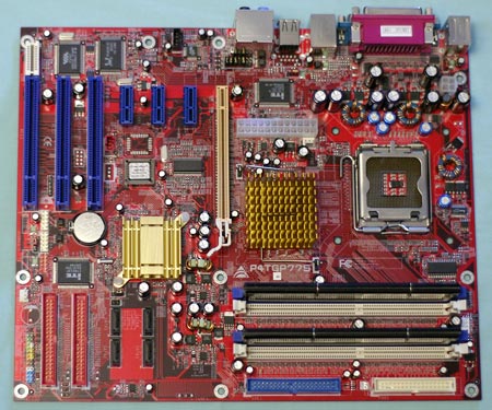
There is both good and bad in the Biostar P4TGP layout. Let's start with the good. The floppy and hard drive are in the preferred upper right edge location. This works best on most boards. The 4 SATA ports and 2 IDE connectors for 4 devices are also in reasonable locations at the lower right of the board. CD audio, if you need it, is around the midline of the board - in the PCIe slots area - which is OK. It would have been better above the slots. SPDIF in and out headers are in an unusual location between PCI2 x1 #3 and the first PCI slot. While the location looks a little strange, it works fine with accessory SPDIF brackets.
The most glaring fault in the Biostar layout, however, is a big one. The 24-pin ATX is in the middle of the board between the 915P north bridge and the rear IO. This is a horrible location that requires snaking the bulky 20/24-pin power cable around the CPU and hoping that it doesn't move and block air flow. The 12V 4-pin is better, near the top board edge, but the 20/24-pin really needs a new location on the Biostar board. Where other boards in the roundup seem to have some logic to their layout, the minor connectors on the Biostar seem to be sprinkled wherever there was room. The bulky cables except for power are OK, but things like the USB headers are in odd positions between slots.
We have complained in the past about boards where the memory slots are blocked by the video card. This is another board where you can't change memory without first removing the large video card. If you don't change memory very often, this will not be a problem, but if you frequently try out new memory, this tight fit will be a nuisance.
Overall, the decent layout of the rest of the bulky cables is marred by the horrible placement of the 20/24-pin power connector. Biostar would do themselves a favor by paying more attention to board layout in the future.
Biostar P4TGP 775: Overclocking and Stress Testing
FSB Overclocking Results
| Front Side Bus Overclocking Testbed | |
| Processor: | Pentium 4 Prescott LGA 775 560 ES (2.8GHz-3.6GHz) |
| CPU Voltage: | 1.425V (1.3875V default) |
| Cooling: | Thermaltake Jungle 502 |
| Power Supply: | OCZ Power Stream 520 |
| Maximum CPU OverClock: | 217x18 (3996MHz) +9% |
| Maximum FSB OC: | 217FSBx14 (+9%) |
Like a few other boards in the 915 roundup, Biostar has made no changes whatsoever to open up the stock 10% OC lock that we saw on the first 915/925X boards. It really doesn't matter whether you are trying to overclock at the stock 18X multiplier or a reduced 14X ratio - the limit is 217 FSB or about 9% overclock. If you are an overclocker or would like to try your hand at overclocking in the future, the Biostar is not a good choice. It is competitive at stock speeds and very stable at a small overclock, but this is not a board that will make an overclocker happy.
Memory Stress Test Results:
The Biostar uses DDR memory to ease the transition form a current platform to Socket T. The memory stress test measures the ability of the Biostar P4TGP 775 to operate at its officially supported memory frequency (DDR400), at the best performing memory timings that OCZ OC3200 Platinum Rev. 2 will support. Memory stress testing was conducted by running DDR400 at 1:1 ratio with 2 DIMM slots operating in Dual-Channel mode.| Stable DDR400 Timings - 2 DIMMs (2/4 DIMMs - 1 Dual-Channel Bank) |
|
| Clock Speed: | 200MHz |
| Timing Mode: | 1:1 (200:200 - Default) |
| CAS Latency: | 2.0 |
| Bank Interleave: | Auto |
| RAS to CAS Delay: | 2 |
| RAS Precharge: | 2 |
| Cycle Time (tRAS): | 5 |
The Biostar was completely stable with 2 DIMMs in Dual-Channel at the DDR timings of 2-2-2-10 at 2.6V default voltage.
Filling all four available memory slots is more strenuous on the memory subsystem than testing 2 DDR modules on a motherboard.
| Stable DDR400 Timings - 4 DIMMs (4/4 DIMMs - 2 Dual-Channel Banks) |
|
| Clock Speed: | 200MHz |
| Timing Mode: | 1:1 (200:200 - Default) |
| CAS Latency: | 2.0 |
| Bank Interleave: | Auto |
| RAS to CAS Delay: | 2 |
| RAS Precharge: | 2 |
| Cycle Time (tRAS): | 5 |
We often see boards from second tier manufacturers that have some issues when filling all memory slots on a motherboard. 4 DIMMs was not an issue for this Biostar as it handled 4 DS DIMMs at the same timings that had worked for 2 DIMMs. It appears that Biostar has paid careful attention to memory performance on the P4TGP 775 and the board performance is satisfying at stock speeds.
DFI LANParty UT 915P-T12: Features and Layout
DFI has implemented Intel Speedstep in their recent BIOS updates to the LANParty UT 915P-T12.| DFI LANParty UT 915P-T12 Motherboard Specifications | |
| CPU Interface | Socket 775 Pentium 4 (Prescott) |
| Chipset | Intel 915P/ICH6 |
| BUS Speeds | 200MHz to 380MHz (in 1MHz increments) |
| DDR2 Speeds | Auto, 400, 533 |
| PCI Speeds | To CPU, 33.33, Auto |
| PCI Express Speeds | Auto, Fix 100-140 |
| Core Voltage | 0.8375V to 1.95V in 0.0125V increments |
| DRAM Voltage | 1.8V to 2.5V in 0.1V increments |
| Northbridge Voltage | 1.5V to 1.8V in 0.1V increments |
| Memory Slots | Two 240-pin DDR2 Slots OR Two 184-pin DDR Slots (Can NOT be Used together) Dual-Channel Unbuffered Memory to 2GB |
| Expansion Slots | 1 PCIe x16 Slot 2 PCIe x1 slot 3 PCI Slots |
| Onboard SATA/IDE RAID | 4 SATA 150 drives by ICH6 |
| Onboard IDE | One Standard ATA100/66 (2 drives) |
| Onboard USB 2.0/IEEE-1394 | 8 USB 2.0 ports 2 IEEE 1394 FireWire Ports by VIA VT6307 |
| Onboard LAN | 2 Gigabit LAN - Marvel 88E8053 PCIe and Marvel 88E8001 PCI |
| Onboard Audio | Karajan Module with Realtek ALC880 Codec with Independent Variable Sampling 8-Channel with SPDIF in/out |
| Tested BIOS | Award 9/20/2004 |
When DFI introduced the LANParty boards in early 2003, they were not a name with which many Enthusiasts were familiar. However, since that time, DFI has earned a solid reputation as a maker of some of the best-performing and most sought-after boards available in the Enthusiast market. Where the LANParty name is used for the top performing boards produced by DFI geared for the enthusiast, the LANParty UT name has recently come into play to identify LANParty board designed for great value. The idea behind LANParty UT is to provide all of the overclocking finesse for which DFI is known, but also to deliver it with fewer features and fewer accessories included to keep the price more reasonable.

For example, you will not normally see front-panel break-out boxes and a PC Transpo harness included with a LANParty UT board, but you will normally see these features on a LANParty board. However, some things are still included in the package that you might not expect. Things like round IDE and Floppy cables in stand-out colors are still included.
The heart of any LANParty board is the performance and overclocking, and here, the options available for the enthusiast will keep most users very happy. First, the LANParty can use either DDR or DDR2 memory. This flexible arrangement allows you to carry some favorite DDR to the DFI board or to use the new DDR2 memory. Just keep in mind that you can't use both DDR and DDR2 together. The fact that you can use either, but not both memory, also limits the maximum memory usable on the UT 915P-T12.
DFI included some very high-end features that many enthusiasts will welcome. There are two Gigabit LAN ports - one based on the faster PCI Express bus and a standard Gigabit LAN that resides on the slower PCI bus. DFI also included a separate Karajan audio card for improved audio. The Karajan card isolates the High-Definition audio to improve signal-to-noise ratio, removing the biggest complaint of on-board audio, which is excessive noise. IEEE Firewire ports are also featured on the UT 915P-T12, though they are standard 1394a ports instead of the new and faster 1394b variety.
With all this attention to high-end features, you may well wonder what DFI left out. One significant omission is using the ICH6 south bridge instead of ICH6R. This will matter to some, since Intel Matrix RAID is not available, but others will say the RAID provides no real performance improvement anyway. The 2nd item is a larger surprise, however. DFI has just the one ICE port provided by the 915 chipset. This is a surprise, since the DFI reaches its highest overclock levels with IDE drives. With that being the case, it is really short-sighted to have to share an IDE drive and optical disks on a board supporting just two IDE devices. There are plenty of good performing SATA ports on the DFI, but to get to the screaming overclock stage, you will have to use IDE.
With a DFI LANParty - even the UT variety - you expect to get a wide range of overclocking controls and tweaks in the BIOS. Noteworthy on the 915P-T12 is a memory voltage range to default 1.8V to 2.5V and a similar set of DDR options to 3.2V. These are unusually wide for a motherboard and make it easier to squeeze the most performance form your memory. The CPU voltage extends all the way to 1.95V with a stock 1.3875V Prescott. This kind of range is frankly dangerous in the wrong hands, but it is high enough to satisfy mostly enthusiasts who will use water and phase-change cooling for their Prescott.
DFI also continues CMOS reloaded, which was introduced with the second generation LANParty and Infinity boards. This feature allows you to save several different custom BIOS setups, so you can easily recall custom BIOS settings for a particular overclock or settings for a different OS. Overclockers and users who run multiple operating systems will really find CMOS Reloaded to be a useful feature.
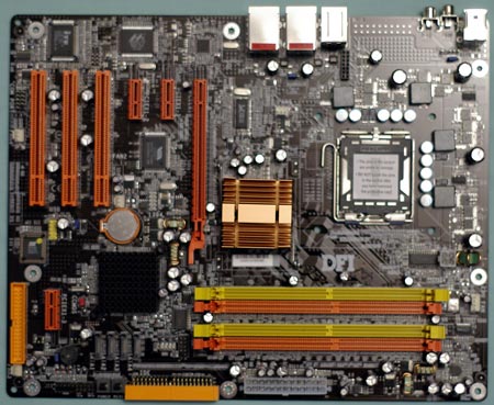
The DFI is very well laid out for most cases. The 20/24 ATX and 4-pin 12V are at board edge locations, and the single IDE is a midline board-edge connector that is best mounted before dropping the board in your case. Audio connectors like CD-IN are on the Karajan card. There are also momentary on/off and reset switches, a LANParty trademark feature on the right edge of the board. The only connector that is poorly located is the floppy connector at the bottom of the board. If you are one who still uses a floppy, this location will be a stretch - particularly in a full tower case that is likely to be used with a board such as the UT 915P-T12. While they don't stand out in the photo, DFI also includes 4 diagnostic LEDs on the board and a list of codes in the manual. They are not as easy to use as the 2-digit LEDs, but they still provide very useful info if you are having any issues with board
As we have come to expect with LANParty boards in all flavors, DFI continues to innovate with their LANParty line of boards. The LANParty UT is clearly aimed at the computer Enthusiast who cares most about pure performance. The UT boards look fine in side-window cases, but they are not as brash and showy as the regular LANParty series. The LANParty boards wouldn't sell unless they also delivered top-notch Enthusiast-level performance along with whatever else they bring to the table. Fortunately, DFI continues to lavish most of their attention on how the LANParty boards actually perform.
DFI LANParty UT 915P-T12: Overclocking and Stress Testing
FSB Overclocking Results
| Front Side Bus Overclocking Testbed | |
| Processor: | Pentium 4 Prescott LGA 775 560 ES (2.8GHz-3.6GHz) |
| CPU Voltage: | 1.425V (1.3875V default) |
| Cooling: | Thermaltake Jungle 502 |
| Power Supply: | OCZ Power Stream 520 |
| Maximum CPU OverClock: | 225 x 18 (4050MHz) +13% |
| Maximum FSB OC: | 273FSB x 14 (+37%) SATA |
Like Asus and Abit, DFI manipulates the PCIe frequency during boot to achieve higher overclocks. The DFI was able to reach a FSB of 273, a 37% FSB overclock, with an ATI X800 XT and SATA hard drive. This is the second highest overclock that we achieved with this hardware in the roundup and is very close to the results achieved with the Asus. Similarly, we reached 225x18 at the stock multiplier, which is close to the record set by the Asus P5AD2 Premium.
Since the issue was the SATA drive giving up at 273FSB, we also ran additional tests with the IDE hard drive - just to see where we could go on the DFI. With an IDE drive, we reached a setting of 302x14 (4.23GHz) at 1.5V before we ran out of CPU. Frankly, we needed much better cooling than we had at those overclock levels, so we made no attempt to run our benchmark suite on a machine at that overclock level. The LANParty UT 915P-T12 actually performed a bit better in our overclock tests than the big brother 925-T2 that we reviewed in our 925X roundup.
Memory Stress Test Results:
The memory stress test measures the ability of the DFI 915P-T12 to operate at its officially supported memory frequency (533MHz DDR2), at the best performing memory timings that Crucial/Micron PC2-4300U will support. The DFI supports both DDR and DDR2, like the Gigabyte Duo in this 915 roundup. However, all benchmarks and stress testing used DDR2 memory. The stress test was conducted running DDR2 at 533MHz (stock 3:4 ratio) with 2 DIMM slots operating in Dual-Channel mode.| Stable DDR533 Timings - 2 DIMMs (2/4 DIMMs - 1 Dual-Channel Bank) |
|
| Clock Speed: | 266MHz |
| Timing Mode: | 3:4 (200:266 - Default) |
| CAS Latency: | 3.0 |
| Bank Interleave: | Auto |
| RAS to CAS Delay: | 3 |
| RAS Precharge: | 3 |
| Cycle Time (tRAS): | 10* |
DFI performs without any problems at the best 3-3-3-10 DDR2 timings that worked well on other 915P boards which use DDR2 in this roundup. Since your memory choice is either DDR or DDR2 on the DFI, but not both, it is not possible to run more than 2 DIMMs in this dual channel board. Memory on the LANParty UT 915P-T12 is limited to the memory that can occupy 2 slots in Dual-Channel mode.
ECS PF4 915P Extreme: Features and Layout
| ECS PF4 915P Extreme Motherboard Specifications | |
| CPU Interface | Socket 775 Pentium 4 (Prescott) |
| Chipset | Intel 915P/ICH6 |
| BUS Speeds | 200MHz to 510MHz (in 1MHz increments) |
| DDR2 Speeds | Auto, 400, 533 |
| PCI Speeds | Asynch, Synch |
| Core Voltage | Auto, 1.125V to 1.5875V in .015V increments |
| DRAM Voltage | 1.8V to 2.2V in 0.1V increments |
| PCIe Voltage | 1.50V to 1.675V in .025V Increments |
| Memory Slots | Four 240-pin DDR2 Slots Dual-Channel Unbuffered Memory to 4GB |
| Expansion Slots | 1 PCIe x16 Slot 2 PCIe x1 Slots 3 PCI Slots |
| Onboard SATA/RAID | 4 SATA 150 drives by ICH6 Plus 2 SATA 150 by SiS 180 (SiS drives can be combined in RAID) |
| Onboard IDE/RAID | One Standard ATA100/66 (2 drives) Plus 2 Ultra ATA 133/100/66 By SiS 180 (SiS drives can be combined in RAID) |
| Onboard USB 2.0/IEEE-1394 | 8 USB 2.0 ports 2 IEEE 1394a FireWire Ports by VIA VT6307 |
| Dual Onboard LAN | Gigabit PCI Ethernet by Marvell 88E8001 10/100 PCI by Realtek 8100C |
| Onboard Audio | C-Media CMI9880 8-Channel with SPDIF |
| Tested BIOS | 1.1a AMI |
In the last year, ECS has been pushing for greater respect at the top end of the motherboard market with flashier designs and adjustment options associated with top-end boards aimed at the enthusiast. They call these boards their "Extreme Motherboards" and the PF4 915P is part of the new series. What makes the board Extreme? For starters, it is the packaging.
The PF4 915P comes in a foil box with an information flap, more like you would see with a Gigabyte board. Fortunately, ECS opted for a subdued blue, silver and black design that doesn't shout off the shelves. Inside the box is a very Abit-like group of fitted inside boxes for manuals and accessories. A very complete range of accessories is included. Particularly noteworthy are round black cables. Also included is a slot mount or 3-1/2 inch bay mount USB2/Firewire port bracket. This option is very clever and worth copying by other manufacturers. Despite the high-end image and packaging, ECS has priced the PF4 915P to compete with mainstream boards, as it is currently selling in the $120 to $130 price range in web stores.
The board itself is a soft medium purple with color used to locate most-used connectors easily. You can see the rounded corners, huge active Northbridge heatsink, and a Southbridge sink with fins that spell "EXTREME". ECS even includes a rear exhaust fan in the IO area to pull heat from the CPU area of the 4-phase design.
Layout of the PF4 915P is very clean. In addition to the huge standard list of 915P features, ECS adds a SiS 180 controller for 2 additional SATA ports and an added IDE connector. The SiS ports can be combined in RAID - a good thing, since ECS chose to use the ICH6 south bridge without RAID capabilities. Two Firewire ports are also provided for those who want on-board Firewire, and the Azalia high-definition 8-channel audio is driven by a C-Media codec.
Layout is better than average. Thankfully, the IDE and floppy connector are in our preferred right edge location, with the added IDE connector at the bottom edge. The 24-pin ATX power connector is also on the right edge, out of the way in most cases. The 4-pin connector, however, is near the center of the board between the CPU and rear IO ports, requiring the cable to be snaked around the CPU. We prefer a board-edge location, but the cable is actually easier to maneuver, since it has just 4 wires.
ECS makes quite a bit of noise about the Dual LAN capabilities of the PF4. Dual LAN is a nice feature, but in this case, one is Gigabit and one is 10/100. To make matters worse, both LANs are on the PCI bus. This is not an issue with the 10/100, but the Gigabit LAN would have been much more capable on the PCI Express bus.
All-in-all, there is little to complain about the layout or features provided on the ECS. It would have been nice to see an ICH6R instead and a PCIe Gigabit LAN, but these will only be important to some users. The BIOS options are certainly much more generous than what we are accustomed to seeing with ECS designs. ECS appears to have met their design goal of positioning the PF4 915P Extreme as a premium board with a nice mainstream price. If performance and overclocking match the layout and features, ECS will have a potent player in the market.
ECS PF4 915P Extreme: Overclocking and Stress Testing
FSB Overclocking Results
| Front Side Bus Overclocking Testbed | |
| Processor: | Pentium 4 Prescott LGA 775 560 ES (2.8GHz-3.6GHz) |
| CPU Voltage: | 1.425V (1.3875V default) |
| Cooling: | Thermaltake Jungle 502 |
| Power Supply: | OCZ Power Stream 520 |
| Maximum CPU OverClock: | 222x18 (3996MHz) +11% |
| Maximum FSB OC: | 237FSB x 14 (+19%) |
It appears that ECS has implemented some means of getting around the overclock limits of the 915/925X, since we were able to reach 237 x14, or 19%, on the 915P Extreme. We also reached 222, an 11% overclock, at the stock ratio of 18X. While this is not nearly as good as the 260 to 300 overclocks that we achieved with the Asus, DFI, and MSI, it is still a big improvement over the 217 limit seen on many of the 915P boards.
This overclock level on the ECS reminds us of some of the early BIOS efforts that floated PCIe at boot to achieve higher overclocks. Manufacturers did not really get much higher than this until they began floating the PCIe by a variable table at boot. Perhaps that means that ECS can achieve even better overclocks with a BIOS update in the future. For now, we were pleased to see worthwhile performance increases achieved by overclocking one of the best values you can find in a 915P motherboard.
Memory Stress Test Results:
The memory stress test measures the ability of the ECS PF4 915P Extreme to operate at its officially supported memory frequency (533MHz DDR2), at the best performing memory timings that Crucial/Micron PC2-4300U will support. Memory stress testing was conducted by running DDR2 at 533MHz (stock 3:4 ratio) with 2 DIMM slots operating in Dual-Channel mode.| Stable DDR533 Timings - 2 DIMMs (2/4 DIMMs - 1 Dual-Channel Bank) |
|
| Clock Speed: | 266MHz |
| Timing Mode: | 3:4 (200:266 - Default) |
| CAS Latency: | 3.0 |
| Bank Interleave: | Auto |
| RAS to CAS Delay: | 3 |
| RAS Precharge: | 3 |
| Cycle Time (tRAS): | 10* |
| Command Rate: | N/A |
The ECS performed as other boards in the 915 roundup did in being able to run with complete stability at 3-3-3-10 timings with two DDR2 DIMMs. The 915P Extreme was completely stable at these timings at the default 1.8V.
Filling all four available memory slots is more strenuous on the memory subsystem than testing 2 DDR2 modules on a motherboard.
| Stable DDR533 Timings - 4 DIMMs (4/4 DIMMs - 2 Dual-Channel Banks) |
|
| Clock Speed: | 266MHz |
| Timing Mode: | 3:4 (200:266 - Default) |
| CAS Latency: | 4.0 |
| Bank Interleave: | Auto |
| RAS to CAS Delay: | 3 |
| RAS Precharge: | 3 |
| Cycle Time (tRAS): | 10 |
| Command Rate: | N/A |
When all 4 DDR2 slots are filled, the ECS required slightly slower timings than with 2 DIMMs. As seen with many other 915 boards running DDR2 memory, CAS needed to be reduced to 4 for complete stability, although 4-3-3 timings were stable in our benchmarks with 4 DIMMs.
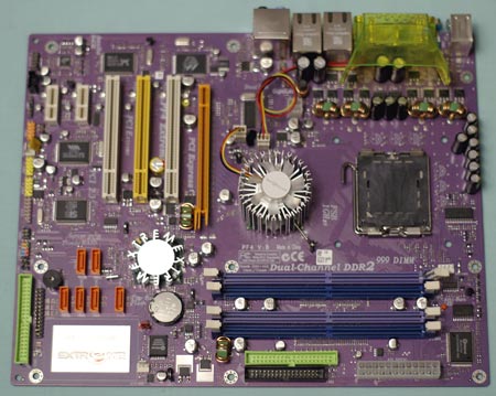
Epox 5epa+: Features and Layout
| Epox 5epa+ Motherboard Specifications | |
| CPU Interface | Socket 775 Pentium 4 (Prescott) |
| Chipset | Intel 915P/ICH6R |
| BUS Speeds | 100MHz to 400MHz (in 1MHz increments) |
| Realtime Turbo Mode | 202, 206, 210, 214, 220, 226 |
| DDR2 Speeds | Auto, 333, 400 |
| PCI Express Speeds | 100MHz to 150MHz in 1MHz increments |
| Core Voltage | -0.10V to +0.2125V in 0.0125V increments |
| DRAM Voltage | +0.1V to +0.7V in 0.1V increments |
| Memory Slots | Four 184-pin DDR Slots Dual-Channel Unbuffered Memory to 4GB |
| Expansion Slots | 1 PCIe x16 Slot 2 PCIe x1 slot 4 PCI Slots |
| Onboard SATA/RAID | 4 SATA 150 drives by ICH6R Can be combined in RAID 0, 1, Intel Matrix |
| Onboard IDE/RAID | One Standard ATA100/66 (2 drives) Plus 4 ATA133/100/66 drives by IT8212F ITE drives can be combined as RAID 0, 1, 0+1 |
| Onboard USB 2.0/IEEE-1394 | 8 USB 2.0 ports No FireWire Ports |
| Onboard LAN | Gigabit PCI Ethernet by Marvell 88E8001 |
| Onboard Audio | AC'97 2.3 Realtek ALC850 8-Channel with SPDIF |
| Tested BIOS | M265 |
Just before we completed the 915 roundup, Epox shipped us their newest version of the 5epa+ motherboard. Epox is well known for fast motherboards that overclock well, so we had high expectations of the performance of overclocking capabilities of this latest Epox board. The packaging is flashy with a large black package and standout graphics.
The Epox that we tested was the 5epa+ version, which included the RAID version of the ICH6R south bridge. While it was a pleasure to see ICH6R available as an option on the Epox 915, it was a disappointment to see some of the other choices that were made to keep prices down. First, the Intel High Definition audio has been replaced by an AC'97 2.3 Realtek ALD850. The 850 is a capable 8-channel audio codec, but it is certainly not the equivalent of Intel Azalia HD audio. We wish that Epox had found a way to keep HD audio like others here have done with boards that will sell in a similar price range. Next, Gigabit LAN is a nice feature, but this Gigabit LAN rides the slower PCI bus instead of the PCIe bus that could have provided better performance. When attached to PCI, there really isn't much advantage to Gigabit LAN over 10/100 LAN. Some will argue that none of us really need Gigabit LAN right now when broadband is hardly constrained by 100 LAN. However, if you need or want the advantages of Gigabit LAN, you won't find them on a Gigabit LAN saddled with the slower PCI bus. Last, there are no Firewire ports on the Epox. If you need them, look elsewhere, but for most, the missing Firewire ports really won't matter very much.
It is a good thing that Epox also noticed that 2 IDE devices would be very limiting for some users of the 5epa+. To correct this potential handicap, Epox added an ITE 8212 controller that provides support for four additional IDE devices.
Epox does not disappoint in the controls and ranges available for tweaking the 5epa+ in BIOS. The +0.7V maximum memory voltage translates into 3.3V from the stock 2.6V for the DDR memory supported by the Epox 915. This should be a range that will satisfy most memory overclockers. CPU voltage is also a generous range from a slight underclock (for cooler operation) to a +0.2125V overclock. This translates into 1.60V maximum with a current Prescott Socket T CPU.
When we first looked at the Epox, we recognized the unusual layout from our review of the Biostar P4TGP 775. The boards are not identical, features are a little different, but the 20/24-pin power connector is badly placed in the center of the board on both. Be careful when connecting the bulky power cable because it has to be routed around and behind the processor. The 12V 4-pin connector is better placed along the top edge of the board. All the IDE and floppy connectors, those driven by the chipset as well as those supported by the ITE controller, are located near the lower right edge of the board, below the midline. This is not a favorite location, but it still works fine with most board designs. With the diagnostic LEDs, SATA ports, and BIOS also located in this same area, it becomes a very busy quadrant. You need to plan cable routing to make sure that everything is still visible and/or accessible after the board is installed.
The 4 DIMM slots are also quite tight to the PCIe video slot plane. However, they are set further back than on most board designs, so they will only interfere with changing memory when you are using a very large video card.
Epox 5epa+: Overclocking and Stress Testing
FSB Overclocking Results
| Front Side Bus Overclocking Testbed | |
| Processor: | Pentium 4 Prescott LGA 775 560 ES (2.8GHz-3.6GHz) |
| CPU Voltage: | 1.425V (1.3875V default) |
| Cooling: | Thermaltake Jungle 502 |
| Power Supply: | OCZ Power Stream 520 |
| Maximum CPU OverClock: | 223x18 (4014MHz) +12% |
| Maximum FSB OC: | 254FSB x 14 (+27%) |
The 5epa+ is a better-than-average overclocker among 915 boards. It is not, however, the top level overclocker that we were hoping for. Above a 254 setting, SATA drives just disappeared, but the Epox continued to go through the pre-HD boot phase to 270 and even higher. This leads us to suspect that the Epox 5epa+ may actually reach even higher overclocks with IDE hard drives. At the stock 18x ratio, the Epox reached 4Ghz, but the CPU heatsink became quite hot in a very short time. For overclocks above around 3.9GHz, you really need better cooling with any of these 915 boards.
Manually selecting PCIe speeds had allowed us to reach higher overclocks on the MSI, so we tried the same technique on the Epox. We still couldn't break though 254 using SATA hard drives. It would be wrong to leave the impression that the highest FSB is a holy grail in our overclocking tests. To put the 254 FSB setting in perspective, this would represent DDR508 at a 1:1 memory ratio. This is an easily achieved overclock with fast memory timings and most current DDR400 memory based on Samsung TCCD chips. Some better TCCD memory on Brainpower DIMM PCBs can achieve DDR550 to DDR580 at reasonably fast timings. At 1:1 ratio, this would be a FSB setting of 275 to 290.
The question with overclocking is always where the trade off occurs. In this case, we have tested Crucial Ballistix DDR400 that does 2.5-2-2 at DDR500. So to run at DDR500 at the fastest speed that our CPU can achieve (about 4Ghz), we would need to run at 250 x16. We can actually run those settings with the unlocked ES 3.6GHz Prescott, but current Intel Socket T (775) processors can run at default ratio or 14X.
Memory Stress Test Results:
The Epox 5epa+ was designed to run DDR400 memory. The memory stress test measures the ability of the 5epa+ to operate at its officially supported memory frequency (DDR400), at the best performing memory timings that OCZ PC3200 Platinum Rev. 2 will support. Memory stress testing was conducted by running DDR at 400MHz (stock 1:1 ratio) with 2 DIMM slots operating in Dual-Channel mode.| Stable DDR400 Timings - 2 DIMMs (2/4 DIMMs - 1 Dual-Channel Bank) |
|
| Clock Speed: | 200MHz |
| Timing Mode: | 1:1 (200:200 - Default) |
| CAS Latency: | 2.0 |
| Bank Interleave: | Auto |
| RAS to CAS Delay: | 2 |
| RAS Precharge: | 2 |
| Cycle Time (tRAS): | 5 |
The Epox ran a single dual-channel (2 DIMMs) at the most aggressive 2-2-2-5 timings at default voltage. The 5epa+ was completely stable at these timings at the default 2.6V.
Filling all four available memory slots is more strenuous on the memory subsystem than testing 2 DDR modules on a motherboard.
| Stable DDR400 Timings - 4 DIMMs (4/4 DIMMs - 2 Dual-Channel Banks) |
|
| Clock Speed: | 200MHz |
| Timing Mode: | 1:1 (200:200 - Default) |
| CAS Latency: | 2.0 |
| Bank Interleave: | Auto |
| RAS to CAS Delay: | 2 |
| RAS Precharge: | 2 |
| Cycle Time (tRAS): | 5 |
When all 4 DDR slots are filled, the Epox matched the performance of the top DDR boards in the roundup, running with stability at the same 2-2-5 timings that worked well with 2 DIMMs.
Foxconn 915A01-P-8EKRS: Features and Layout
| Foxconn 915A01 Motherboard Specifications | |
| CPU Interface | Socket 775 Pentium 4 (Prescott) |
| Chipset | Intel 915P/ICH6R |
| BUS Speeds | 200MHz to 350MHz (in 1MHz increments) |
| DDR2 Speeds | Auto, 400, 533 |
| PCI Speeds | 33.33, 36.36, 40.00, Ref PCIex |
| PCI Express Speeds | 100MHz to 200MHz in 1MHz increments |
| Core Voltage | -0.025V to +0.10V in 0.0125V increments |
| DRAM Voltage | NO Options |
| Memory Slots | Four 240-pin DDR2 Slots Dual-Channel Unbuffered Memory to 4GB |
| Expansion Slots | 1 PCIe x16 Slot 3 PCIe x1 slot 3 PCI Slots |
| Onboard SATA/RAID | 4 SATA 150 drives by ICH6R Can be combined in RAID 0, 1, Intel Matrix |
| Onboard IDE | One Standard ATA100/66 (2 drives) |
| Onboard USB 2.0/IEEE-1394 | 8 USB 2.0 ports 2 IEEE 1394a FireWire Ports by VIA VT6307 |
| Onboard LAN | Gigabit PCI Ethernet by Realtek 8110S-32 |
| Onboard Audio | Realtek ALC880 (HD Audio) 8-Channel with SPDIF |
| Tested BIOS | 915A03G Award 10/28/2004 |
The Foxconn 925A01, tested in the 925X roundup, was the first full-featured Foxconn board that we had tested. The 915A01 continues in that same vein as a full-featured Socket 775 motherboard based on the Intel 915P chipset. Foxconn has earned a reputation of building solid motherboards that represent very good value. The Foxconn 915A01 fits that market segment better than the premium 925X board that we reviewed, since Intel considers the 915 to be the mainstream version of their Socket 775 chipsets. Almost everyone offers a 915 "mainstream" motherboard, so Foxconn can carve out a value niche for their boards in this segment.
When we take a closer look at the 915A01, we see that Foxconn can manufacture it in many flavors. The numbers at the end of the board name represent available options that are on the board. In the case of the test board, it is 8EKRS. A quick check of the Foxconn manual shows that this board adds to the base model: 8-channel HD audio, firewire, 1G LAN, and SATA RAID. With these exact same features, you will find this Foxconn 915 selling for around $150 at online retailers.
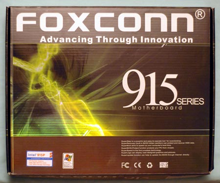
While we can attest to the solid and reliable operation of Foxconn boards, we have been very surprised that Foxconn has had so much difficulty building a competitive enthusiast grade board. Every time that we test a Foxconn board, a BIOS seems to come later that adds any overclocking options at all, and the boards always seem to be missing the most important adjustments for memory voltage. It's really a shame that Foxconn can't get this right because when you can buy a DFI for $160, an Albatron 915P Pro for $109, or an Abit AG8 for $128, then the question is, why would you buy a Foxconn for $150 and it doesn't even have any adjustments for memory voltage?
It is good to see Foxconn offering the most important options from the 915 options. High-Definition audio and the ICH6R chipset with Intel Matrix RAID are both a part of the 915A01 board that we are testing. So is Gigabit LAN, but it is (once again) the slow PCI version instead of the faster PCIe LAN chip. Other than the complaint about PCI LAN, the feature set of the 915A01 is just fine, and the feature list will satisfy most users. Foxconn even includes the 6 mini-jacks needed for Intel High Definition audio, and Firewire ports for those who prefer that interface. The only weakness in the audio ports is that only an SPDIF coaxial connector is provided on an accessory bracket. There is no provision at all for an optical connector.
The Foxconn is not quite up to the level of the top 50% of boards in this roundup, but it is close. The 915A01 is rock solid no matter what we threw at it, and it only seems less than capable when we looked at the much abbreviated options for tweaking to get the best performance and overclocking on the board.
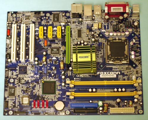
Layout of the Foxconn 915A01 is very good - much better than you might expect. Floppy and IDE connectors are located at the preferred upper right board edge. So is the 24/20-pin power connector. The 12V requires fishing the cable around the CPU, but this is an issue with many 915 boards anyway. It would be better if this 4-pin connector was also at a board edge.
There is one annoying item on every Foxconn board that we have reviewed so far, and that is the front panel connections. Foxconn seems to like the connections, which includes a 9-pin USB-like arrangement with no color-coding or other means to identify the panel connector. As a result, every time that we connect a Foxconn board, one of the connectors is usually set up wrong. It is also a fact that every case that we have in the lab has a 3-pin power LED connector, with just one exception. In the Foxconn universe, however, all power LEDs are 2-pin. We have seen a number of boards with a preference for 2-pin power LED connections, but most provided a 3-pin option also. It would be really appreciated if Foxconn would consider the same Power LED option on their boards. For those of you with a 3-pin power LED, the only option on the Foxconn is to modify your cable or leave the power LED disconnected.
Nitpicks aside, the Foxconn really has little to complain about in board layout. We mounted all of the boards in the roundup in a typical mid-tower case just to see how the layout worked and the Foxconn was an easier layout to work with than most.
Foxconn 915A01: Overclocking and Stress Testing
FSB Overclocking Results
| Front Side Bus Overclocking Testbed | |
| Processor: | Pentium 4 Prescott LGA 775 560 ES (2.8GHz-3.6GHz) |
| CPU Voltage: | 1.425V (1.3875V default) |
| Cooling: | Thermaltake Jungle 502 |
| Power Supply: | OCZ Power Stream 520 |
| Maximum CPU OverClock: | 216x18 (3888MHz) +8% |
| Maximum FSB OC: | 216FSB x 14 (+8%) |
The whole reason for FSB and voltage adjustments is what they can actually do for the board's performance. As you can see, Foxconn has made no efforts at all to provide overclocking above and beyond the 10% level. In fact, the best that we could do at any ratio was an 8% OC to 216. This is the worst overclocking performance of any 915 board in the roundup. The Foxconn is a decent performer at stock speeds, but if you are looking for a 915 overclocking solution, you really need to look elsewhere or learn a great deal about using PCI speed adjustments to reach higher overclocks.
Memory Stress Test Results:
The memory stress test measures the ability of the Foxconn 915A01 to operate at its officially supported memory frequency of DDR2-533, at the best performing memory timings that Crucial/Micron PC2-4300U will support. Memory stress testing was conducted by running DDR2 at 533MHz (stock 3:4 ratio) with 2 DIMM slots operating in Dual-Channel mode.| Stable DDR533 Timings - 2 DIMMs (2/4 DIMMs - 1 Dual-Channel Bank) |
|
| Clock Speed: | 266MHz |
| Timing Mode: | 3:4 (200:266 - Default) |
| CAS Latency: | 3.0 |
| Bank Interleave: | Auto |
| RAS to CAS Delay: | 3 |
| RAS Precharge: | 3 |
| Cycle Time (tRAS): | 10* |
The Foxconn matched the other boards in the 915 roundup in being able to run with complete stability at 3-3-3-10 timings with two DDR2 DIMMs. The 915A01 was completely stable at these timings at the default 1.8V.
Filling all four available memory slots is more strenuous on the memory subsystem than testing 2 DDR2 modules on a motherboard.
| Stable DDR533 Timings - 4 DIMMs (4/4 DIMMs - 2 Dual-Channel Banks) |
|
| Clock Speed: | 266MHz |
| Timing Mode: | 3:4 (200:266 - Default) |
| CAS Latency: | 4.0 |
| Bank Interleave: | Auto |
| RAS to CAS Delay: | 4 |
| RAS Precharge: | 3 |
| Cycle Time (tRAS): | 10 |
| Command Rate: | N/A |
When all 4 DDR2 slots are filled, the Foxconn required slightly slower timings than the top boards in the roundup, requiring 4-4-3 timings for complete stability instead of the 4-3-3, which worked well on most 915 boards. This is the same memory pattern seen with the 925X Foxconn board when we tested that board.
Gigabyte 8GPNXP Duo: Features and Layout
| Gigabyte 8GNXP Duo Motherboard Specifications | |
| CPU Interface | Socket 775 Pentium 4 (Prescott) |
| Chipset | Intel 915P/ICH6R |
| BUS Speeds | 100MHz to 600MHz (in 1MHz increments) |
| DDR2 Speeds | Auto, 1.66, 2.00, 2.66 |
| PCI Express Speeds | Asynch, Synch |
| vCore Voltage | 0.8375V to 1.60V in 0.0125V increments |
| DRAM Voltage | Normal, +.1, +.2, +.3 |
| PCI Express Voltage | Normal, +.1, +.2, +.3 |
| Memory Slots | Two 240-pin DDR2 Slots Plus four 184-pin DDR400 Slots Dual-Channel Unbuffered Memory to 4GB |
| Expansion Slots | 1 PCIe x16 Slot 3 PCIe x1 slot 2 PCI Slots |
| Onboard SATA/RAID | 4 SATA 150 drives by ICH6R Can be combined in RAID 0, 1, Intel Matrix |
| Onboard IDE/RAID | One Standard ATA100/66 (2 drives) Plus 4 drives by ITE 8212 (RAID 0, 1, 0+1) |
| Onboard USB 2.0/IEEE-1394 | 8 USB 2.0 ports 3 IEEE 1394b FireWire Ports by TSB81BA3 |
| CIA2 Motherboard Accelerator | Disabled, Cruise, Sports, Racing, Turbo, FullThrust |
| Onboard LAN | PCIe Gigabit LAN by Broadcom PLUS 5751Gigabit PCI Ethernet by Marvel 8001 |
| Onboard Audio | C-Media ALC880 (HD Audio) 8-Channel with SPDIF in/out |
| Wireless LAN | WiFi 802.11g Included |
| Tested BIOS | F5 Award |
The Gigabyte 8GPNXP-Duo, like the DFI LANParty UT 915P-T12, is designed to make the upgrade path to Socket 775 as easy and flexible as possible. Both boards will work with DDR2 or DDR memory. The Gigabyte adds a further twist by providing 4 DIMM slots for regular DDR memory. Gigabyte includes their trademark Dual-Power module to provide 8-phase power to the 8GPNXP-D. Gigabyte has redesigned the Dual-Power module for their latest Intel Socket T boards. It is lower profile and is located between the ports and the CPU where it will not interfere with airflow to/from the CPU. More than any other manufacturer, Gigabyte tends to load their top motherboards with every feature but the kitchen sink, and in this regard, the 8GNXP-Duo is a loaded motherboard even though it is based on the mainstream 915P.
We first tested the 8GPNXP-Duo in our launch review of the 915/925X chipset, where it was very useful to have a board supporting both DDR and DDR2 for our testing. In this 915 roundup, we have tested both dual memory motherboards with DDR2 memory, since we have found DDR2-533 running at more aggressive 3-3-3-10 timings to be a small amount faster than DDR.
Features of the 8GPNXP-Duo are very similar to the Gigabyte 8ANXP-D motherboard tested in the 925X roundup. This includes Dual Gigabit LAN connections with the Broadcom attached to the faster PCI Express bus and the Marvel attached to the PCI bus. Gigabyte provides 4 SATA ports with RAID capabilities supported by ICH6R. 4 more IDE ports are added to the ICH6R 2 ports (total 6) with the added ITE 8212 controller. Since many have complained about just 2 IDE ports on the 915/925X chipset, buyers of the Gigabyte will appreciate the additional ports for IDE (PATA) devices.
Gigabyte was the first manufacturer to support on-board fast Firewire "b" ports and 3 1394B ports are included on the 8GNXP-Duo. Gigabyte also fully supports the Realtek ALC880 high-definition audio codec, which interfaces with the Intel HD audio (Azalia).
A wide range of overclocking options is available in BIOS with useful ranges for the typical overclocker. Memory voltage can be adjusted to 2.1V from 1.8V, a wider range than Gigabyte usually provides for memory. The FSB, CPU voltage, and PCI Express voltage also have ranges that are useful for overclockers. Gigabyte does not provide any BIOS options for PCI Express clocks, so you have to depend on the board to make adjustments for you to get past the 10% overclock roadblock.
Layout of the Gigabyte generally works well, and we do like the pull release for the PCIe x16 slot. All you have to do is mount and unmount a 2-slot nVidia 6800 Ultra to learn to hate the push-lever design used on most motherboards. There are a couple of things that could definitely be improved upon on the layout of the Gigabyte, however, and they are the same complaints voiced in the Gigabyte 8ANXP-D The IDE and floppy connectors are at the end of the PCIe video slot - a terrible location. What makes it worse is a long card (like the nVidia 6 series) falls right between the floppy and IDE connector, making cable routing to mount and unmount the video card to be a real pain. The 24-pin power connector is fine at the upper right edge, but the 4-pin 12 volt sits almost in the center left of the board. That makes snaking the 12V cable around the CPU difficult in most case designs. The 4-pin 12V connector would be better located at the board edge where it would not interfere with the heatsink/fan on the CPU. You can work around these two issues, but they can definitely be improved upon. Otherwise, the layout works fine in most cases.
Gigabyte 8GPNXP Duo: Overclocking and Stress Testing
FSB Overclocking Results
| Front Side Bus Overclocking Testbed | |
| Processor: | Pentium 4 Prescott LGA 775 560 ES (2.8GHz-3.6GHz) |
| CPU Voltage: | 1.425V (1.3875V default) |
| Cooling: | Thermaltake Jungle 502 |
| Power Supply: | OCZ Power Stream 520 |
| Maximum CPU OverClock: | 218x18 (3996MHz) +9%/td> |
| Maximum FSB OC: | 218FSBx14 (+9%) |
With the recent introduction of Intel Speedstep, overclocking an Intel 775 CPU can be done by raising the FSB at the stock multiplier or by lowering the CPU to 14X ratio and then raising the FSB more. Therefore, we ran all OC tests at the stock ratio and at the 14X Speedstep ratio. The ratio really didn't matter on the 8GPNXP-Duo as we could only reach 218 at any ratio. It appears that Gigabyte has more work to do on the 8GPnXP-Duo to get around the 10% OC lock. Since Gigabyte managed this task on the sister 915X chipset 8ANXP-D, this may still be possible with BIOS updates.
Memory Stress Test Results:
The Gigabyte can use either DDR or DDR2 memory. Benchmarks were run with DDR2 memory and a memory stress test was run to measure the ability of the Gigabyte 8GPNXP-D to operate at its officially supported memory frequency (533MHz DDR2), at the best performing memory timings that Crucial/Micron PC2-4300U will support. Memory stress testing was conducted by running DDR2 at 533MHz (stock 3:4 ratio) with 2 DIMM slots operating in Dual-Channel mode.| Stable DDR533 Timings - 2 DIMMs (2/4 DIMMs - 1 Dual-Channel Bank) |
|
| Clock Speed: | 266MHz |
| Timing Mode: | 3:4 (200:266 - Default) |
| CAS Latency: | 3.0 |
| Bank Interleave: | Auto |
| RAS to CAS Delay: | 3 |
| RAS Precharge: | 3 |
| Cycle Time (tRAS): | 10* |
| Command Rate: | N/A |
Like the other motherboards in this 915 roundup, the Gigabyte was completely stable with 2 DDR2 modules at the best performing settings of 3-3-3-10 at default speed and 1.8V default voltage.
Since the Gigabye can run either DDR or DDR2, but not both simultaneously, we could not test with 4 DDR2 DIMMs.
Jetway 915 PDBG: Features and Layout
| Jetway 915 PDBG Motherboard Specifications | |
| CPU Interface | Socket 775 Pentium 4 (Prescott) |
| Chipset | Intel 915P/ICH |
| BUS Speeds | 200MHz to 255MHz (in 1MHz increments) |
| DDR Speeds | Auto, 333, 400 |
| Core Voltage | 0.8375V to 1.60V in 0.0125V increments |
| DRAM Voltage | 1.80V to 2.25V in 0.05V increments |
| VDD 1.5 Voltage | 1.50V-2.0V in 0.05V increments |
| Memory Slots | Four 184-pin DDR400 Slots Dual-Channel Unbuffered Memory to 4GB |
| Expansion Slots | 1 PCIe x16 Slot 2 PCIe x1 slot 4 PCI Slots |
| Onboard SATA/RAID | 4 SATA 150 drives by ICH6 Plus 2 SATA drives by SiS180 (0, 1, 0+1) |
| Onboard IDE/RAID | One Standard ATA100/66 (2 drives) Plus 2 drives by SiS 180 (0, 1, 0+1) |
| Onboard USB 2.0/IEEE-1394 | 8 USB 2.0 ports 2 IEEE 1394 FireWire Ports by VIA VT6307S |
| Onboard LAN | Gigabit PCI Ethernet by Realtek 8100S |
| Onboard Audio | Realtek ALC880 (HD Audio) 8-Channel with SPDIF in/out |
| Tested BIOS | Award 7/07/2004 |
Jetway supplied early versions of both their 915P and 915G motherboards. The boards are the same except for the integrated Intel DX9 graphics capabilities of the G chipset. While the 915 is the "mainstream" chip in the new Socket 775 chipsets, Jetway did not short-change the features on their 915PDBG board. Included are the trademark High-Definition audio powered by the Realtek ALC880, 2 VIA Firewire ports, and Gigabit LAN running on the slower PCI bus. The Gigabit LAN would have performed better on the faster PCIe bus, but in most real applications today, you won't really notice the difference.
Jetway economized by using the ICH6 south bridge instead of the R version that supports Intel Matrix RAID. Then they added A SiS 180 controller to provide 2 needed IDE ports (total 4) to the 915 chipset and 2 more SATA ports (total 6). The added drives on the SiS 180 controller can be combined in RAID arrays if the user chooses.
The BIOS options and ranges of the Jetway 915PDGB are surprisingly complete. Memory Voltage, CPU Voltage and VDD (Chipset) voltage all have wide and useful ranges. The only BIOS adjustment that could use a boost in BIOS upgrade is the FSB adjustment, which is currently limited to a pretty low 255 setting. Jetway designed the 915P.R boards to use DDR memory to lower the cost of an upgrade to the new Socket T platform.
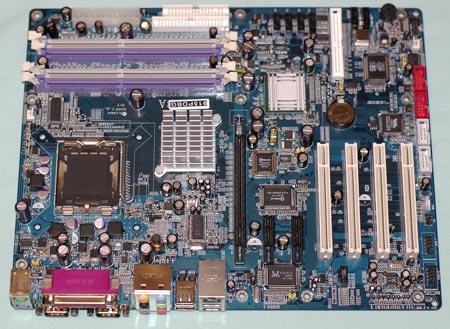
Jetway did a fine job in the layout of the 915PBDG. The board is a decidedly non-flashy standard green with rounded corners, but the components and connectors are in locations where they make sense. The floppy and IDE connector supported by the ICH6 are in the best location at the upper right board edge, between the memory slots and the board edge. The 24/20-pin power connector is in the same area where it belongs. While the 4-pin 12V power connector is between the CPU socket and the IO ports, it completely clears the CPU area at least, making it easier to connect and route around the CPU heatsink/fan. The 6 SATA connectors and onboard headers for features are all along board edges where they belong. It is also worth noting that the SATA connectors are the completely enclosed type, which makes the fragile SATA connector much more durable for day-in/day-out service.
We don't know if the Jetway 915PBDG will ever see the light of day in most world markets. As Anand discussed after his recent visit to Taiwan, manufacturers are extremely disappointed with the very slow sales of 915/925X boards. With supplies of 865/875 drying up, there may be a corresponding boost in 915/925X sales. If there is a boost in 915 demand, then look for the Jetway in the market. The design of the board is very good and Jetway could have a winner here with some refinement - if the market wants a 915P board.
Jetway 915 PDBG: Overclocking and Stress Testing
FSB Overclocking Results
| Front Side Bus Overclocking Testbed | |
| Processor: | Pentium 4 Prescott LGA 775 560 ES (2.8GHz-3.6GHz) |
| CPU Voltage: | 1.425V (1.3875V default) |
| Cooling: | Thermaltake Jungle 502 |
| Power Supply: | OCZ Power Stream 520 |
| Maximum CPU OverClock: | 214x18 (3852MHz) +7% |
| Maximum FSB OC: | 216FSB x 16 (+8%) |
While the Jetway is a decent performer at stock speeds, the overclocking performance is pretty dismal. The options are there for this board to be a good overclocking performer, but it appears that Jetway has done little with the 915 design, since the demand has been so low in the market. We hope that if Jetway decides to bring the 915PDBG to market, they will update the BIOS to improve overclocking performance significantly.
Memory Stress Test Results:
Jetway designed the 915GDBG and 915PDGB to use DDR memory. Memory stress tests therefore measured the ability of the Jetway to operate at its officially supported memory frequency of DDR400, at the best performing memory timings that our standard OCZ PC3200 Platinum Rev. 2 will support. Memory stress testing was conducted by running DDR400 at a stock 1:1 ratio with 2 DIMM slots operating in Dual-Channel mode.| Stable DDR400 Timings - 2 DIMMs (2/4 DIMMs - 1 Dual-Channel Bank) |
|
| Clock Speed: | 200MHz |
| Timing Mode: | 1:1 (200:200 - Default) |
| CAS Latency: | 2.0 |
| Bank Interleave: | Auto |
| RAS to CAS Delay: | 2 |
| RAS Precharge: | 2 |
| Cycle Time (tRAS): | 5 |
The Jetway 915PDBG was completely stable with 2 DIMMs in Dual-Channel at the DDR400 and memory timings of 2-2-2-5 at 2.6V default voltage.
Filling all four available memory slots is more strenuous on the memory subsystem than testing 2 DDR2 modules on a motherboard.
| Stable DDR400 Timings - 4 DIMMs (4/4 DIMMs - 2 Dual-Channel Banks) |
|
| Clock Speed: | 200MHz |
| Timing Mode: | 1:1 (200:200 - Default) |
| CAS Latency: | 2.0 |
| Bank Interleave: | Auto |
| RAS to CAS Delay: | 3 |
| RAS Precharge: | 2 |
| Cycle Time (tRAS): | 5 |
DDR has a long benchmarking history that makes it easier to figure out where to go with memory timings. We found that the RAS-to-CAS delay needed to be increased to a 3 setting for complete stability with 4 DIMMs in the Jetway. 4 DIMMs were completely stable at 2-3-2-5 settings at a default 2.6V memory voltage.
MSI 915P Neo2 Platinum: Features and Layout
| MSI 915P Neo2 Platinum Motherboard Specifications | |
| CPU Interface | Socket 775 Pentium 4 (Prescott) |
| Chipset | Intel 915P/ICH6R |
| BUS Speeds | 100MHz to 400MHz (in 1MHz increments) |
| DDR2 Speeds | Auto, 400, 533, 600, 667, 700, 710 |
| PCI Speeds | 33.3, 36.3, 40.0 |
| Core Voltage | CPU Default to 1.55V in 0.0125V increments |
| DRAM Voltage | 1.80V to 2.4V in 0.05V increments |
| NB (Northbridge) Voltage | 1.50V-2.05V in 0.05V increments |
| Memory Slots | Four 240-pin DDR2 533 Slots Dual-Channel Unbuffered Memory to 4GB |
| Expansion Slots | 1 PCIe x16 Slot 2 PCIe x1 slot 3 PCI Slots |
| Onboard SATA/RAID | 4 SATA 150 drives by ICH6R Can be combined in RAID 0,1,Intel Matrix |
| Onboard IDE/RAID | One Standard ATA100/66 (2 drives) Plus 4 drives by VIA VT6410 - Drives can be combined as RAID 0, 1, 0+1 |
| Onboard USB 2.0/IEEE-1394 | 8 USB 2.0 ports 3 IEEE 1394 FireWire Ports by VIA VT6306 |
| Onboard LAN | Gigabit PCIe Ethernet by Broadcomm BCM5751 |
| Onboard Audio | CMI9880L (HD Audio) 8-Channel with SPDIF in/out |
| Tested BIOS | 1.5 AMI |
MSI was surprisingly absent from our earlier roundup of 925X motherboards. This was quite a surprise, since MSI was the only Tier 1 (major) motherboard maker without a product in the 925X roundup. The issue was not that MSI would not make a 925X board, but rather that MSI had many 925X/915 boards in their early production with bad ICH6 family south bridges. MSI decided to hold back shipping any 915/925X products until they could retest and certify products as built with south bridges that performed as they should.
Now, as we are testing for the 915 roundup, MSI has provided their MSI 915P Neo2 Platinum for review. If the name sounds familiar, it is because the MSI K8N Neo2 Platinum is one of the best known and top-performing AMD Socket 939 motherboards. MSI apparently uses the Neo2 Platinum name a lot - to designate their top boards in any given family.
The MSI 915P Neo2 Platinum will be immediately recognizable to owners of other Neo and Neo2 products. Call it the family resemblance because the packaging for all the Neo2 boards is very similar.
Like Asus, MSI puts the right ingredients into the mix for their 915P board. This includes using the ICH6R south bridge to provide Intel Matrix RAIS capabilities, the C-Media High Definition audio, the use of Gigabit LAN that resides on the higher speed PCIe bus, or the excellent addition of 4 more IDE ports to supplement the "just 2" provided by the ICH6R south bridge. When we talk about the right mix of 915 features, it could almost be a specification list for MSI or Asus. In this roundup, we at least agree with what the major players believe is important in a 915 design. That has rarely been the case in the past.
MSI also distinguishes itself with excellent tweak/OC options in their AMI BIOS. Memory voltage can be adjusted to an outstanding 2.4V from the stock 1.8V. Northbridge voltage can be adjusted over a similarly broad range. The CPU voltage adjustment range seems more restricted, but a range to 1.55V with a CPU rated at 1.385V does provide some adjustment range. Water and phase-change cooling advocates will wish for a bit more CPU voltage range though. The CPU FSB range from 200 to 500 is amazingly wide - well beyond what any Prescott can actually use.
One area that was a big surprise in the MSI was the unique range of Memory Speed choices, or memory ratios, available on the 915P Neo2 platinum. No one else really offers options from which to choose: 400, 533, 600, 667, 700, 710 in a DDR2 BIOS for a 800FSB board. This range allows you to get the most from any DDR2 memory for the 915P Neo2. You will also not be surprised to see the trademark Core Cell overclocking on the 915P. This allows even novice overclockers to get some significant improvements in performance with overclocking. The named speeds are a bit too cute for tastes at AnandTech, but Core Cell works to allow most anyone to overclock and improve performance. Fortunately, MSI also allows the user to dial-in their own overclocking options if they choose, which is an important feature for most enthusiasts.
MSI, like Asus, pays close attention to board layout. That is why most will find layout of the 915P Neo2 nearly ideal. IDE, floppy and 20/24-pin power are all allocated at the upper right edge where they belong. Only the 4-pin 12V power connector requires a bit of routing prowess with a location between the north bridge and the IO backplane. SATA, extra IDE connectors and feature headers all are located at board edges where they will interfere least with slots. Northbridge, south bridge, and power transistors are all cooled with large passive heatsinks. It is always interesting that Asus, MSI, and DFI prefer to use passive and silent cooling solutions instead of the active and noiser solutions favored by other manufacturers.
It is also worth mentioning that MSI has provided just enough room for the 4 DIMM slots to completely open and close with a large PCI Express video card mounted. If MSI and Asus can figure out how to do this, we wonder why it is such a mystery to some other manufacturers.
Like the better boards in this roundup, MSI has managed to create a really good layout for the 915P Neo2 Platinum. Most any user will find a lot to like in this board's layout.
MSI 915P Neo2 Platinum: Overclocking and Stress Testing
FSB Overclocking Results
MSI added the Intel Speedstep feature to the version 1.5 BIOS. This allows Prescott processors to run at either their stock ratio or at a reduced 14X ratio for cooler operation or FSB overclocking.| Front Side Bus Overclocking Testbed | |
| Processor: | Pentium 4 Prescott LGA 775 560 ES (2.8GHz-3.6GHz) |
| CPU Voltage: | 1.425V (1.3875V default) |
| Cooling: | Thermaltake Jungle 502 |
| Power Supply: | OCZ Power Stream 520 |
| Maximum CPU OverClock: | 223x18 (4014MHz) +12% |
| Maximum FSB OC: | 285FSBx14 (+43%) 258x14 on Auto PCIe (+29%) |
Overclocking on the MSI 915P is an interesting experience. Using the Auto PCIe setting, we reached a maximum FSB overclock of 258x14 or 15, which is very similar to results found on the Abit AG8. The MSI has additional adjustments for PCI Express and PCI frequencies, however, that are not available in the same type and ranges on other 915P boards. By fixing PCI speed and setting PCIe to a fixed frequency of 120 (the maximum that the SATA drives could handle), we reached a stable overclock of 285x14 (3990) or +45% on the MSI. You can reach just about any overclock that might work on the MSI by manipulating PCIe and PCI frequencies, but it requires a bit more work that the elegant Asus algorithms that are of part of the Asus "Auto PCIe" choice in BIOS.
Working at the stock 18X ratio, an overclock of +12% is possible, raising the 3.6GHz Prescott to 4.0Ghz and a very hot heatsink/fan and north bridge heatsink. As we have stated before, any stable long-term overclocks above 3.9GHz on Prescott will require a serious cooling solution with more power than the best air cooling can deliver. For more information on how overclocks can be managed on the 915/925X, please check Breaking Intel's Overclock Lock: The REAL Story.
Memory Stress Test Results:
MSI designed the 915P Neo2 Platinum to use DDR2 memory. The memory stress test measures the ability of the MSI to operate at its officially supported memory frequency (533MHz DDR2) at the best performing memory timings that Crucial/Micron PC2-4300U will support. Memory stress testing was conducted by running DDR2 at 533MHz (stock 3:4 ratio) with 2 DIMM slots operating in Dual-Channel mode.| Stable DDR533 Timings - 2 DIMMs (2/4 DIMMs - 1 Dual-Channel Bank) |
|
| Clock Speed: | 266MHz |
| Timing Mode: | 3:4 (200:266 - Default) |
| CAS Latency: | 3.0 |
| Bank Interleave: | Auto |
| RAS to CAS Delay: | 3 |
| RAS Precharge: | 3 |
| Cycle Time (tRAS): | 10* |
| Command Rate: | N/A |
The MSI 915P Neo2 Platinum was completely stable with 2 DIMMs in Dual-Channel at the DDR2 settings of 3-3-3-10 at 1.8V default voltage. These are much faster settings than the DDR2 SPD and rated timings of 4-4-4-12.
Filling all four available memory slots is more strenuous on the memory subsystem than testing 2 DDR2 modules on a motherboard.
| Stable DDR533 Timings - 4 DIMMs (4/4 DIMMs - 2 Dual-Channel Banks) |
|
| Clock Speed: | 266MHz |
| Timing Mode: | 3:4 (200:266 - Default) |
| CAS Latency: | 3.0 |
| Bank Interleave: | Auto |
| RAS to CAS Delay: | 3 |
| RAS Precharge: | 3 |
| Cycle Time (tRAS): | 10 |
| Command Rate: | N/A |
The MSI 915P was the only motherboard in the roundup that was also completely stable at the same 3-3-3-10 memory timings with 4 DIMMs at 1.8V. We did find that an increase in voltage to 1.9V improved stability of 4 DIMMs in the MSI when running Super Pi.
Soltek SL-915GPro-FGR: Features and Layout
| Soltek 915GPro-FGR Motherboard Specifications | |
| CPU Interface | Socket 775 Pentium 4 (Prescott) |
| Chipset | Intel 915P/ICH6 |
| BUS Speeds | 200MHz to 350MHz (in 1MHz increments) |
| DDR2 Speeds | Auto, 333, 400 |
| CPU Voltage | Auto, 0.85V to 1.60V in 0.0125V increments |
| DRAM Voltage | 2.6V to 2.9V in 0.1V increments |
| vCore (Chipset) Voltage | 1.50V-1.80V in 0.1V increments |
| Memory Slots | Four 184-pin DDR400 Slots Dual-Channel Unbuffered Memory to 4GB |
| Expansion Slots | 1 PCIe x16 Slot 3 PCIe x1 slot 2 PCI Slots |
| Onboard SATA/IDE RAID | 4 SATA 150 drives by ICH6 |
| Onboard IDE/RAID | One Standard ATA100/66 (2 drives) Plus 4 drives by ITE IT 8212F ITE drives RAID 0, 1, 0+1 |
| Onboard USB 2.0/IEEE-1394 | 8 USB 2.0 ports 2 IEEE 1394a FireWire Ports by VIA VT6307 |
| Onboard LAN | Gigabit PCI Ethernet by Realtek 8110S |
| Onboard Audio | AC'97 2.3 Realtek ALC850 8-Channel with SPDIF in/out |
| Tested BIOS | 1.3 AMI |
The Soltek 915GPro-FGR is the only motherboard in the roundup that is based on the Intel 915G chipset. Soltek has marketed the 915Gpro-FGR in the Pro packaging, which is reserved for the top Soltek boards.

The 915GPro-FGR is a PRO board targeted to provide outstanding value in the 915 market in a full-size board with integrated graphics. Unlike many of the OEM micro-ATX 915G motherboards, the Soltek is targeted to be satisfying for both the integrated graphics shopper and the enthusiast looking for a 915P motherboard. Does the Soltek succeed in satisfying both markets?
From a features standard, the Soltek is a bit too stripped for our tastes. We found this Soltek selling for about $126 at www.newegg.com, which is a low to mid-range price for a full-featured 915P board. However, Soltek has built the 915G Pro with the ICH6 south bridge instead of the ICH6R, so users will have to forego the advantage of Intel Matrix Raid. Many other boards designed to sell in this price range also do without the R south bridge, so this compromise makes sense. However, Soltek also does away with Intel High-Definition audio, opting instead for the 8-channel AC'97 2.3 ALC850. The Realtek 850 is a capable codec, but it does not boast specs that really compete with Azalia HD audio. Soltek does provide Gigabit LAN on the 915GPro, but the LAN runs on the slower PCI bus instead of the faster PCI Express bus. This will matter a great deal to some users and not at all to others. Also included are two Firewire ports, though they are the slower 1394a versions rather than the high-speed 1394b versions. A significant addition is the ITE 8212 controller, which adds four IDE ports to the anemic 2 IDE ports on the Intel ICH6. The IDE drives can also be combined in RAID configurations if the user chooses. Soltek does manage to provide a very complete lists of 915 features, including Intel integrated graphics, on a full-featured board that sells for just $126. We wish, however, that Soltek had at least found some way to keep high-definition audio on the feature list. If ICH6R, a PCIe Gigabit LAN instead on Azalia HD, had added about $15 to the total, we think that most buyers would prefer it; though, we do understand building to a price point.
The BIOS ranges and adjustments would be right at home on any quality 915P board. Memory voltage adjustments, CPU voltage, and chipset voltage all feature useful ranges that are at least as good as most others on 915 boards in this roundup. The same can be said for the range of FSB adjustments, since the 200-350 range will cover any FSB that you can actually use on a 915 board - even at 14X ratio.
The Soltek is well laid out. In fact, we were more than a little surprised to find Soltek using the much preferred board edge locations for both the 20/24-pin power connector and the 4-pin 12V. These work best in most systems. The IDE and floppy connectors are located at the board edge, but on the lower right edge of the board instead of the preferred upper right. Even though they are not in the most preferred location, they still work well in most case designs.
Also located at the lower right are the 2-digit diagnostic LEDs and the 4 SATA connectors. While this is a busy area, you should have no problem with connectors here. Feature headers are located along the bottom edge of the board, which also contains the board's glaring misplacement - another floppy connector at the bottom of the board. This location for the floppy is particularly bad for tower cases, as you will need to find an extra long floppy cable to make a connection. This is particularly true in tower cases where the floppy drive is located in a top bay. Since many users no longer use a floppy drive, the floppy location won't matter at all.
Soltek SL-915GPro-FGR: Overclocking and Stress Testing
FSB Overclocking Results
| Front Side Bus Overclocking Testbed | |
| Processor: | Pentium 4 Prescott LGA 775 560 ES (2.8GHz-3.6GHz) |
| CPU Voltage: | 1.425V (1.3875V default) |
| Cooling: | Thermaltake Jungle 502 |
| Power Supply: | OCZ Power Stream 520 |
| Maximum CPU OverClock: | 218 x 18 (3996MHz) +9% |
| Maximum FSB OC: | 218FSB x 14 (+9%) |
Overclocking on the Soltek was quite an adventure, mainly because Soltek has done nothing to overcome problems created by the Intel design that limit overclocks to about 10%. The 9% overclocks that we achieved were typical of boards which still have lock issues. Above 218, the board's watchdog feature reset the FSB to 200. Clearly, the actual overclocking of the Soltek falls short of the promise of the BIOS options, and Soltek has work to do on the 915GPro-FGR if it is to compete effectively in the $130 price segment.
Memory Stress Test Results:
The Soltek 915GPro-FGR uses DDR memory, so the memory stress test measures the ability of the Soltek to operate at its officially supported memory frequency of DDR400, at the best performing memory timings that OCZ PC3200 Platinum Rev. 2 will support. Memory stress testing was conducted by running DDR at 400MHz (stock 1:1 ratio) with 2 DIMM slots operating in Dual-Channel mode.| Stable DDR400 Timings - 2 DIMMs (2/4 DIMMs - 1 Dual-Channel Bank) |
|
| Clock Speed: | 166MHz |
| Timing Mode: | 3:2 (200:166 - Forced in BIOS) |
| CAS Latency: | 2.0 |
| Bank Interleave: | Auto |
| RAS to CAS Delay: | 2 |
| RAS Precharge: | 2 |
| Cycle Time (tRAS): | 5 |
The Soltek 915GPro-FGR was completely stable with 2 DIMMs in Dual-Channel at the DDR timings of settings of 2-2-2-5 at 2.5V default voltage. We can only say that we would hope so, since the test results were slower than what we would expect at DDR400. In fact, the board was overriding our setting of DDR400 and setting DDR333 instead. When we asked Soltek what was going on, they told us that the Intel spec for DS DIMMs was 2.5 at DDR400, and that our choice of CAS 2.0 was forcing the board to set DDR333. Our reply to this was, "no other board does this, so why is yours doing this?" Almost 2 weeks later, we still do not have an answer from Soltek as to why the 915GPro-FGR insists on setting DDR333 when we select CAS2 in memory.
Until we get credible answers to questions about Soltek memory timing with 2 DIMMs, any tests with 4 DIMMs are really next to useless. If we get answers to the memory questions and concerns form Soltek in the near future, we will post updated information in this review. For now, we can only warn that the Soltek benchmarks were all run at DDR333 instead of the DDR400, which was used when benchmarking other boards using DDR memory.
Standard Performance Test Configuration
If you are interested in more information comparing the LGA 775 Prescott, Athlon 64, P4, and P4EE, please see our in-depth comparisons in the recent reviews:Intel's Pentium 4 570J - Will 3.8GHz do the trick?
Pentium 4 3.46 Extreme Edition and 925XE: 1066MHz FSB Support is Here
AMD Athlon 64 4000+ & FX-55: A Thorough Investigation
Intel 925X: Exploring the Overclock Lock
Intel's 925X & LGA-775: Are Prescott 3.6 and PCI Express Graphics any Faster?
Intel 925X/915: Chipset Performance & DDR2
Socket 939 Chipsets: Motherboard Performance & PCI/AGP Locks
AMD Athlon 64 3800+ and FX-53: The First 939 CPUs
Intel's Pentium 4 E: Prescott Arrives with Luggage
| Performance Test Configuration | |
| Processor(s): | Intel 560 (3.6GHz) Socket 775 AMD 3500+ (2.2GHz, 90nm) AMD FX55 (2.6GHz) Socket 939 |
| RAM: | 2 x 512MB Crucial/Micron DDR2 533 2 x 512MB OCZ PC3200 Platinum Rev.2 (Samsung 2-2-2-5) |
| Hard Drive(s): | Maxtor MaXLine III 250GB (16MB Cache) Seagate 120GB 7200RPM SATA (8Mb buffer) |
| Video AGP & IDE Chipset Drivers: | Intel Chipset Driver 6.0.0.1014 Intel Application Accelerator 4.0.0.6211 NVIDIA nForce version 4.24 |
| Video Card(s): | AMD X800 XT PCIe nVidia GeForce 6800 Ultra PCIe |
| Video Drivers: | AMD Catalyst 4.11 nVidia 61.77 Graphics Drivers |
| Operating System(s): | Windows XP Professional SP1 |
| Power Supply: | OCZ Power Stream 520W |
| Motherboards: | Abit AG8 (915P) Albatron 915P Pro (915P) AOpen i915Pa-EFRII (915P) Asus P5GD2 Premium (915P) Biostar P4TGP 775 (915P) DFI LANParty UT 915P-T12 (915P) ECS PF4 915P Extreme (915P) Epox 5epa+ (915P) Foxconn 915A01-P-8EKRS (915P) Gigabyte 8GPNXP-Duo (915P) Jetway 915 PDBG (915P) MSI 915P Neo2 Platinum (915P) Soltek SL-915GPro-FGR (915G) Intel 925XCV (Intel 925X) Socket 775 Gigabyte K8NXP-9 (nForce4) Socket 939 ATI Radeon Xpress 200 (RX480) Socket 939 nVidia nForce4 Reference Board Socket 939 |
915/925X memory tests with boards using DDR2 (AOpen, Asus, ECS, Foxconn, MSI) used either Crucial PC2-4300U or Micron PC2-4300U memory modules. These are basically the same memory. The Gigabyte and DFI boards, which run either DDR2 or DDR, were benchmarked with DDR2. DDR2 was run at 3-3-3-10 timings at default voltage, which are faster timings than the SPD 4-4-4-12.
915 boards that use DDR (Abit, Albatron, Biostar, Epox, Jetway, Soltek) were tested with OCZ PC3200 Platinum Rev.2, which is based on Samsung TCCD memory chips, at 2-2-2-5 memory timings at JEDEC standard 2.6V. For consistency, OCZ PC3200 Platinum Rev.2 was also used in tests of the FX55, using the fastest 2-2-2-10 timings on that board. OCZ PC3200 Platinum Rev. 2 is based on Samsung TCCD memory chips, which are used in many premium DDR400 2-2-2 memory brands.
The ATI X800 XT PCIe was used for all 915 and Athlon64 benchmarking, since we do not have a working nVidia 6800 Ultra PCI Express card in the motherboard test lab at the present time. Previous benchmarks of the 925X had been run with the nVidia 6800 Ultra PCIe and are included for comparison. Resolution in all benchmarks is 1024x768x32 unless noted otherwise.
General Performance Benchmarks
Winstones from PC Magazine were used for testing Mutimedia Content Creation and Business Software performance. PCMark2004 from FutureMark is also included as a General Performance benchmark. PCMark2004 is also used in First Look reviews so results will be included in future motherboard tests to provide a consistent database for performance comparison.Workstation Benchmarks NOT Included
Workstation benchmark results were run on all boards using SPECviewperf 8.01. However, as we found on tests with the earlier SPECviewperf 7.1.1, results were extremely variable on the 925X/915 chipsets. Results are inconsistent, with up to 100% variation from one board to another using the same configuration. Therefore, Workstation benchmarks will be excluded from 925X/915 reviews until we can discover and fix the inconsistent results or we can establish a new suite of Workstation benchmarks.Updates to Performance Tests
AutoGK (Auto Gordian Knot) media encoding tests were run with the latest version 1.60 combined with the latest DivX codec 5.2.1. Results of the 2-pass encoding are lower than earlier tests with AutoGK 1.25/DivX 5.1.1 and are not directly comparable to earlier results.Halo has been updated to Version 1.06 for these benchmarks. Far Cry was updated to Version 1.3 in all 915 benchmarks.
Coding for Performance Results
Since the 915 chipset is capable of supporting DDR or DDR2 memory (and either on the Gigabyte and DFI boards), this becomes an important consideration for many buyers. Owners of fast DDR memory may be interested in minimizing the costs of upgrading by using that memory in a 915 motherboard. Others may be specifically looking for DDR2 memory, or the ability to use both. For those reasons test results are color-coded by memory type. All 915 boards supporting DDR are color-coded yellow gold in the test graphs. Boards supporting DDR2 use orange as their color code in the graphs. Boards that support both DDR and DDR2 are colored dark gold in the graphs, but all performance tests on the dual boards were run with DDR2 memory.Reference benchmarks for Athlon 64 are green - FX55 is dark green and 3500+ is light green - and Reference benchmarks for Intel 925X are blue.
General Performance and Encoding
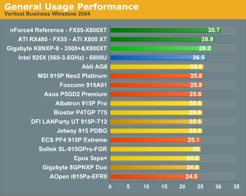
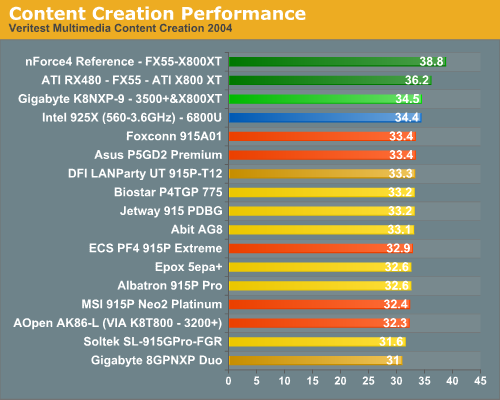
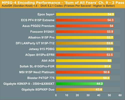
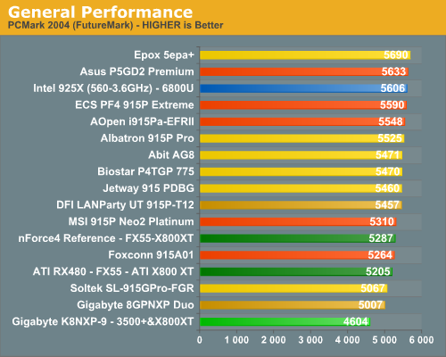
All tested motherboards were based on the same Intel 915 chipset and tested with the same CPU. The only difference was the memory supported by the board - either DDR or DDR2. So was DDR or DDR2 the winner? As we saw in our launch review for the 925X/915, the performance of fast DDR400 and DDR2-533 at aggressive timings is about the same. Having said that, some will still be surprised to see that there is really no winner in DDR or DDR2 in Winstones, even though we are comparing fast 2-2-2-5 DDR400 to fast DDR2-533 at 3-3-3-10. There is also no clear pattern of DDR2 or DDR performing better in these results. It appears that the performance is more dependent on the quality of the design than the type of memory used by the 915 board.
The same is true in results for PCMark 2004. There is a greater overall variation in PCmark scores, but no real pattern in terms of the type of memory used on the board. However, it is surprising to see such a wide range of results on PCMark 2004 tests on boards using the same chipset. The range of scores from 5000 to almost 5700 using the same CPU is extremely large. You will definitely see the performance difference in these boards. All the boards, but 4, are clustered between 5457 to 5690, but the bottom 4 boards are significantly slower with scores from 5007 to 5310.
2-pass Media Encoding results with AutoGk 1.6 and the DivX 5.2.1 Codec also reveal no clear performance pattern with either DDR or DDR2. You can choose either memory on a 915 board and be confident that performance will be competitive with other 915 boards and memory configurations.
One pattern that will emerge as we take a closer look at the benchmarks is that the same few motherboards are at the top of our test results over and over again. This will be even clearer in the DirectX 9 gaming tests. For those of you interested in comparisons to the Athlon 64, it is interesting that the FX55 totally dominates Winstones. On the other side, PCMark 2004 is dominated by the Intel boards. Clearly, both results cannot be correct, but are more a reflection of the design of each test and the features supported in each benchmark.
DirectX 9 Gaming Performance
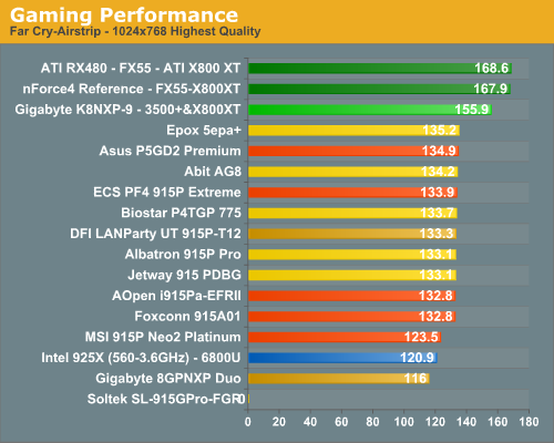
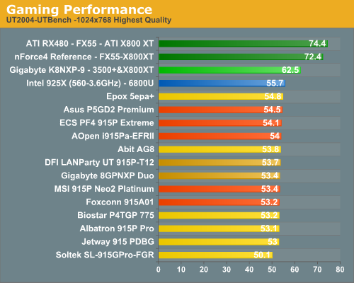
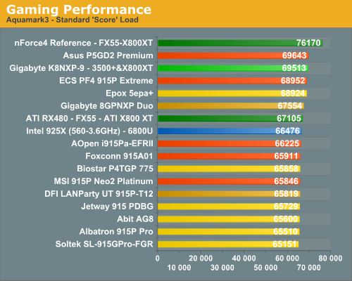
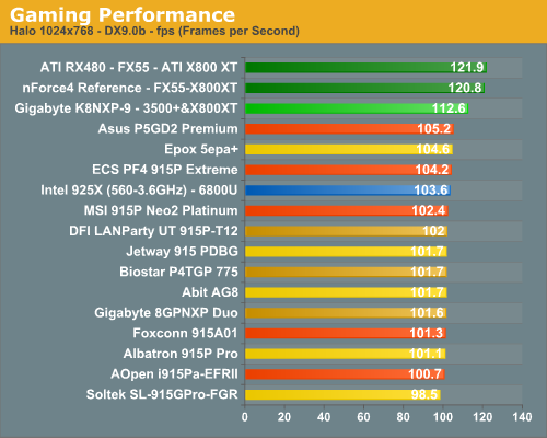
After the clustering of scores in Winstones, you may not have expected much variation in game benchmarks. That is why expectations get us all in trouble because there is a really a large variation in DX9 benchmarks. One thing is quite consistent across the DX9 tests, and that is the domination of performance results by the Asus P5GD2 and the Epox 5epa+. In every benchmark, either the Asus or Epox wins the test, and the other board is normally #2 or #3 in the worst case. Another board that is consistently at the top of the DirectX 9 benchmarks is the ECS PF4 915P Extreme, which will come as a surprise to many. It was certainly a surprise to this reviewer.
The other boards seem to shift positions in the middle, but we, again, have some consistency at the bottom of the performance results. The Soltek is consistently at the bottom of the performance charts, which certainly should not be a surprise, considering that it is the only board running our Fast DDR400 at DDR333 speed. We would expect that as soon as Soltek can fix this issue, the position of the Soltek will change relative to other boards in the 915 roundup.
One thing to keep in mind as you look at the benchmarks is the relative position of the top overclockers in this roundup. The Asus, Abit, Epox, MSI, Albatron, and DFI were our top overclockers in our tests, but clearly, they get to their high overclocks by different means. The MSI can reach 285 at the top, but is often near the bottom in stock performance. The DFI is pretty average at stock speeds, but it becomes a dynamo when challenged to an overclock. The Asus is a great overclocker, but it is also very fast at stock speeds. In other words, the Asus starts fast and stays fast through overclocking, making it a great choice for both stock performance and extreme overclocking.
DirectX 8 & Open GL Gaming Performance
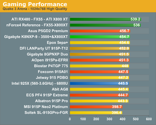
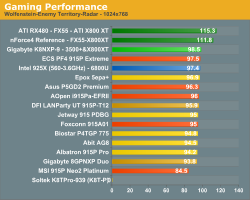
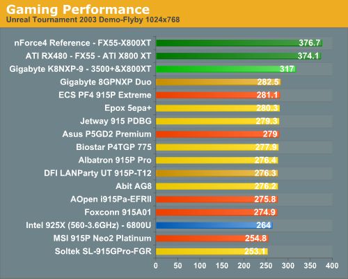
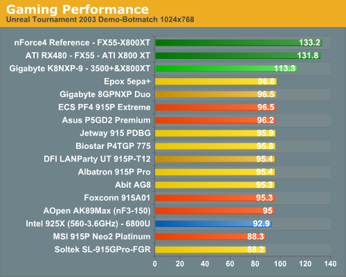
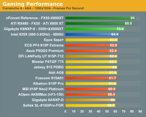
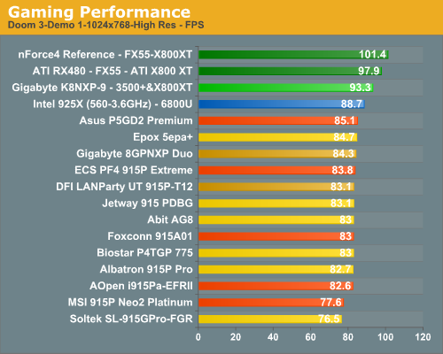
The same pattern of Asus, Epox and ECS at the top of the charts continues in DX8 and Open GL gaming. These 3 boards continue to land at or near the top in all the older game benchmarks. After many months of seeing the tight clustering of Athlon 64 scores, it is interesting to see the true impact of off-chip memory controllers on performance. This is not necessarily a good thing, since the on-CPU memory controller has made A64 performance very consistent across the same CPU on virtually any A64 chipset. Here, with the memory controller in the chipset, we are seeing much more variation in performance depending on the quality of the board design itself. This is true, even though all boards are using the same Intel 915 chipset.
As in the 925X, we were again surprised to see the very average performance of the DFI UT 915P-T12 at stock speeds. We are beginning to see the DFI as achieving some of its incredible overclocking powers because it is starting at a rather unimpressive performance level at stock speeds. Before you jump to conclusions here, compare the DFI results to the Asus P5GD2. The Asus is extremely fast at stock speeds - in fact, the fastest board in the roundup - but it is also an incredible overclocker. The Asus both starts fast and ends fast.
Final Words
As the testing for the 915 roundup dragged on day after day, we realized we had been spoiled in our tests of the Athlon 64 in the last 6 months. Why do we say that? We had become accustomed to very tight clustering of test results, mostly because the memory controller is on-chip in A64, and we were no longer accustomed to the wide range of performance results that we actually found in the 915 roundup. This is both good and bad. Consistency of results is a good thing when you can buy a Socket 939 motherboard and get similar results at stock speed no matter which board you buy. This is one of the reasons ATI, who had not been particularly strong in their memory controller designs for Intel boards, was able to hit a home run with their first Athlon 64 chipset design. It might not be such a good thing when you are Asus, who can clearly design a motherboard that will outperform the competition. There, the consistent results from an on-chip memory controller could kill the significant advantage that you would enjoy otherwise.This little exercise in self-indulgence is a prelude to the flak that we are sure will fly when we announce the winners and losers in this roundup. We expect flak because there really are a few clear winners here and there are also some dogs in the 915 camp. The difference between the top and bottom is also much larger than we would have ever expected when we began this project.
We have avoided the 915 chipset like the plague for the last 6 months - and so have our readers - voting their choices with their buying dollars. But all of this is about to change in the near future. Whether you like it or not, or approve or not, Intel is deciding for you that your next purchase of an Intel chipset board will be a 915 or 925X. You will either buy one of these, since the 865/875 stock is dwindling in supply, or you will have to opt for an Athlon 64 on a Socket 939 or 754. Frankly, many readers will move to Athlon 64, but others will want to stay in the Intel camp. That is not necessarily a bad thing, since performance and value can be found in the 915 boards that we reviewed. These boards will not compete with the Athlon 64 at the fastest A64 speeds, but in the mid-range - where most people actually buy - they are competent competitors and generally a good value for your money.
However, not all of the 915 boards are created equal, which is why you are reading this review. The purpose of any roundup is to help you find and buy the good stuff and avoid the poor performers. So, we do in fact have some recommendations.
The top performer and clearly undisputed winner in our 915 roundup is the Asus P5GD2. The Asus performs very fast at stock speeds, at the top of the heap, and it also reaches the highest overclocks that we have ever seen on our 560 ES (Prescott 3.6GHz) processor.
 |
Based on the best performance that we have ever achieved with a Prescott chip, stellar performance at stock speeds, the top-notch implementation of Intel 915/ICH6R features, the excellent enhancements to those features such as Stack Cool, Dolby Digital Live encoding, WiFi G networking, PCI Express LAN, high-speed 1394b firewire, and the best overclocking abilities of any 915 motherboard, we are pleased to award the AnandTech Gold Editors Choice to the Asus P5GD2 Premium. |
The P5GD2 is an expensive motherboard, at about $240 on the web, but you can get almost all the same features in the P5GD2 Deluxe for about $50 less. Either way, you will find value in the Asus P5GD2. It is a superb piece of motherboard engineering that pays off in top performance in every area.
The Silver Editors Choice is a tie between the DFI LANParty UT 915P-T12 and the Epox 5epa+. The 2 boards bring different capabilities to the table, but both are worthy of the Anandtech Silver Editor's Choice.
 |
We are pleased to recognize the DFI LANParty UT 915P-T12 as our Silver Editor's Choice in the 915 roundup. The DFI is one of the best overclocking 915 boards that we have tested with features to allow the Enthusiast to extract the highest overclocks possible from their 915/ Prescott CPU system. DFI was diligent in preserving 915 features and even enhancing them with choices like Karajan High-Definition audio and PCI Express Gigabit LAN - features that clearly make a difference in the performance of the 915 system. The DFI LANParty UT will bring a big smile to any Enthusiast's face. It is an easy board to learn to love. |
|
The Epox 5epa+ proved to be a top performer at stock speeds as well as an outstanding overclocker among motherboards based on the 915 chipset. As a result of the fast stock performance combined with the potential to extract the best performance when overclocking a 915 system, we recognize the Epox 5epa+ as Silver Editor's Choice in our 915 roundup. Audio and Gigabit LAN are thin in this Epox design, but overall performance and value for your dollar are very satisfying. Epox is to be congratulated on their excellent 915 chipset motherboard. |
 |
The ECS PF4 915P Extreme was a consistent top performer compared to other 915 boards. It also features a reasonable selection of overclocking options and a really excellent choice of features for a 915 motherboard. These include Azalia High Definition audio, Dual LAN, and the addition of IDE ports with the SiS 180 controller than will be appreciated by many users. In recognition of the great value and performance represented by the PF4 915P Extreme, we are pleased to recognize ECS with our Bronze Editor's Choice award. |
While we tested 13 boards plus reference boards from nVidia, ATI, and Intel, this 915 roundup represents performance results for about 23 motherboards in the AnandTech labs. With such a large roundup, we wish we could recognize more motherboards deserving of praise for excellence in a number of performance areas. However, we think that you will agree that the four motherboards, which rose to the top of the 915 roundup, represent some of the best performance and value available among 915 boards.
Some will argue that none of the 915 boards deserve recognition, since the group is clearly outperformed in our benchmarks by Athlon 64 Reference Boards. We disagree, since the 4 top boards here represent value and performance for your buying dollar. If you want the top performance, by all means go for a top Athlon 64 board. If you insist on Intel, or you are looking for good value for your dollar, then one of these four top 915 boards will serve you very well.


