Original Link: https://www.anandtech.com/show/15493/hygon-dhyana-reviewed-chinese-x86-cpus-amd
Testing a Chinese x86 CPU: A Deep Dive into Zen-based Hygon Dhyana Processors
by Dr. Ian Cutress & Wendell Wilson on February 27, 2020 9:00 AM EST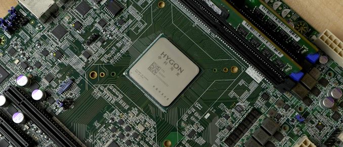
In 2016, through a series of joint ventures and created companies, AMD licensed the design of its first generation Zen x86 processors to be sold into China. The goal of this was two-fold: China wanted a ‘home grown’ solution for high-performance x86 compute, and AMD at the time needed a cash injection. The outcome of this web of businesses was the Hygon Dhyana range of processors, which ranged from commercial to server use. Due to the Zen 1 design on which it was based, it has been assumed that the performance was in line with Ryzen 1000 and Naples EPYC, and no-one in the west has publicly tested the hardware. Thanks to a collaboration with our friend Wendell Wilson over at YouTube channel Level1Techs, we now have the first full review of the Hygon CPUs.
Let’s Start From The Beginning
There are two/three primary manufacturers of x86 processors: Intel, AMD, and Via/Centaur. Both Intel and AMD have been competing in the high performance compute space for multiple decades, and the reason there hasn’t been any other competitors is due to licensing. Due to patents surrounding the x86 architecture, Intel doesn’t want anyone else coming in and treading on its market share dominance, and to complicate matters, it is AMD’s version of 64-bit x86 that is currently being used by all involved. Intel and AMD are inextricably linked in this way. Meanwhile. Via/Centaur is along for the ride, with a very small market share mostly in Asia, and a lack of a leading edge high performance competitor.
For those who haven’t been following AMD, the company has been through a number of ups and downs. A significant down was during its Bulldozer CPU architecture years, where costs were high, performance wasn’t great, and Intel pulled ahead significantly in all areas: laptop, desktop, commercial, and enterprise. The design of Intel’s CPUs and its market dominance strategy, combined with the lack of a leading edge competitive product for AMD along with the purchase of graphics IP company ATI, nearly bankrupted AMD. Through the leadership of the former CEO, Rory Read, AMD became stable, and under the auspices of current CEO Dr. Lisa Su, the company put heavy investment back into its x86 CPU design. At one point, AMD’s debt was higher than its tangible assets, and the company had to even sell its headquarters and lease the buildings back from the new owners to find the funds to stay afloat.
Another element of this ‘staying alive’ tactic was the sublicensing of AMD’s x86 IP, which ultimately created the Hygon Dhyana x86 processors for China. Some people will quote this as being a keystone for AMD staying alive, however it is of a general consensus that this sublicensing ultimately secured AMD only around $200m (until the US entity list ban) out of the original $293m deal. At that time AMD was already making quick strides into the consumer market with its Ryzen 1000-series processors, which offered eight cores with modestly competitive performance while beating Intel on performance-per-dollar, giving AMD enough to reinvest in its key areas. The sublicensing ultimately provided AMD more of a safety net, depending on the success of the first generation Ryzen product portfolio.
AMD Does Due Diligence
Simply stating ‘AMD sublicensed the IP of one of its x86 designs’ sounds a bit farfetched on most days of the week. If either AMD or Intel believed that the opportunity to let others sell its CPU designs was profitable, how come it took until 2015/2016 to ever come to fruition? Part of this story covers that while there was clearly some money in it for AMD here, it didn’t fall foul of any Intel-AMD licensing agreements. And most importantly, it didn’t contravene any US laws regarding the export of high-performance computing intellectual property.
This last point is important. The US government gives every CPU that comes out of Intel, AMD, and others, a value based on its performance. This is some combination of FLOPs and power, and those that surpass a specific threshold are deemed too powerful to be sold in certain markets. This includes semi-custom processors, where AMD/Intel fiddle with the core count/frequency and provide off-roadmap parts.
AMD at the time made the following statement:
Starting in 2015, AMD diligently and proactively briefed the Department of Defense, the Department of Commerce and multiple other agencies within the U.S. Government before entering into the joint ventures. AMD received no objections whatsoever from any agency to the formation of the joint ventures or to the transfer of technology – technology which was of lower performance than other commercially available processors. In fact, prior to the formation of the joint ventures and the transfer of technology, the Department of Commerce notified AMD that the technology proposed was not restricted or otherwise prohibited from being transferred. Given this clear feedback, AMD moved ahead with the joint ventures.
AMD had contacted the DoD and DoC, as well as all others, and had been given the green light. The new microarchitecture was deemed of low enough performance to not hit any of the export bans. AMD was also given crystal clear confirmation that the ‘technology proposed was not restricted or otherwise prohibited from being transferred’, which is a rather stark statement. At this point it should be clear that AMD may have submitted a modified version of its IP to the relevant US departments, rather than the microarchitecture we saw in the Ryzen 1000-series. This is part of what this review is about.
Joint Venture in a Joint Venture
The end goal of all of this was to be able to provide China a version of AMD’s Zen 1 CPUs that could be called ‘Chinese’, rather than ‘American’. As has been the case of the last decade or more, China has wanted to rely less on American technology and intellectual property in order to become self-sufficient. The way in which AMD’s joint ventures worked for the Hygon Dhyana designs was built to essentially do that in a very roundabout way.
The name of the joint venture overseeing the operation is called THATIC, or Tianjin Haiguang Advanced Technology Investment Co. Ltd. This company is owned by AMD and a mix of Chinese companies, both public and private, including the Chinese Academy of Sciences, but is at least 51% owned by AMD.
Two companies were created in order to perform the web of steps required – these companies would be jointly owned between AMD and THATIC (note that AMD also owns part of THATIC). These companies are:
- HMC: Haiguang Microelectronics Co. Ltd.
- Hygon: Chengdu Haiguang Integrated Circuit Design Co. Ltd.
Of these companies,
- HMC is 51% owned by AMD and 49% by THATIC.
- Hygon is 30% owned by AMD, and 70% by THATIC.
These companies fulfill different roles in the chain. HMC works with AMD for design and GlobalFoundries for manufacturing, while Hygon works with HMC to add co-design elements and packaging, then selling the silicon to China.
Licensing Core IP is Different to Sub-Licensing x86
A lot of confusion was made when the creation of the THATIC joint venture happened. The big overriding question was if AMD had somehow licensed the full x86 (and x64) architectures to a Chinese company, allowing them to build fully capable custom x86 CPUs and push both Intel and AMD out of the market there. This is not the case with the joint venture.
What AMD did was license a single core design to HMC, along with an SoC layout. From this point on, AMD is officially ‘hands-off’, but AMD engineers and executives are involved at HMC, so technically they are still present. With these core designs and SoC layouts, HMC sent the floorplans, not the RTL, to Hygon for requested updates. Hygon submitted the updates to HMC, which were either approved or rejected by AMD’s engineers. HMC would integrate the changes, and then take orders from Hygon for manufacturing. With Hygon’s order, HMC went to GlobalFoundries with the design and ordered the silicon. HMC then sold the silicon to Hygon, which packages the CPU into various configurations and sells it into the Chinese market. It is also up to Hygon to help design motherboards for the new platform(s).
Broken down into steps:
- AMD licenses core design to HMC with suggested SoC layouts
- HMC provides floorplan to Hygon
- Hygon suggests changes to HMC
- AMD engineers at HMC approve/reject changes
- HMC offers final floorplan to Hygon, ready to take orders
- Hygon orders wafers / silicon die from HMC
- HMC approaches GlobalFoundries for manufacturing
- GlobalFoundries achieves particular frequency/yield on new design
- HMC sells completed silicon to Hygon
- Hygon performs packaging on the silicon in China
- Hygon sells completed CPUs into China
Because HMC is the one providing Hygon with the IP, the CPU can now be classified as ‘Chinese’, despite the underlying design coming from AMD.
When AMD announced the creation of THATIC, it spoke about sub-licensing its Zen core IP to the joint venture. It was described as a multi-year partnership, however it was confirmed at a trade show that AMD was only sub-licensing a single version of its IP, and that there were no plans to sub-license any others in the works.
At the time, it was assumed that AMD had sub-licensed the same version of its Zen core IP that had already been released as the Ryzen 1000-series processors and EPYC Naples processors. However as part of this review will show, it would appear that AMD made some performance changes to the design before it was given to the joint venture – specific instructions have a lower throughput than what we saw from the processors coming directly out of AMD.
Not only this, but in that list of steps, point (4) is most apt. Hygon requested specific changes for the Chinese market. Before everyone leaps to ‘creating backdoors for the Chinese government’, we know of several modifications that were made due to Linux kernel updates. In China different elliptic cryptographic algorithms are used compared to the west, and so the hardware accelerated functions for these were changed, and different microcode used in order to enable these. Part of this review is to try and discover if there are any other changes as well.
The final product out of this spider web of arrangements is the Hygon Dhyana x86 core, an ‘updated Zen core for China’, which Hygon packaged for both embedded, commercial, and enterprise systems. We saw at Computex 2018 that Chinese server vendor Sugon was involved in this project, with the company showcasing its servers built on 32-core Hygon CPUs. Users that follow online benchmark databases also saw submissions for 8-core commercial and embedded variants, likely to be used for government and education deployments.
We should point out that we asked AMD several times what differences were in the Hygon Dhyana designs compared to the original Zen 1 cores. With ‘AMD’ playing a limited role in all of this, we were simply told that if we could get hold of one, if we identified changes to the design in our testing, they might consider confirming or denying them. For as open as AMD has been with us about the Ryzen and EPYC processor families, it was a stark contrast when talking about Hygon.
The first Hygon CPUs went into the Chinese market in 2018, however they were almost impossible to source. The Hygon CPUs were never meant to be sold to the west, and the nature of the CPU and the companies dealing with it meant that none that we could identify were ever interested in sampling us.
In 2019, the US created an ‘entity list’ of Chinese companies what are deemed a potential security threat to the US market. As a result, any commercial interaction with these companies, with products or IP that were at least 25% created in the US, are restricted and forbidden. THATIC was one of the companies placed on the list, which means that AMD can no longer license any additional IP to the joint venture. THATIC still has access to the original IP it licensed however, and can continue to manage it (albeit without AMD’s assistance), however the ban also restricts HMC’s ability to order silicon from GlobalFoundries, making the whole process in limbo if not defunct.
A big thanks to Usman Pirzada’s great write up, from which much of this was based on, as well as Drew Prairie from AMD who has provided additional context to AMD’s arrangement.
Working with Wendell: Sourcing Hygon CPUs
For this review, we were able to test two systems remotely housed in the lab of Wendell Wilson, the charismatic host of the Level1Techs YouTube channel. We were both approached by sources asking if we wanted to purchase systems, which we gather were old engineering samples from a Hygon or Sugon subsidiary based in the US that was performing post-manufacturing analysis and performance testing. That subsidiary has now been dissolved, a knock-on effect of the entity list ban, and the engineering hardware within that company was (unbeknown to us) sold off. We were given the opportunity to borrow a couple of systems that fell out of the dissolution. Due to location, Wendell offered to house them, take some pictures and video, while we both did performance benchmarks. Linus’ team from the popular LinusTechTips channel were also invited to participate – you can see the video that was produced here.
Ultimately we ended up with two systems to test – one commercial ‘Hygon Dhyana’ and one enterprise ‘Hygon Dhyana Plus’.
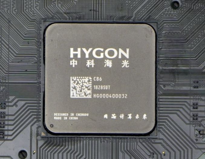
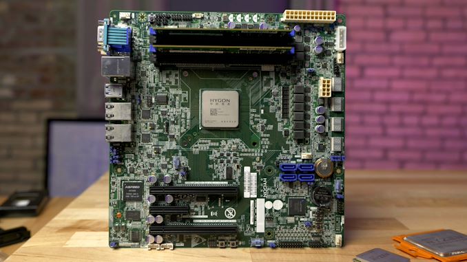
The commercial system looks like a normal 8-core Ryzen 1000-series system, however it is actually a BGA design and is not upgradeable. In fact this seems to be an early engineering sample, as the CPU doesn’t even have a number associated with it. There’s also something interesting going on with the mounting points, which we’ll cover in due course.
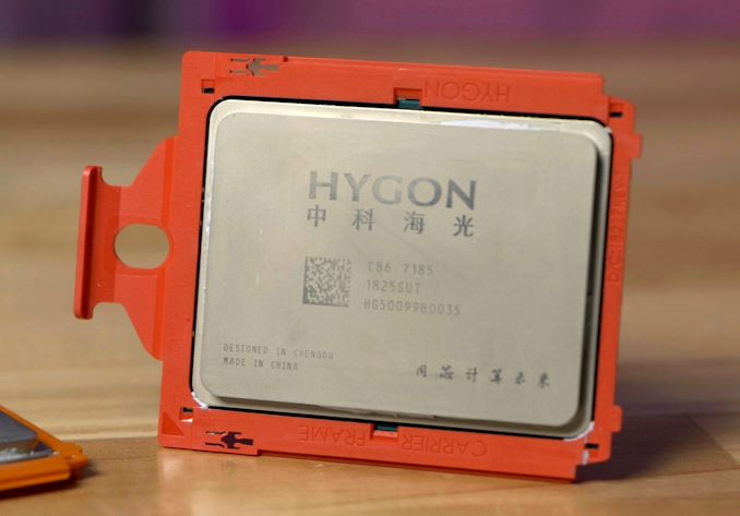
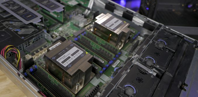
The enterprise system is a dual 32-core Hygon 2U server. These CPUs state that they are the ‘7185’ models, which we know to be the highest core count that Hygon offered, and one of the highest performance 32-core parts as well. Putting two of them into a server looks very much like a 2P EPYC Naples design.
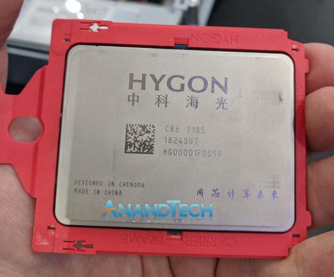
It should be noted that we did see a Hygon processor before at a trade show, and you may notice some Chinese writing at the bottom. Interestingly enough, we got the bottom right of the CPU translated. A literal translation is
'Using Cores to Calculate The Future'
However, the second character used in the slogan is a homonym, which could be translated as:
'Using Passion to Calculate The Future'
Over the next couple of pages we’ll examine the two systems in more detail, and then a look into the fundamental differences we found at a core and SoC level compared to the Ryzen 1000 and EPYC Naples processors we’ve already tested in years gone by.
Our Hygon Systems
8-core Dhyana and Dual 32-core Dhyana Plus
The full range of Hygon’s known releases boils down to two platforms: one containing a single 8-core Zen 1 die, similar to the desktop range of processors (or EPYC 3000), and a set of server processors built from four dies in a similar arrangement to Naples.
The 8-core engineering sample system we have in to test didn’t provide any exact SKU numbering – on the CPU it says ‘C86’ which is meant to imply ‘Chinese x86’. The rest of the numbering is likely linked to the wafer and batch that this silicon came from, however we do not have decoder rings for those.
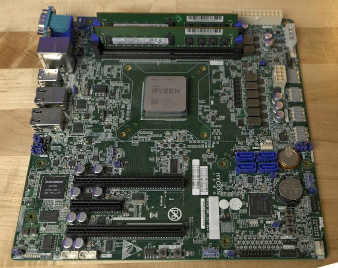
The motherboard uses a microATX form factor, and is very much a server motherboard with the DDR4 slots horizontal rather than vertical in order to direct airflow through the system in a server chassis. Starting primarily with the socket, what we have is a non-socketed BGA design, such that this CPU cannot be upgraded because it is bonded to the motherboard, similar to what we see with laptops and embedded systems. The mounting holes are the thing that surprises me here – these are not the AM4 mounting holes that we typically see with the consumer version of Ryzen, but these mounting holes are Intel mounting holes. Someone must have a lot of old Intel coolers around, I guess? Either that or it makes it easier for Hygon’s partners to find specific server grade coolers.
The CPU has a six-phase power delivery system, and as this is a pure CPU product, there is no integrated graphics. There is a form of 2D graphics provided by the IPMI controller in the bottom left, the classic ASPEED AST2500 chip that we commonly see in server systems. Unlike other microATX motherboards, there isn’t the typical four slot design here, but a three slot design, with two full length PCIe 3.0 slots (capable of x16/x0 or x8/x8) and an open ended PCIe x4 slot.
Normally these CPUs don’t really need a chipset because they have some SoC level IO functionality on the silicon, though consumer Ryzen CPUs were paired with X370 chipsets when the Ryzen 1000 family first launched. Instead of using those chipsets, Hygon has paired the CPU with a Lattice Semiconductor FPGA to act as a chipset of sorts. This gives the motherboard an odd set of combined IO, including SATA ports, four dual LED displays, a number of custom connectors and buttons, and a lot of undocumented things we don’t know. For example, there appears to be two batteries on the motherboard – one presumably to keep the onboard time, but the other seems more permanent and is not obvious why it is there.
Here’s the motherboard where we’ve put an equivalent AM4 consumer Ryzen CPU on top, to show the size.
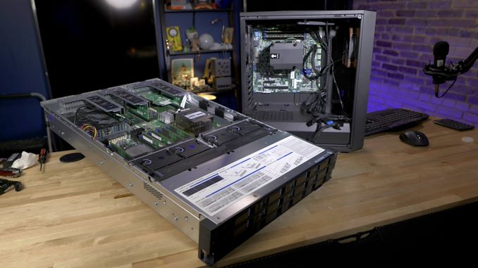
By comparison, the dual socket server is a bit of a beast. As we understand it, these servers were built for both compute and storage, with each CPU paired with four breakout connectors capable of four U.2 drives or 16-way SATA connectivity. The CPUs have eight channel memory capabilities, but due to a couple of reasons we had to test them in quad channel mode.
The CPUs in this case also say C86, but also have the model number 7185 on them, indicating a 32-core CPU. The carry case is red, whereas Naples EPYC CPUs were blue, Threadripper CPUs are orange, and Rome EPYC CPUs are green. The red might be a nod to the Chinese angle for these CPUs, however no-one we spoke to was able to confirm this.
The server is actually a Sugon design, with 12 front panel 2.5-inch drive slots. For the 8-core system, that was put into a standard desktop case and fitted with a CPU cooler. Both systems were tested though remote desktop access, as Wendell was hosting them in his labs in Kentucky while I’m all the way back in London.
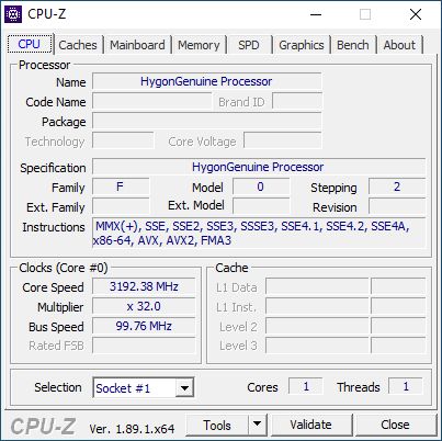
When trying to probe the CPUs, CPU-Z didn’t seem to have much of a clue. The software provided this interface on the 8-core consumer, showing a 3.2 GHz frequency, but only one core, and no other details aside from support for AVX, AVX2, and FMA3. For the server CPUs, CPU-Z failed to run at all. What we were able to determine is that the software thought that every core was a separate socket, and it appears that some of the usual ways to access this data on the AMD consumer CPUs have all been changed here for the Hygon models, either to evade detection using usual methods, or to conform to different standards. One interesting note is that while CPU-Z detected AVX and AVX2, some of our software couldn’t, and we had to revert to SSE detection in order to get that software to even run.
Hygon CPUs: Chinese Crypto, Different Performance
The big overriding question is about what exactly has changed with these processors compared to the standard Ryzen and EPYC CPUs. To say that they are rebadged processors, as some have suspected, is completely incorrect – we can tell this alone by the different cryptography engines provided by the Linux kernel updates. But we also detected other differences.
By and large, as we could determine, the core layout is identical, with the same cache sizes, TLB sizes, and port allocations – there were no differences at this fundamental level. The CPU still offered 64 KB 4-way for the L1 instruction cache, 32 KB 8-way for the L1 data cache, 512 KB 8-way for the L2 cache, and 8 MB 16-way for the L3 cache, identical to the Zen 1 core. TLB entries are as follows:
- L1D + L1I: 4K/2M/1G 64-entry
- L2D: 4K 1536-entry 6-way, 2M 1536-entry 3-way, no 1G
- L2I: 4K/2M 1024-entry 8-way, no 1G
Memory access times are 4 cycles for L1, 12 cycles for L2, and 37-40 cycles for L3. Memory latency was measured at 284-307 cycles.
L1 read speeds were measured around 32 bytes per clock (805 GB/s total, ~100 GB/s per core), while write speeds were measured around 16 bytes per clock (408 GB/s total, ~51 GB/s per core). DDR4 Memory speed for the 8-core gave 38.5 GB/s for reads and 35.8 GB/s for writes.
Cryptography Changes
For the cryptography changes, these are detailed in the Linux kernel updates. The updates revolve around AMD’s secure encryption for virtualization features, or SEV. Normally with an EPYC processor, SEV is governed by the cryptography protocols defined by AMD, in this case RSA, ECDSA, ECDH, SHA, and AES. In order to generate the right keys, SEV uses these methods. However, in the Hygon Dhyana designs, SEV is built to use algorithms known as SM2, SM3, and SM4.
As stated in the updates, SM2 is based on elliptic curve cryptography, and requires additional private/public key exchange. SM3 is a hashing algorithm, similar to SHA-256, and SM4 is a block cipher algorithm, similar to AES-128. Additional commands are placed into the Linux kernel in order to support the extra functions these algorithms need. In the notes it states that these algorithms were successfully tested on Hygon Dhyana Plus (presumably the big CPU) processors but they were also successfully tested on AMD’s EPYC CPUs.
Slowing Down Some Instructions
The biggest update to the design we were able to determine is in the instruction throughput. We don’t think that this difference between Dhyana Plus and EPYC has been mentioned before, and we did extra checks to make sure our software was displaying the right data, but put simply some instructions have been purposefully made slower. This has some rather serious implications, especially depending on when it occurred in the pipeline.
What we think is the case is that in order for AMD to export its SoC design, it had to also share microcode relating to how the CPU interprets instructions, and it was told to slow down certain key instructions (or disable them altogether) in order to make the arrangement with the joint venture and China work.
In our testing, we found that while integer performance is similar between Hygon and EPYC, certain floating point instructions, namely DIV and SQRT, are not pipelined in the Hygon CPU. This means throughput and latency is reduced. A lot of simple MMX/SSE instructions have reduced throughput:
| Instruction Throughput Differences | ||
| AnandTech | EPYC Naples |
Hygon Dhyana |
| ADD/SUB | 2 per clock | 1 per clock |
| CMP/MULP* | 2 per clock | 1 per clock |
| ADDSUBP* | 2 per clock | 1 per clock |
| RCP*/RSQRT* | 1 per clock | 0.5 per clock |
| BLENDW | 3 per clock | 2 per clock |
| PMIN/MAX* | 3 per clock | 2 per clcok |
| PAND/ANDN/OR/XOR | 4 per clock | 2 per clock |
| MOVs | 4 per clock | 2 per clock |
All of these instructions are pretty important for even basic tasks. By limiting the simultaneous throughput of these instructions, it means that these CPUs cannot compute code that can be parallelized as fast, ultimately decreasing performance.
Perhaps the biggest change however was one that even differed between the server ‘Dhyana Plus’ processor and the consumer ‘Dhyana’ version. Random number generation, which is a key backbone in a lot of stochastic and financial processes, is severely reduced on the Dhyana Plus. The key instructions, RDRAND and RDSEED, have various reasons for being slow/fast. Here’s the comparison:
| Instruction Latency Differences | |||
| AnandTech | Zen 1 Desktop |
Hygon Dhyana |
Hygon Dhyana Plus |
| RDRAND | |||
| 16-bit | 1200 clocks | 1100 clocks | 800 clocks |
| 32-bit | 1200 clocks | 1100 clocks | 800 clocks |
| 64-bit | 2365 clocks | 2125 clocks | 1520 clocks |
| RDSEED | |||
| 16-bit | 1200 clocks | 1100 clocks | 12000 clocks |
| 32-bit | 1200 clocks | 1100 clocks | 12000 clocks |
| 64-bit | 2365 clocks | 2125 clocks | 27100 clocks |
That’s quite a difference, especially in RDSEED. We saw that RDSEED, the seed generation to help spawn random number algorithms, is over 10x slower on the server chip, and RDRAND, used for actually generating hardware based random numbers, is faster than standard Ryzen – moreso on the server chip. Interestingly enough, the same delays for RDSEED for the server chips are also seen on Ryzen Mobile and Ryzen Desktop APUs.
For RDRAND, having a faster random number generator can be indicative of two things: either it is actually faster, or the random algorithm has a lower periodicity, i.e. the point at which an algorithm wraps on itself. The best pseudo-RNG have the largest periodicity, so in this case the RDRAND is fast leads us to conclude that the periodicity is low, leading to lower quality random numbers.
For RDSEED, the fact that this is 10x slower is a little different. RDSEED is meant to take information from the various sensors on board and output a random value to initialize the RDRAND – it should only get called once per periodicity. A slower RDSEED either means its taking data from more sources (a good thing), or it’s being slowed down on purpose (a bad thing).
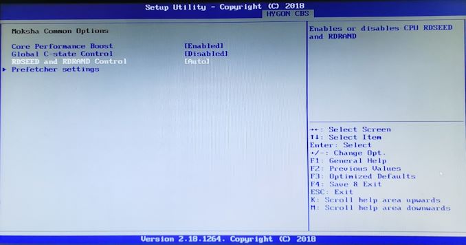
In actual fact, RDRAND and RDSEED can be enabled/disabled in the BIOS of our Dhyana Plus system.
It’s amusing that this menu is called ‘Moksha Common Options’. Moksha being a word commonly associated with ‘enlightenment’ or ‘release’. This is either a clever word play, or someone digging out a non-contextual old Chinese to English dictionary in translation.
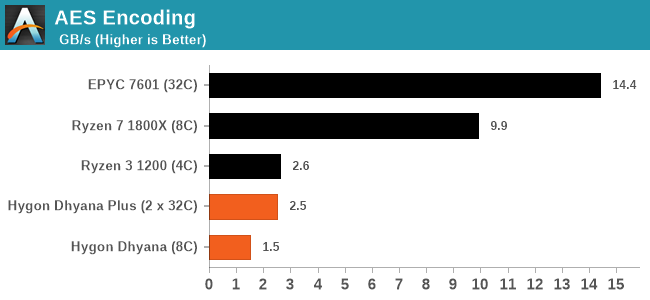
When it comes to AVX and AVX2 performance, even though the CPUs were able to identify themselves as having AVX and AVX2 support, trying to actually measure these instructions failed – in our instruction dumps, they were listed as ‘supported, disabled’. When it comes to supported features, Zen 1 typically lists AESNI, SHA, CLMUL, FMA4, BMI and BMI2 as supported instructions - none of these instructions are supported on the Hygon CPUs.
For things like AES, we have a direct benchmark for these, and the fact that these CPUs do not support AES means that we get a tanking in performance:
It should also be noted that the typical methods for finding the power consumption on AMD CPUs by probing registers also failed here. These seem to be removed from the CPU altogether.
Benchmarks: Windows
For both systems, we installed Windows: Windows 10 Pro on the small 8-core Dhyana system, and Windows 10 Enterprise on the big dual 32-core Dhyana Plus server. With AVX/AVX2 not working properly, our range of testing was limited. As mentioned previously, some software didn’t even want to run on one system or the other, such as CPU-Z on the server.
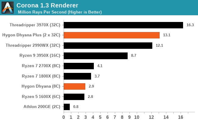
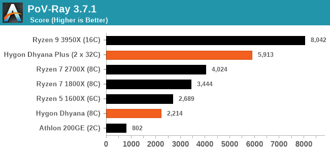
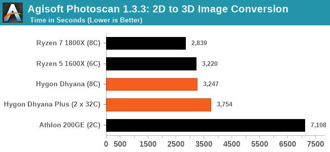
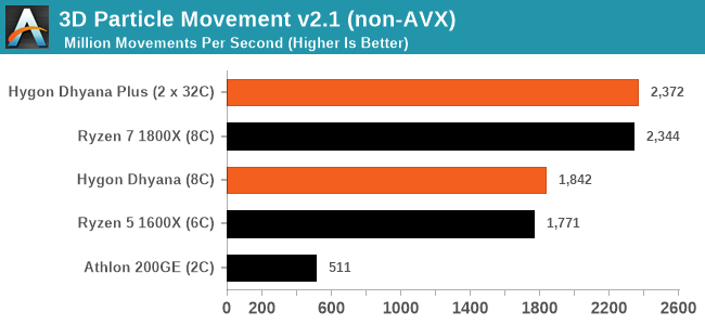
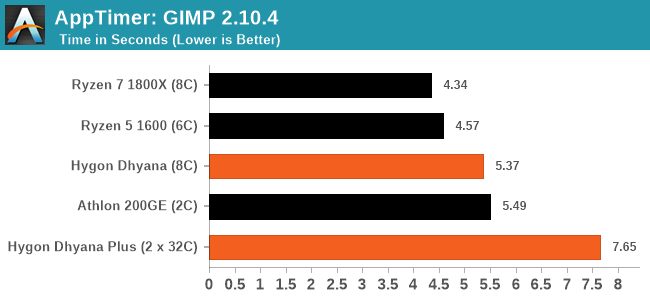


From the numbers we can see that our 8-core Dhyana processor falls somewhere between the 6-core Ryzen 5 1600X and the 8-core Ryzen 6 1800X, due to clock speeds, but on particular tests it gets hammered by even the Athlon 200GE. The dual 32-core Dhyana Plus server seems to be in all sorts of a mess, often beaten by the Ryzen 7 1800X, or can now be easily beaten by the Ryzen 9 3950X. The one benchmark where it did really well was Corona – a memory/NUMA agnostic integer based renderer – it seems like a match made in heaven.
Hygon be Bygon
Every processor made in the US has to be of a certain performance level in order to be deemed suitable for export. Companies have pages and pages of documents relating to the performance of their hardware as determined by the metrics that govern the laws in the USA. These metrics include raw processing power, measured in gigaflops (GFLOPs), adjusted peak performance (APP), and/or the composite theoretical performance (CTP). Depending on which territory you export to, one or more of these metrics may apply.
One way around this, if you cannot import the CPU, is to have a license to build it. But more than that, if you can adjust the license and have a custom input into the design, you can relabel the hardware as a homespun device and be somewhat within the realms of plausibility. This is how one of AMD’s core designs, with modifications, has made it into a ‘Chinese’ x86 CPU for the Chinese market. The big plus on the packaging isn’t so much that it avoids import issues, but the ‘中国’ label that comes attached. Then again, one assumes that the people using these CPUs don’t exactly have a choice in what they can buy.
We discovered that these processors have been changed from the Zen 1 design in a number of ways. To say they are carbon copies of the Zen 1 SoCs, which is what a lot of people have suspected, is not true – enough has changed in the design to say that these parts are rebalanced, mostly for worse performance than their Zen 1 counterparts. The integer performance is essentially identical, however the floating point performance has been reduced – common instructions having half the throughput, and random number generation has been adjusted to be both slow and produce lower quality random numbers. The cryptography engines have also been replaced, such that common AES instructions are no longer accelerated but others more specific to the Chinese security, such as SM2, SM3, and SM4, are now included. In our testing, despite the processors showing AVX/AVX2 support when probed, it appeared to be disabled. We suspect this to be more of a firmware bug than a limitation of the Hygon CPU.
The method by which AMD was able to get an edited version of its first generation Zen core design into a ‘Chinese’ designed x86 CPU is highly convoluted. By first creating a joint venture with other Chinese companies called THATIC, then by forming two companies called HMC and Hygon each owned in different amounts between AMD and THATIC, how each business was able to discuss and control parts of the IP was sculpted in order to keep the secret sauce still in AMD’s hands, but allow the Chinese side of the ventures to request modifications. Those requests have to then be approved, and then HMC commissions the chips from GlobalFoundries, while Hygon packages them and sells them to companies like Sugon. We go into detail on this in our overview back on the first page, but suffice to say trying to follow where all the pieces are is almost like playing a game of Risk blindfolded.
With AMD unwilling to discuss on the record any of the finer details of the arrangement or changes to the processors, when asked if they could disclose how the processors were changed, we were told ‘if you find anything out, we may confirm it’. The one time I was able to see a Hygon Dhyana processor was due to a miscommunication with one of the Hygon vendors at Computex, and the person who let me take pictures suddenly stopped communicating with me after the event (I presume to keep his job). It still took over a year from those discussions to get hold of the chips for testing, and only then we were able to obtain the chips due to the current US Entity List ban covering one of the joint venture companies. This essentially killed the project dead, and caused one of the US subsidiaries to be mothballed, allowing some parts to leak onto the market where they had once been meticulously controlled.
Overall these Hygon CPUs offered China an alternative to the Intel market, and arguably something faster than they might have been able to purchase through import restrictions. AMD made some money at a time it badly needed it, but with the success of its Zen 2 platform, I don’t foresee AMD needing to do something similar over the next decade. The nature of the agreement between AMD, its joint venture THATIC, and the joint companies, was only for a single core design, Zen 1, and not Zen 2, limiting its competitiveness. Moreover, the US Entity List ban on one of the joint venture companies, for all intents and purposes, has made the project dead. The Chinese Hygon Dhyana x86 processors will still be in use by governments and other such organizations for a number of years to come, but this is bound to end up one of the oddest annals of the history of semiconductors.

