Original Link: https://www.anandtech.com/show/14733/sk-hynix-announces-36-gbps-hbm2e-memory-for-2020
SK Hynix Announces 3.6 Gbps HBM2E Memory For 2020: 1.8 TB/sec For Next-Gen Accelerators
by Ryan Smith on August 12, 2019 10:00 AM EST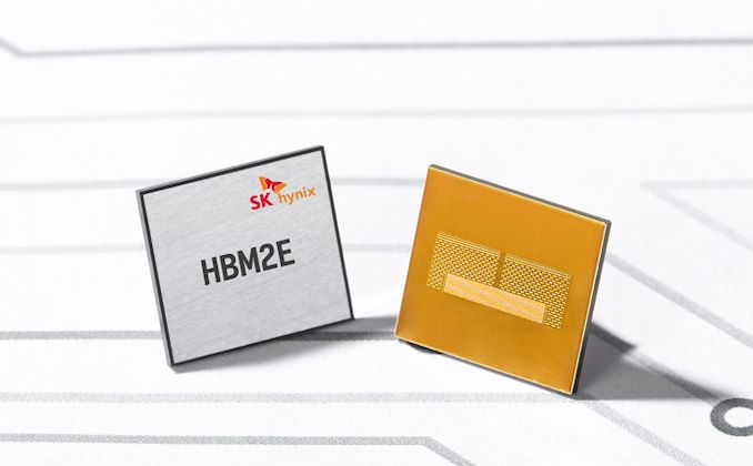
SK Hynix this morning has thrown their hat into the ring as the second company to announce memory based on the HBM2E standard. While the company isn’t using any kind of flash name for the memory (ala Samsung’s Flashbolt), the idea is the same: releasing faster and higher density HBM2 memory for the next generation of high-end processors. Hynix’s HBM2E memory will reach up to 3.6 Gbps, which as things currently stand, will make it the fastest HBM2E memory on the market when it ships in 2020.
As a quick refresher, HBM2E is a small update to the HBM2 standard to improve its performance, serving as a mid-generational kicker of sorts to allow for higher clockspeeds, higher densities (up to 24GB with 12 layers), and the underlying changes that are required to make those happen. Samsung was the first memory vendor to announce HBM2E memory earlier this year, with their 16GB/stack Flashbolt memory, which runs at up to 3.2 Gbps. At the time, Samsung did not announce a release date, and to the best of our knowledge, mass production still hasn’t begun.
Not to be left behind, SK Hynix is now also readying their own HBM2E memory. In terms of performance, SK Hynix says that their memory will be able to clock at up to 3.6 Gbps/pin, which would give a full 1024-pin stack a total of 460GB/sec of memory bandwidth, and in the process the lead for HBM2E memory speeds. And for more advanced devices which employ multiple stacks (e.g. server GPUs), this means a 4-stack processor could be paired up with as much as 1.84TB/sec of memory bandwidth, a massive amount by any measure. Meanwhile their capacity is doubling, from 8 Gb/layer to 16 Gb/layer, allowing a full 8-Hi stack to reach a total of 16GB. It’s worth noting that the revised HBM2 standard actually allows for 12-Hi stacks, for a total of 24GB/stack, however we’ve yet to see anyone announce memory quite that dense.
Given SK Hynix’s announcement, it’s interesting to note just how quickly HBM2 memory speeds have ramped up here: HBM2 vendors could barely do 1.9 Gbps 24 months ago, and now we’re looking at a near doubling of memory speeds in 3 years. This is a rather significant gain in a short period of time, especially with only a minor revision to the HBM2 spec being required. That said, I remain curious as to how SK Hynix (and Samsung) are going to deal with the heat of an 8-Hi stack running at those clocks; the HBM design philosophy is wide-and-slow, and 3.6 Gbps arguably isn’t so slow.
With their HBM2E memory set to go into mass production in 2020, SK Hynix expects the new memory to be used on “supercomputers, machine learning, and artificial intelligence systems that require the maximum level of memory performance.” All of these are distinctly high-end applications where HBM2 is already being heavily used today, so HBM2E is a natural extension to that market. At the same time, it’s also a reflection of the price/margins that HBM2 carries. HBM2 has remained (stubbornly) high-priced well after its release – a situation that memory manufacturers seem to be perfectly content with – and we’re not expecting HBM2E to change that. So expect to see SK Hynix’s HBM2E memory remain the domain of servers and other high-end equipment.
Source: SK Hynix


