Original Link: https://www.anandtech.com/show/14525/amd-zen-2-microarchitecture-analysis-ryzen-3000-and-epyc-rome
AMD Zen 2 Microarchitecture Analysis: Ryzen 3000 and EPYC Rome
by Dr. Ian Cutress on June 10, 2019 7:22 PM EST- Posted in
- CPUs
- AMD
- Ryzen
- EPYC
- Infinity Fabric
- PCIe 4.0
- Zen 2
- Rome
- Ryzen 3000
- Ryzen 3rd Gen
Editor's Note: With Zen 2 set to launch tomorrow (7/7), here's our architecture analysis from last month for some timely background information.
We have been teased with AMD’s next generation processor products for over a year. The new chiplet design has been heralded as a significant breakthrough in driving performance and scalability, especially as it becomes increasingly difficult to create large silicon with high frequencies on smaller and smaller process nodes. AMD is expected to deploy its chiplet paradigm across its processor line, through Ryzen and EPYC, with those chiplets each having eight next-generation Zen 2 cores. Today AMD went into more detail about the Zen 2 core, providing justification for the +15% clock-for-clock performance increase over the previous generation that the company presented at Computex last week.
AMD’s Zen 2 Product Portfolio
The current products that AMD has announced that have Zen 2 cores include the Ryzen 3rd Generation consumer CPUs, known as the Ryzen 3000 family, and AMD’s next generation enterprise EPYC processor, known as Rome. As of today, AMD has announced explicit details of six consumer Ryzen 3000 processors, including core counts, frequencies, memory support, and power. Details about the server processor, aside from some peak values, are expected in due course over the next few months.
| AMD 'Matisse' Ryzen 3000 Series CPUs | |||||||||||
| AnandTech | Cores Threads |
Base Freq |
Boost Freq |
L2 Cache |
L3 Cache |
PCIe 4.0 |
DDR4 | TDP | Price (SEP) |
||
| Ryzen 9 | 3950X | 16C | 32T | 3.5 | 4.7 | 8 MB | 64 MB | 16+4+4 | 3200 | 105W | $749 |
| Ryzen 9 | 3900X | 12C | 24T | 3.8 | 4.6 | 6 MB | 64 MB | 16+4+4 | 3200 | 105W | $499 |
| Ryzen 7 | 3800X | 8C | 16T | 3.9 | 4.5 | 4 MB | 32 MB | 16+4+4 | 3200 | 105W | $399 |
| Ryzen 7 | 3700X | 8C | 16T | 3.6 | 4.4 | 4 MB | 32 MB | 16+4+4 | 3200 | 65W | $329 |
| Ryzen 5 | 3600X | 6C | 12T | 3.8 | 4.4 | 3 MB | 32 MB | 16+4+4 | 3200 | 95W | $249 |
| Ryzen 5 | 3600 | 6C | 12T | 3.6 | 4.2 | 3 MB | 32 MB | 16+4+4 | 3200 | 65W | $199 |
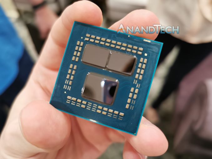
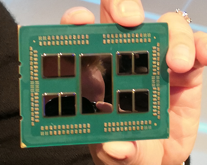
The Zen 2 design paradigm, compared to the first generation of Zen, has changed significantly. The new platform and core implementation is designed around small 8-core chiplets built on TSMC’s 7nm manufacturing process, and measure around 74-80 square millimeters. On these chiplets are two groups of four-cores arranged in a ‘core complex’, or CCX, which contains those four cores and a set of L3 cache – the L3 cache is doubled for Zen 2 over Zen 1.
Each full CPU, regardless of how many chiplets it has, is paired with a central IO die through Infinity Fabric links. The IO die acts as the central hub for all off-chip communications, as it houses all the PCIe lanes for the processor, as well as memory channels, and Infinity Fabric links to other chiplets or other CPUs. The IO die for the EPYC Rome processors is built on Global Foundries' 14nm process, however the consumer processor IO dies (which are smaller and contain fewer features) are built on the Global Foundries 12nm process.
The consumer processors, known as ‘Matisse’ or Ryzen 3rd Gen or Ryzen 3000-series, will be offered with up to two chiplets for sixteen cores. AMD is launching six versions of Matisse on July 7th, from six cores to sixteen cores. The six and eight-core processors have one chiplet, while above this the parts will have two chiplets, but in all cases the IO die is the same. This means that every Zen 2 based Ryzen 3000 processor will have access to 24 PCIe 4.0 lanes and dual channel memory. Based on the announcements today, the prices will range from $199 for the Ryzen 5 3600, up to $700+ for the sixteen core (we’re waiting on final confirmation of this price).
The EPYC Rome processors, built on these Zen 2 chiplets, will have up to eight of them, enabling a platform that can support up to 64 cores. As with the consumer processors, no chiplet can communicate directly with each other – each chiplet will only connect directly to the central IO die. That IO die houses links for eight memory channels, and up to 128 lanes of PCIe 4.0 connectivity.
AMD’s Roadmap
Before diving into the new product line, it is worth recapping where we currently sit in AMD’s planned roadmap.
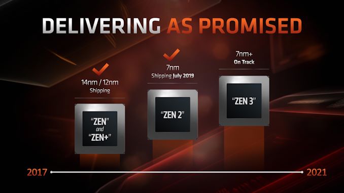
In previous roadmaps, showcasing AMD’s movement from Zen to Zen 2 and Zen 3, the company has explained that this multi-year structure will showcase Zen in 2017, Zen 2 in 2019, and Zen 3 by 2021. The cadence isn’t exactly a year, as it has depended on AMD’s design and manufacturing abilities, as well as agreements with its partners in the foundries and the current market forces.
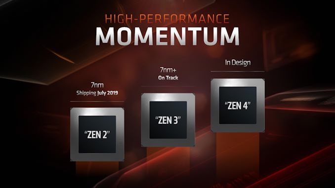
AMD has stated that its plan for Zen 2 was to always launch on 7nm, which ended up being TSMC’s 7nm (Global Foundries wasn’t going to be ready in time for 7nm, and ultimately pulled the plug). The next generation Zen 3 is expected to align with an updated 7nm process, and at this point AMD has not made any comment about a potential ‘Zen 2+’ design in the works, although at this point we do not expect to see one.
Beyond Zen 3, AMD has already stated that Zen 4 and Zen 5 are currently in various levels of their respective design stages, although the company has not committed to particular time frames or process node technologies. AMD has stated in the past that the paradigms of these platforms and processor designs are being set 3-5 years in advance, and the company states it has to make big bets every generation to ensure it can remain competitive.
For a small insight into Zen 4, in an interview with Forrest Norrod, SVP of AMD’s Enterprise, Embedded, and Semi-Custom group, at Computex, he exclusively revealed to AnandTech the code name of AMD’s Zen 4 EPYC processor: Genoa.
| AMD EPYC CPU Codenames | |||
| Gen | Year | Name | Cores |
| 1st | 2017 | Naples | 32 x Zen 1 |
| 2nd | 2019 | Rome | 64 x Zen 2 |
| 3rd | 2020 | Milan | ? x Zen 3 |
| 4th | ? | Genoa | ? x Zen 4 |
| 5th | ? | ? | ? x Zen 5 |
Forrest explained that the Zen 5 code name follows a similar pattern, but would not comment on the time frame for the Zen 4 product. Given that the Zen 3 design is expected mid-2020, that would put a Zen 4 product for late 2021/early 2022, if AMD follows its cadence. How this will play into AMD’s consumer roadmap plans is unclear at this point, and will depend on how AMD approaches its chiplet paradigm and any future adjustments to its packaging technology in order to enable further performance improvements.
Performance Claims of Zen 2
At Computex, AMD announced that it had designed Zen 2 to offer a direct +15% raw performance gain over its Zen+ platform when comparing two processors at the same frequency. At the same time, AMD also claims that at the same power, Zen 2 will offer greater than a >1.25x performance gain at the same power, or up to half power at the same performance. Combining this together, for select benchmarks, AMD is claiming a +75% performance per watt gain over its previous generation product, and a +45% performance per watt gain over its competition.
These are numbers we can’t verify at this point, as we do not have the products in hand, and when we do the embargo for benchmarking results will lift on July 7th. AMD did spend a good amount of time going through the new changes in the microarchitecture for Zen 2, as well as platform level changes, in order to show how the product has improved over the previous generation.
It should also be noted that at multiple times during AMD’s recent Tech Day, the company stated that they are not interested in going back-and-forth with its primary competition on incremental updates to try and beat one another, which might result in holding technology back. AMD is committed, according to its executives, to pushing the envelope of performance as much as it can every generation, regardless of the competition. Both CEO Dr. Lisa Su, and CTO Mark Papermaster, have said that they expected the timeline of the launch of their Zen 2 portfolio to intersect with a very competitive Intel 10nm product line. Despite this not being the case, the AMD executives stated they are still pushing ahead with their roadmap as planned.
| AMD 'Matisse' Ryzen 3000 Series CPUs | |||||||||||
| AnandTech | Cores Threads |
Base Freq |
Boost Freq |
L2 Cache |
L3 Cache |
PCIe 4.0 |
DDR4 | TDP | Price (SEP) |
||
| Ryzen 9 | 3950X | 16C | 32T | 3.5 | 4.7 | 8 MB | 64 MB | 16+4+4 | 3200 | 105W | $749 |
| Ryzen 9 | 3900X | 12C | 24T | 3.8 | 4.6 | 6 MB | 64 MB | 16+4+4 | 3200 | 105W | $499 |
| Ryzen 7 | 3800X | 8C | 16T | 3.9 | 4.5 | 4 MB | 32 MB | 16+4+4 | 3200 | 105W | $399 |
| Ryzen 7 | 3700X | 8C | 16T | 3.6 | 4.4 | 4 MB | 32 MB | 16+4+4 | 3200 | 65W | $329 |
| Ryzen 5 | 3600X | 6C | 12T | 3.8 | 4.4 | 3 MB | 32 MB | 16+4+4 | 3200 | 95W | $249 |
| Ryzen 5 | 3600 | 6C | 12T | 3.6 | 4.2 | 3 MB | 32 MB | 16+4+4 | 3200 | 65W | $199 |
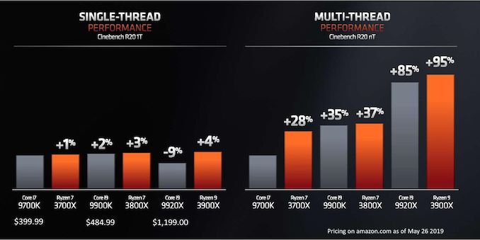
AMD’s benchmark of choice, when showcasing the performance of its upcoming Matisse processors is Cinebench. Cinebench a floating point benchmark which the company has historically done very well on, and tends to probe the CPU FP performance as well as cache performance, although it ends up often not involving much of the memory subsystem.
Back at CES 2019 in January, AMD showed an un-named 8-core Zen 2 processor against Intel’s high-end 8-core processor, the i9-9900K, on Cinebench R15, where the systems scored about the same result, but with the AMD full system consuming around 1/3 or more less power. For Computex in May, AMD disclosed a lot of the eight and twelve-core details, along with how these chips compare in single and multi-threaded Cinebench R20 results.
AMD is stating that its new processors, when comparing across core counts, offer better single thread performance, better multi-thread performance, at a lower power and a much lower price point when it comes to CPU benchmarks.
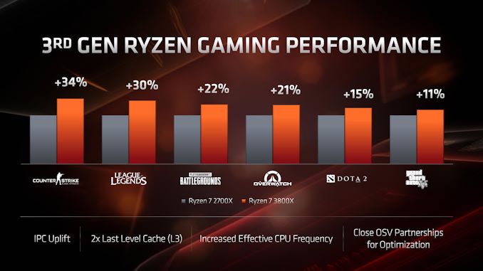
When it comes to gaming, AMD is rather bullish on this front. At 1080p, comparing the Ryzen 7 2700X to the Ryzen 7 3800X, AMD is expecting anywhere from a +11% to a +34% increase in frame rates generation to generation.
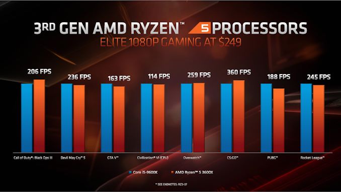
When it comes to comparing gaming between AMD and Intel processors, AMD stuck to 1080p testing of popular titles, again comparing similar processors for core counts and pricing. In pretty much every comparison, it was a back and forth between the AMD product and the Intel product – AMD would win some, loses some, or draws in others. Here’s the $250 comparison as an example:
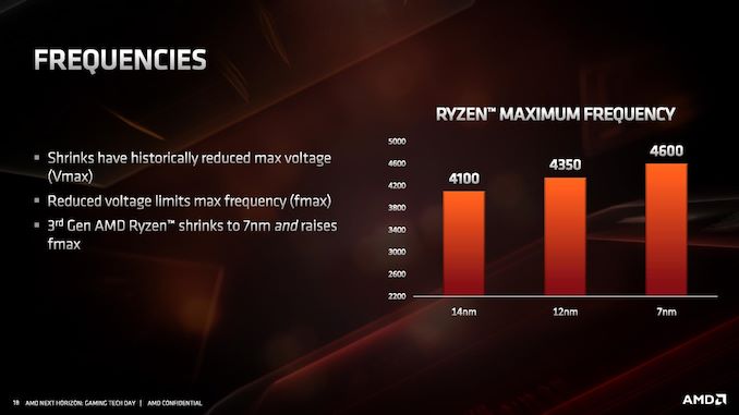
Performance in gaming in this case was designed to showcase the frequency and IPC improvements, rather than any benefits from PCIe 4.0. On the frequency side, AMD stated that despite the 7nm die shrink and higher resistivity of the pathways, they were able to extract a higher frequency out of the 7nm TSMC process compared to 14nm and 12nm from Global Foundries.
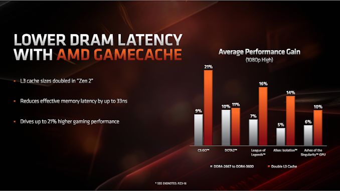
AMD also made commentary about the new L3 cache design, as it moves from 2 MB/core to 4 MB/core. Doubling the L3 cache, according to AMD, affords an additional +11% to +21% increase in performance at 1080p for gaming with a discrete GPU.
There are some new instructions on Zen 2 that would be able to assist in verifying these numbers.
Windows Optimizations
One of the key points that have been a pain in the side of non-Intel processors using Windows has been the optimizations and scheduler arrangements in the operating system. We’ve seen in the past how Windows has not been kind to non-Intel microarchitecture layouts, such as AMD’s previous module design in Bulldozer, the Qualcomm hybrid CPU strategy with Windows on Snapdragon, and more recently with multi-die arrangements on Threadripper that introduce different memory latency domains into consumer computing.
Obviously AMD has a close relationship with Microsoft when it comes down to identifying a non-regular core topology with a processor, and the two companies work towards ensuring that thread and memory assignments, absent of program driven direction, attempt to make the most out of the system. With the May 10th update to Windows, some additional features have been put in place to get the most out of the upcoming Zen 2 microarchitecture and Ryzen 3000 silicon layouts.
The optimizations come on two fronts, both of which are reasonably easy to explain.
Thread Grouping
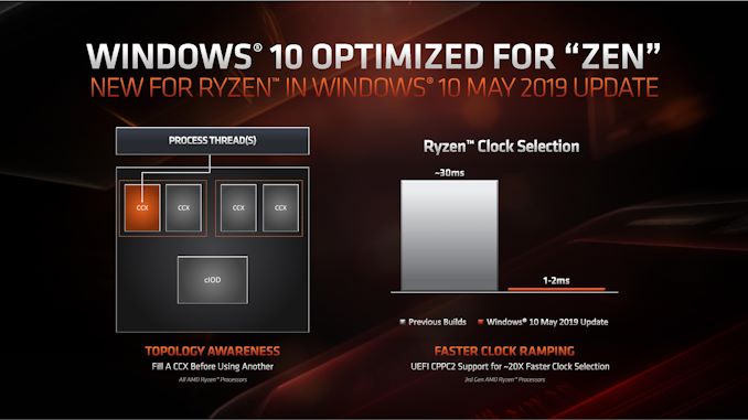
The first is thread allocation. When a processor has different ‘groups’ of CPU cores, there are different ways in which threads are allocated, all of which have pros and cons. The two extremes for thread allocation come down to thread grouping and thread expansion.
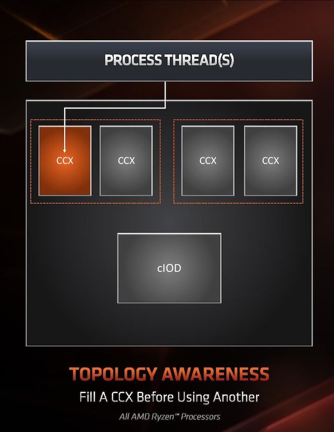
Thread grouping is where as new threads are spawned, they will be allocated onto cores directly next to cores that already have threads. This keeps the threads close together, for thread-to-thread communication, however it can create regions of high power density, especially when there are many cores on the processor but only a couple are active.
Thread expansion is where cores are placed as far away from each other as possible. In AMD’s case, this would mean a second thread spawning on a different chiplet, or a different core complex/CCX, as far away as possible. This allows the CPU to maintain high performance by not having regions of high power density, typically providing the best turbo performance across multiple threads.
The danger of thread expansion is when a program spawns two threads that end up on different sides of the CPU. In Threadripper, this could even mean that the second thread was on a part of the CPU that had a long memory latency, causing an imbalance in the potential performance between the two threads, even though the cores those threads were on would have been at the higher turbo frequency.
Because of how modern software, and in particular video games, are now spawning multiple threads rather than relying on a single thread, and those threads need to talk to each other, AMD is moving from a hybrid thread expansion technique to a thread grouping technique. This means that one CCX will fill up with threads before another CCX is even accessed. AMD believes that despite the potential for high power density within a chiplet, while the other might be inactive, is still worth it for overall performance.
For Matisse, this should afford a nice improvement for limited thread scenarios, and on the face of the technology, gaming. It will be interesting to see how much of an affect this has on the upcoming EPYC Rome CPUs or future Threadripper designs. The single benchmark AMD provided in its explanation was Rocket League at 1080p Low, which reported a +15% frame rate gain.
Clock Ramping
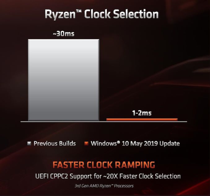
For any of our users familiar with our Skylake microarchitecture deep dive, you may remember that Intel introduced a new feature called Speed Shift that enabled the processor to adjust between different P-states more freely, as well as ramping from idle to load very quickly – from 100 ms to 40ms in the first version in Skylake, then down to 15 ms with Kaby Lake. It did this by handing P-state control back from the OS to the processor, which reacted based on instruction throughput and request. With Zen 2, AMD is now enabling the same feature.
AMD already has sufficiently more granularity in its frequency adjustments over Intel, allowing for 25 MHz differences rather than 100 MHz differences, however enabling a faster ramp-to-load frequency jump is going to help AMD when it comes to very burst-driven workloads, such as WebXPRT (Intel’s favorite for this sort of demonstration). According to AMD, the way that this has been implemented with Zen 2 will require BIOS updates as well as moving to the Windows May 10th update, but it will reduce frequency ramping from ~30 milliseconds on Zen to ~1-2 milliseconds on Zen 2. It should be noted that this is much faster than the numbers Intel tends to provide.
The technical name for AMD’s implementation involves CPPC2, or Collaborative Power Performance Control 2, and AMD’s metrics state that this can increase burst workloads and also application loading. AMD cites a +6% performance gain in application launch times using PCMark10’s app launch sub-test.
Hardened Security for Zen 2
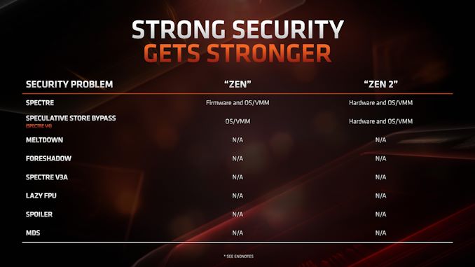
Another aspect to Zen 2 is AMD’s approach to heightened security requirements of modern processors. As has been reported, a good number of the recent array of side channel exploits do not affect AMD processors, primarily because of how AMD manages its TLB buffers that have always required additional security checks before most of this became an issue. Nonetheless, for the issues to which AMD is vulnerable, it has implemented a full hardware-based security platform for them.
The change here comes for the Speculative Store Bypass, known as Spectre v4, which AMD now has additional hardware to work in conjunction with the OS or virtual memory managers such as hypervisors in order to control. AMD doesn’t expect any performance change from these updates. Newer issues such as Foreshadow and Zombieload do not affect AMD processors.
New Instructions
Cache and Memory Bandwidth QoS Control
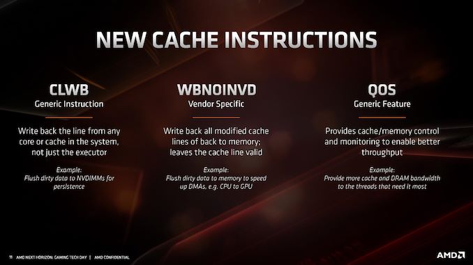
As with most new x86 microarchitectures, there is a drive to increase performance through new instructions, but also try for parity between different vendors in what instructions are supported. For Zen 2, while AMD is not catering to some of the more exotic instruction sets that Intel might do, it is adding in new instructions in three different areas.
The first one, CLWB, has been seen before from Intel processors in relation to non-volatile memory. This instruction allows the program to push data back into the non-volatile memory, just in case the system receives a halting command and data might be lost. There are other instructions associated with securing data to non-volatile memory systems, although this wasn’t explicitly commented on by AMD. It could be an indication that AMD is looking to better support non-volatile memory hardware and structures in future designs, particularly in its EPYC processors.
The second cache instruction, WBNOINVD, is an AMD-only command, but builds on other similar commands such as WBINVD. This command is designed to predict when particular parts of the cache might be needed in the future, and clears them up ready in order to accelerate future calculations. In the event that the cache line needed isn’t ready, a flush command would be processed in advance of the needed operation, increasing latency – by running a cache line flush in advance while the latency-critical instruction is still coming down the pipe helps accelerate its ultimate execution.
The final set of instructions, filed under QoS, actually relates to how cache and memory priorities are assigned.
When a cloud CPU is split into different containers or VMs for different customers, the level of performance is not always consistent as performance could be limited based on what another VM is doing on the system. This is known as the ‘noisy neighbor’ issue: if someone else is eating all the core-to-memory bandwidth, or L3 cache, it can be very difficult for another VM on the system to have access to what it needs. As a result of that noisy neighbor, the other VM will have a highly variable latency on how it can process its workload. Alternatively, if a mission critical VM is on a system and another VM keeps asking for resources, the mission critical one might end up missing its targets as it doesn’t have all the resources it needs access to.
Dealing with noisy neighbors, beyond ensuring full access to the hardware as a single user, is difficult. Most cloud providers and operations won’t even tell you if you have any neighbors, and in the event of live VM migration, those neighbors might change very frequently, so there is no guarantee of sustained performance at any time. This is where a set of dedicated QoS (Quality of Service) instructions come in.
As with Intel’s implementation, when a series of VMs is allocated onto a system on top of a hypervisor, the hypervisor can control how much memory bandwidth and cache that each VM has access to. If a mission critical 8-core VM requires access to 64 MB of L3 and at least 30 GB/s of memory bandwidth, the hypervisor can control that the priority VM will always have access to that amount, and either eliminate it entirely from the pool for other VMs, or intelligently restrict the requirements as the mission critical VM bursts into full access.
Intel only enables this feature on its Xeon Scalable processors, however AMD will enable it up and down its Zen 2 processor family range, for consumers and enterprise users.
The immediate issue I had with this feature is on the consumer side. Imagine if a video game demands access to all the cache and all the memory bandwidth, while some streaming software would get access to none – it could cause havoc on the system. AMD explained that while technically individual programs can request a certain level of QoS, however it will be up to the OS or the hypervisor to control if those requests are both valid and suitable. They see this feature more as an enterprise feature used when hypervisors are in play, rather than bare metal installations on consumer systems.
CCX Size
Moving down in node size brings up a number of challenges in the core and beyond. Even disregarding power and frequency, the ability to put structures into silicon and then integrate that silicon into the package, as well as providing power to the right parts of the silicon through the right connections becomes an exercise in itself. AMD gave us some insight into how 7nm changed some of its designs, as well as the packaging challenges therein.
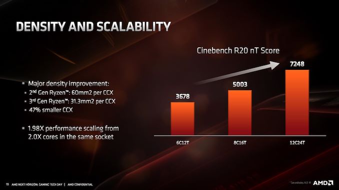
A key metric given up by AMD relates to the core complex: four cores, the associated core structures, and then L2 and L3 caches. With 12nm and the Zen+ core, AMD stated that a single core complex was ~60 square millimeters, which separates into 44mm2 for the cores and 16mm2 for the 8MB of L3 per CCX. Add two of these 60mm2 complexes with a memory controller, PCIe lanes, four IF links, and other IO, and a Zen+ zeppelin die was 213 mm2 in total.
For Zen 2, a single chiplet is 74mm2, of which 31.3 mm2 is a core complex with 16 MB of L3. AMD did not breakdown this 31.3 number into cores and L3, but one might imagine that the L3 might be approaching 50% of that number. The reason the chiplet is so much smaller is that it doesn’t need memory controllers, it only has one IF link, and has no IO, because all of the platform requirements are on the IO die. This allows AMD to make the chiplets extremely compact. However if AMD intends to keep increasing the L3 cache, we might end up with most of the chip as L3.
Overall however, AMD has stated that the CCX (cores plus L3) has decreased in size by 47%. That is showing great scaling, especially if the +15% raw instruction throughput and increased frequency comes into play. Performance per mm2 is going to be a very exciting metric.
Packaging
With Matisse staying in the AM4 socket, and Rome in the EPYC socket, AMD stated that they had to make some bets on its packaging technology in order to maintain compatibility. Invariably some of these bets end up being tradeoffs for continual support, however AMD believes that the extra effort has been worth the continued compatibility.
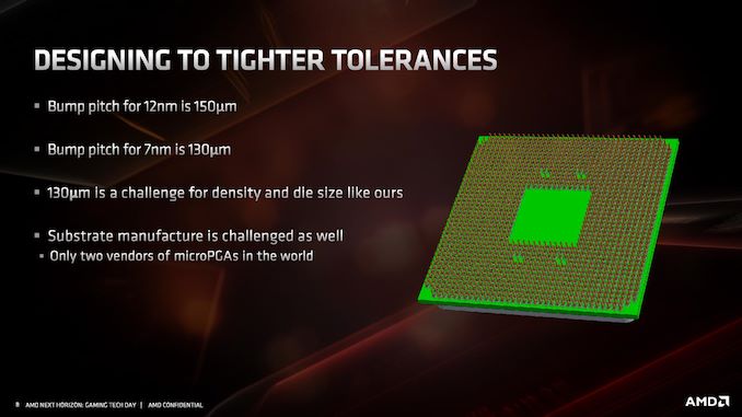
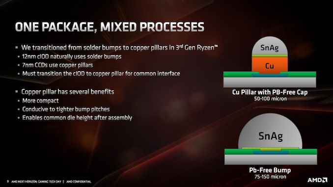
One of the key points AMD spoke about with relation to packaging is how each of the silicon dies are attached to the package. In order to enable a pin-grid array desktop processor, the silicon has to be affixed to the processor in a BGA fashion. AMD stated that due to the 7nm process, the bump pitch (the distance between the solder balls on the silicon die and package) reduced from 150 microns on 12nm to 130 microns on 7nm. This doesn’t sound like much, however AMD stated that there are only two vendors in the world with technology sufficient to do this. The only alternative would be to have a bigger bit of silicon to support a larger bump pitch, ultimately leading to a lot of empty silicon (or a different design paradigm).
One of the ways in order to enable the tighter bump pitch is to adjust how the bumps are processed on the underside of the die. Normally a solder bump on a package is a blob/ball of lead-free solder, relying on the physics of surface tension and reflow to ensure it is consistent and regular. In order to enable the tighter bump pitches however, AMD had to move to a copper pillar solder bump topology.
In order to enable this feature, copper is epitaxially deposited within a mask in order to create a ‘stand’ on which the reflow solder sits. Due to the diameter of the pillar, less solder mask is needed and it creates a smaller solder radius. AMD also came across another issue, due to its dual die design inside Matisse: if the IO die uses standard solder bump masks, and the chiplets use copper pillars, there needs to be a level of height consistency for integrated heat spreaders. For the smaller copper pillars, this means managing the level of copper pillar growth.
AMD explained that it was actually easier to manage this connection implementation than it would be to build different height heatspreaders, as the stamping process used for heatspreaders would not enable such a low tolerance. AMD expects all of its 7nm designs in the future to use the copper pillar implementation.
Routing
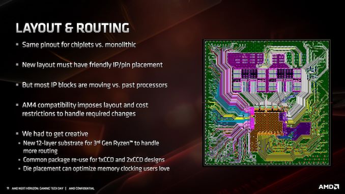
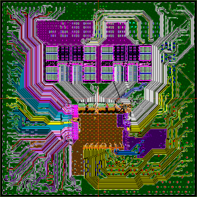
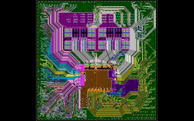
Beyond just putting the silicon onto the organic substrate, that substrate has to manage connections between the die and externally to the die. AMD had to increase the number of substrate layers in the package to 12 for Matisse in order to handle the extra routing (no word on how many layers are required in Rome, perhaps 14). This also becomes somewhat complicated for single core chiplet and dual core chiplet processors, especially when testing the silicon before placing it onto the package.
From the diagram we can clearly see the IF links from the two chiplets going to the IO die, with the IO die also handling the memory controllers and what looks like power plane duties as well. There are no in-package links between the chiplets, in case anyone was still wondering: the chiplets have no way of direct communication – all communication between chiplets is handled through the IO die.
AMD stated that with this layout they also had to be mindful of how the processor was placed in the system, as well as cooling and memory layout. Also, when it comes to faster memory support, or the tighter tolerances of PCIe 4.0, all of this also needs to be taken into consideration as provide the optimal path for signaling without interference from other traces and other routing.
AMD Zen 2 Microarchitecture Overview
The Quick Analysis
At AMD’s Tech Day, on hand was Fellow and Chief Architect Mike Clark to go through the changes. Mike is a great engineer to talk to, although what always amuses me (for any company, not just AMD) is that engineers that talk about the latest products coming to market are already working one, two, or three generations ahead at the company. Mike remarked that it took him a while to think back to the specific Zen+ to Zen 2 changes, while his mind internally is already several generations down the line.
An interesting element to Zen 2 is around the intention. Initially Zen 2 was merely going to be a die shrink of Zen+, going from 12nm down to 7nm, similar to what we used to see with Intel in its tick-tock model for the initial part of the century. However, based on internal analysis and the time frame for 7nm, it was decided that Zen 2 would be used as a platform for better performance, taking advantage of 7nm in multiple ways rather than just redesigning the same layout on a new process node. As a result of the adjustments, AMD is promoting a +15% IPC improvement for Zen 2 over Zen+.
When it comes down to the exact changes in the microarchitecture, what we’re fundamentally looking at is still a similar floorplan to what Zen looks like. Zen 2 is a family member of the Zen family, and not a complete redesign or different paradigm on how to process x86 – as will other architectures that have familial updates, Zen 2 affords a more efficient core and a wider core, allowing better instruction throughput.
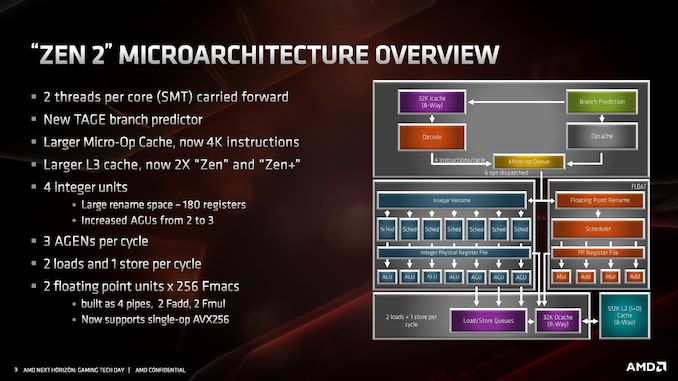
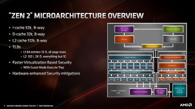
At a high level, the core looks very much the same. Highlights of the Zen 2 design include a different L2 branch predictor known as a TAGE predictor, a doubling of the micro-op cache, a doubling of the L3 cache, an increase in integer resources, an increase in load/store resources, and support for single-operation AVX-256 (or AVX2). AMD has stated that there is no frequency penalty for AVX2, based on its energy aware frequency platform.
AMD has also made adjustments to the cache system, the most notable being for the L1 instruction cache, which has been halved to 32 kB, but associativity has doubled. This change was made for important reasons, which we’ll go into over the next pages. The L1 data cache and L2 caches are unchanged, however the translation lookaside buffers (TLBs) have increased support. AMD also states that it has added deeper virtualization support with respect to security, helping enable features further down the pipeline. As mentioned previously in this article, there are also security hardening updates.
For the quick analysis, it’s easy to tell that doubling the micro-op cache is going to offer a significant improvement to IPC in a number of scenarios, and combine that with an increase in load/store resources is going to help more instructions get pushed through. The double L3 cache is going to help in specific workloads, as would the AVX2 single-op support, but the improved branch predictor is also going to showcase raw performance uplift. All-in-all, for an on-paper analysis, AMD’s +15% IPC improvement seems like a very reasonable number to promote.
Over the next few pages, we’ll go deeper into how the microarchitecture has changed.
Fetch/Prefetch
Starting with the front end of the processor, the prefetchers.
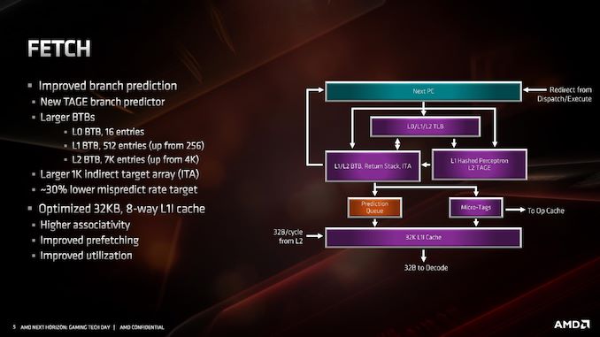
AMD’s primary advertised improvement here is the use of a TAGE predictor, although it is only used for non-L1 fetches. This might not sound too impressive: AMD is still using a hashed perceptron prefetch engine for L1 fetches, which is going to be as many fetches as possible, but the TAGE L2 branch predictor uses additional tagging to enable longer branch histories for better prediction pathways. This becomes more important for the L2 prefetches and beyond, with the hashed perceptron preferred for short prefetches in the L1 based on power.
In the front end we also get larger BTBs, to help keep track of instruction branches and cache requests. The L1 BTB has doubled in size from 256 entry to 512 entry, and the L2 is almost doubled to 7K from 4K. The L0 BTB stays at 16 entries, but the Indirect target array goes up to 1K entries. Overall, these changes according to AMD affords a 30% lower mispredict rate, saving power.
One other major change is the L1 instruction cache. We noted that it is smaller for Zen 2: only 32 KB rather than 64 KB, however the associativity has doubled, from 4-way to 8-way. Given the way a cache works, these two effects ultimately don’t cancel each other out, however the 32 KB L1-I cache should be more power efficient, and experience higher utilization. The L1-I cache hasn’t just decreased in isolation – one of the benefits of reducing the size of the I-cache is that it has allowed AMD to double the size of the micro-op cache. These two structures are next to each other inside the core, and so even at 7nm we have an instance of space limitations causing a trade-off between structures within a core. AMD stated that this configuration, the smaller L1 with the larger micro-op cache, ended up being better in more of the scenarios it tested.
Decode
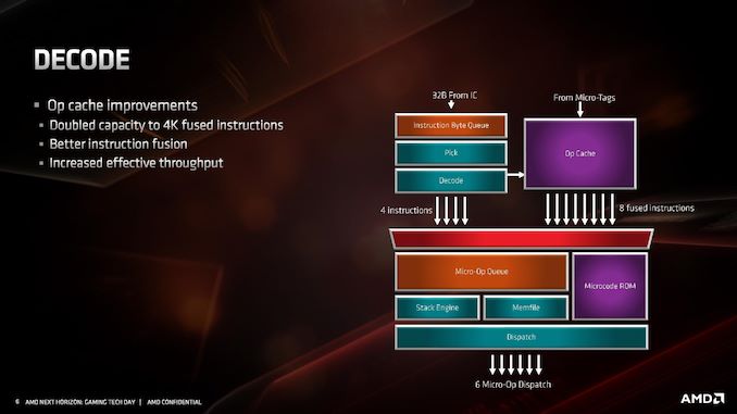
For the decode stage, the main uptick here is the micro-op cache. By doubling in size from 2K entry to 4K entry, it will hold more decoded operations than before, which means it should experience a lot of reuse. In order to facilitate that use, AMD has increased the dispatch rate from the micro-op cache into the buffers up to 8 fused instructions. Assuming that AMD can bypass its decoders often, this should be a very efficient block of silicon.
What makes the 4K entry more impressive is when we compare it to the competition. In Intel’s Skylake family, the micro-op cache in those cores are only 1.5K entry. Intel increased the size by 50% for Ice Lake to 2.25K, but that core is coming to mobile platforms later this year and perhaps to servers next year. By comparison AMD’s Zen 2 core will cover the gamut from consumer to enterprise. Also at this time we can compare it to Arm’s A77 CPU micro-op cache, which is 1.5K entry, however that cache is Arm’s first micro-op cache design for a core.
The decoders in Zen 2 stay the same, we still have access to four complex decoders (compared to Intel’s 1 complex + 4 simple decoders), and decoded instructions are cached into the micro-op cache as well as dispatched into the micro-op queue.
AMD has also stated that it has improved its micro-op fusion algorithm, although did not go into detail as to how this affects performance. Current micro-op fusion conversion is already pretty good, so it would be interesting to see what AMD have done here. Compared to Zen and Zen+, based on the support for AVX2, it does mean that the decoder doesn’t need to crack an AVX2 instruction into two micro-ops: AVX2 is now a single micro-op through the pipeline.
Going beyond the decoders, the micro-op queue and dispatch can feed six micro-ops per cycle into the schedulers. This is slightly imbalanced however, as AMD has independent integer and floating point schedulers: the integer scheduler can accept six micro-ops per cycle, whereas the floating point scheduler can only accept four. The dispatch can simultaneously send micro-ops to both at the same time however.
Floating Point
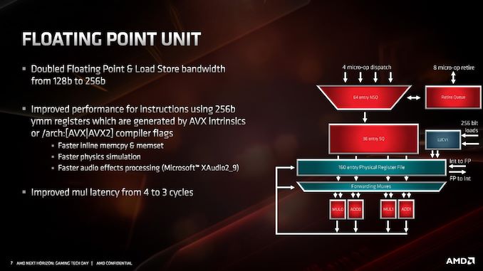
The key highlight improvement for floating point performance is full AVX2 support. AMD has increased the execution unit width from 128-bit to 256-bit, allowing for single-cycle AVX2 calculations, rather than cracking the calculation into two instructions and two cycles. This is enhanced by giving 256-bit loads and stores, so the FMA units can be continuously fed. AMD states that due to its energy aware scheduling, there is no predefined frequency drop when using AVX2 instructions (however frequency may be reduced dependent on temperature and voltage requirements, but that’s automatic regardless of instructions used)
In the floating point unit, the queues accept up to four micro-ops per cycle from the dispatch unit which feed into a 160-entry physical register file. This moves into four execution units, which can be fed with 256b data in the load and store mechanism.
Other tweaks have been made to the FMA units than beyond doubling the size – AMD states that they have increased raw performance in memory allocations, for repetitive physics calculations, and certain audio processing techniques.
Another key update is decreasing the FP multiplication latency from 4 cycles to 3 cycles. That is quite a significant improvement. AMD has stated that it is keeping a lot of the detail under wraps, as it wants to present it at Hot Chips is August. We’ll be running a full instruction analysis for our reviews on July 7th.
Integer Units, Load and Store
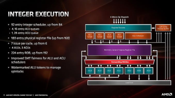
The integer unit schedulers can accept up to six micro-ops per cycle, which feed into the 224-entry reorder buffer (up from 192). The Integer unit technically has seven execution ports, comprised of four ALUs (arithmetic logic units) and three AGUs (address generation units).
The schedulers comprise of four 16-entry ALU queues and one 28-entry AGU queue, although the AGU unit can feed 3 micro-ops per cycle into the register file. The AGU queue has increased in size based on AMD’s simulations of instruction distributions in common software. These queues feed into the 180-entry general purpose register file (up from 168), but also keep track of specific ALU operations to prevent potential halting operations.
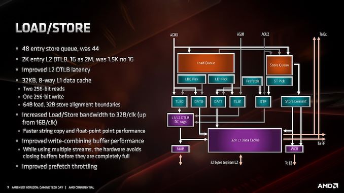
The three AGUs feed into the load/store unit that can support two 256-bit reads and one 256-bit write per cycle. Not all the three AGUs are equal, judging by the diagram above: AGU2 can only manage stores, whereas AGU0 and AGU1 can do both loads and stores.
The store queue has increased from 44 to 48 entries, and the TLBs for the data cache have also increased. The key metric here though is the load/store bandwidth, as the core can now support 32 bytes per clock, up from 16.
Cache and Infinity Fabric
If it hasn’t been hammered in already, the big change in the cache is the L1 instruction cache which has been reduced from 64 KB to 32 KB, but the associativity has increased from 4-way to 8-way. This change enabled AMD to increase the size of the micro-op cache from 2K entry to 4K entry, and AMD felt that this gave a better performance balance with how modern workloads are evolving.
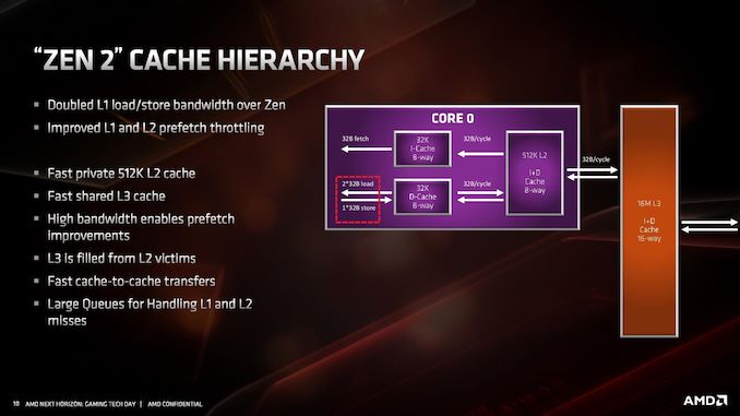
The L1-D cache is still 32KB 8-way, while the L2 cache is still 512KB 8-way. The L3 cache, which is a non-inclusive cache (compared to the L2 inclusive cache), has now doubled in size to 16 MB per core complex, up from 8 MB. AMD manages its L3 by sharing a 16MB block per CCX, rather than enabling access to any L3 from any core.
Because of the increase in size of the L3, latency has increased slightly. L1 is still 4-cycle, L2 is still 12-cycle, but L3 has increased from ~35 cycle to ~40 cycle (this is a characteristic of larger caches, they end up being slightly slower latency; it’s an interesting trade off to measure). AMD has stated that it has increased the size of the queues handling L1 and L2 misses, although hasn’t elaborated as to how big they now are.
Infinity Fabric
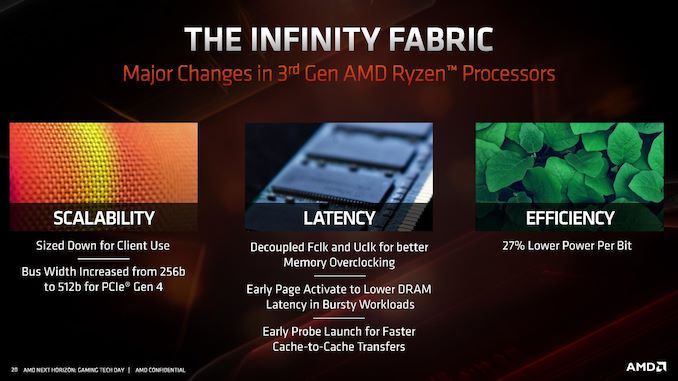
With the move to Zen 2, we also move to the second generation of Infinity Fabric. One of the major updates with IF2 is the support of PCIe 4.0, and thus the increase of the bus width from 256-bit to 512-bit.
Overall efficiency of IF2 has improved 27% according to AMD, leading to a lower power per bit. As we move to more IF links in EPYC, this will become very important as data is transferred from chiplet to IO die.
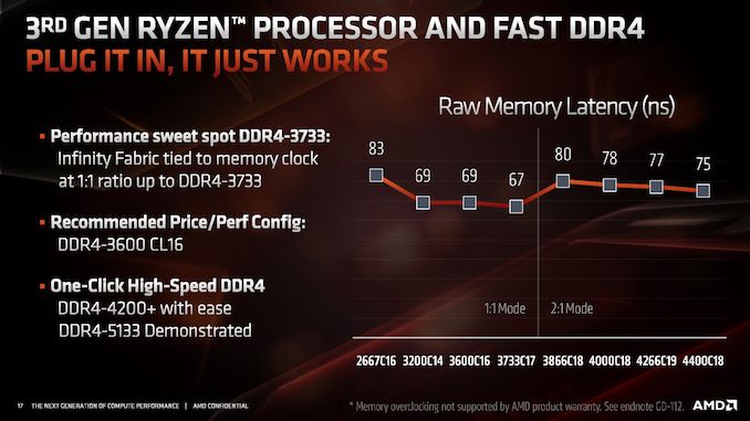
One of the features of IF2 is that the clock has been decoupled from the main DRAM clock. In Zen and Zen+, the IF frequency was coupled to the DRAM frequency, which led to some interesting scenarios where the memory could go a lot faster but the limitations in the IF meant that they were both limited by the lock-step nature of the clock. For Zen 2, AMD has introduced ratios to the IF2, enabling a 1:1 normal ratio or a 2:1 ratio that reduces the IF2 clock in half.
This ratio should automatically come into play around DDR4-3600 or DDR4-3800, but it does mean that IF2 clock does reduce in half, which has a knock on effect with respect to bandwidth. It should be noted that even if the DRAM frequency is high, having a slower IF frequency will likely limit the raw performance gain from that faster memory. AMD recommends keeping the ratio at a 1:1 around DDR4-3600, and instead optimizing sub-timings at that speed.
Building a core like Zen 2 requires more than just building a core. The interplay between the core, the SoC design, and then the platform requires different internal teams to come together to create a level of synergy that working separately lacks. What AMD has done with the chiplet design and Zen 2 shows great promise, not only in taking advantage of smaller process nodes, but also driving one path on the future of compute.
When going down a process node, the main advantages are lower power. That can be taken in a few ways: lower power for operation at the same performance, or more power budget to do more. We see this with core designs over time: as more power budget is opened or different units within the core get more efficient, that extra power is used to drive cores wider, hopefully increasing raw instruction rate. It’s not an easy equation to solve, as there are many trade-offs: one such example in the Zen 2 core is the relationship between the reduced L1 I-cache that has allowed AMD to double the micro-op cache, which overall AMD expects to help with performance and power. Going into the minutae of what might be possible, at least at a high level, is like playing with Lego for these engineers.
All that being said, Zen 2 looks a lot like Zen. It is part of the same family, which means it looks very similar. What AMD has done with the platform, enabling PCIe 4.0, and putting the design in place to rid the server processors of the NUMA-like environment is going to help AMD in the long run. The outlook is good for AMD here, depending on how high it can drive the frequency of the server parts, but Zen 2 plus Rome is going to remove a good number of questions that customers on the fence had about Zen.
Overall AMD has quoted a +15% core performance improvement with Zen 2 over Zen+. With the core changes, at a high level, that certainly looks feasible. Users focused on performance will love the new 16-core Ryzen 9 3950X, while the processor seems nice an efficient at 105W, so it will be interesting so see what happens at lower power. We're also anticipating a very strong Rome launch here over the next few months, especially with features like double FP performance and QoS, and the raw multithreading performance of 64 cores is going to be an interesting disruptor to the market, especially if priced effectively. We’ll be getting the hardware on hand here soon to present our findings when the processors are launched on July 7th.

