Original Link: https://www.anandtech.com/show/14385/arm-announces-malig77-gpu
Arm's New Mali-G77 & Valhall GPU Architecture: A Major Leap
by Andrei Frumusanu on May 27, 2019 12:00 AM EST
Along today’s announcement of the new Cortex-A77 CPU microarchitecture, the arguably bigger announcement is Arm’s unveiling of the new Valhall GPU architecture and the new Mali-G77 GPU. It’s been three years since the unveiling of the Bifrost architecture, and as the industry and workloads continue to evolve, so must the company’s GPUs.
Valhall and the new Mali-G77 follow up on the last three generations of Mali GPUs with some significant improvements in performance, density and efficiency. While last year’s G76 introduced some large changes to the compute architecture of the execution engines, the G77 goes a lot further and departs from Arm’s relatively unusual compute core design.
A look back at Bifrost – third time’s the charm
It’s not too big of a secret that the last few years haven’t been very kind to Arm’s GPU IP offerings. When the first Bifrost GPU - the Mali-G71 was announced back in 2016 and productised later that year in the Kirin 960 and Exynos 8895, we had expected good performance and efficiency gains.
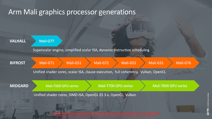
Bifrost was Arm’s first scalar GPU architecture, departing from the previous generation’s (Midgard: T-600, 700 & 800 series) vector instruction design. The change was fundamental and akin to what we saw desktop GPU vendors like AMD and Nvidia introduce with their new GCN and Tesla architectures last decade.
Unfortunately the first two generations of Bifrost, the Mali-G71 and subsequent G72 weren’t very good GPUs. Arm’s two leading licensees, HiSilicon and Samsung, both came out with quite disappointing SoCs when it came to their GPUs these two generations. The Kirin 960 and 970 in particular were extremely bad in this regard and I’d argue it had quite a lot of impact on Huawei and Honor’s product planning and marketing.
| GFXBench Manhattan 3.1 Offscreen Power Efficiency (System Active Power) |
||||
| Mfc. Process | FPS | Avg. Power (W) |
Perf/W Efficiency |
|
| iPhone XS (A12) Warm | 7FF | 76.51 | 3.79 | 20.18 fps/W |
| iPhone XS (A12) Cold / Peak | 7FF | 103.83 | 5.98 | 17.36 fps/W |
| Galaxy 10+ (Snapdragon 855) | 7FF | 70.67 | 4.88 | 14.46 fps/W |
| Galaxy 10+ (Exynos 9820) | 8LPP | 68.87 | 5.10 | 13.48 fps/W |
| Galaxy S9+ (Snapdragon 845) | 10LPP | 61.16 | 5.01 | 11.99 fps/W |
| Huawei Mate 20 Pro (Kirin 980) | 7FF | 54.54 | 4.57 | 11.93 fps/W |
| Galaxy S9 (Exynos 9810) | 10LPP | 46.04 | 4.08 | 11.28 fps/W |
| Galaxy S8 (Snapdragon 835) | 10LPE | 38.90 | 3.79 | 10.26 fps/W |
| LeEco Le Pro3 (Snapdragon 821) | 14LPP | 33.04 | 4.18 | 7.90 fps/W |
| Galaxy S7 (Snapdragon 820) | 14LPP | 30.98 | 3.98 | 7.78 fps/W |
| Huawei Mate 10 (Kirin 970) | 10FF | 37.66 | 6.33 | 5.94 fps/W |
| Galaxy S8 (Exynos 8895) | 10LPE | 42.49 | 7.35 | 5.78 fps/W |
| Galaxy S7 (Exynos 8890) | 14LPP | 29.41 | 5.95 | 4.94 fps/W |
| Meizu PRO 5 (Exynos 7420) | 14LPE | 14.45 | 3.47 | 4.16 fps/W |
| Nexus 6P (Snapdragon 810 v2.1) | 20Soc | 21.94 | 5.44 | 4.03 fps/W |
| Huawei Mate 8 (Kirin 950) | 16FF+ | 10.37 | 2.75 | 3.77 fps/W |
| Huawei Mate 9 (Kirin 960) | 16FFC | 32.49 | 8.63 | 3.77 fps/W |
| Huawei P9 (Kirin 955) | 16FF+ | 10.59 | 2.98 | 3.55 fps/W |
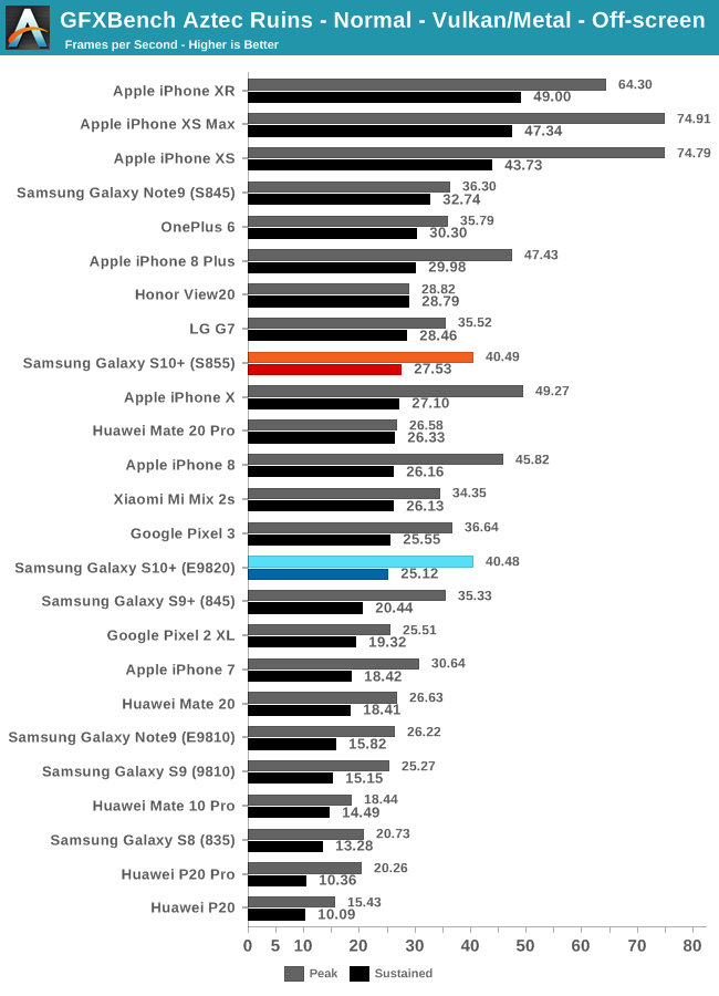
The last iteration of the Bifrost architecture, the Mali-G76 was a more significant jump for Arm and the IP was largely able to resolve some of the critical issues of its predecessors, resulting in relatively good results for the Exynos 9820 and Kirin 980 chipsets.
Unfortunately while Arm was catching up and fixing Bifrost’s issues, the competition didn’t merely hold still and was pushing the envelope. Qualcomm’s Adreno GPU architecture had been leading the mobile landscape for several years now, and even though the Adreno 640 didn’t post quite as impressive improvements this year, it’s still clearly leading Arm in terms of performance, efficiency and density. More worrisome is the fact that Apple’s GPU in the A12 was an absolutely major jump in terms of performance and efficiency, performing massively better than even Qualcomm’s best, not to speak of Arm’s own Mali GPUs.
Introducing Valhall – A major revamp
Today we’ll be covering Arm’s brand-new GPU architecture: Valhall (anglicized version of the old Norse Valhöll, a.k.a. Valhalla). The new architecture brings a brand-new ISA and compute core design that tries to address the major shortcomings of the Bifrost architecture, and looks to be a lot more similar to the design approaches we saw adopted by other GPU vendors.
The first iteration of the Valhall GPU is the new Mali-G77 which will implement all of the architectural and micro-architectural improvements we’ll be discussing today.
What’s being promised is a 30% gain in energy efficiency as well as area density (at ISO-performance & process) and a 60% increase in performance of machine learning inferencing workloads on the GPU.
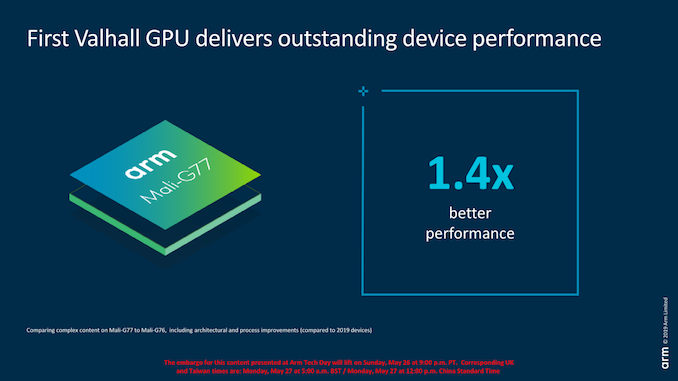
More interestingly, upcoming end-of-2019 and 2020 SoCs are projected to see a 40% increase in performance over 2019 devices. Next-generation SoCs are projected to have only minor process node improvements, so most of the gains quoted here are due to the architectural and microarchitectural leaps made by the new Mali-G77 GPU.
Introducing Valhall: A new ISA for Modern Workloads
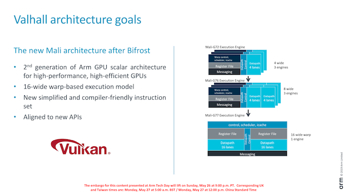
At the heart of the new Valhall architecture is Arm’s new execution core that differs significantly from its predecessor. It’s still a scalar design, however unlike Bifrost’s unusually narrow 4 and 8-wide design, the new execution core is more akin to what we see from desktop GPU vendors such as AMD and Nvidia.
Bifrost’s in its initial iterations on the Mali-G71 and G72 the execution block in the core consisted of a 4-wide scalar SIMD units and with a warp/wavefront size of also 4. On the G76 last year this was increased to two 4-wide units with a warp size of 8. Initially during the design of Bifrost, Arm’s rationale for going with such narrow units and warp sizes was to reduce the amount of idle cycles on the ALUs. Workloads back then weren’t able to efficiently fill enough threads to justify for going for larger warp design. The benefit here is that in theory Arm would have achieved better ALU utilisation at a cost of more control logic.
As new generation workloads over the years have evolved though, this approach suddenly didn’t make much sense anymore. Today’s games are quickly advancing towards more compute complexity, and in particular in the last year or two we’ve seen games ported to mobile that originated on the PC.
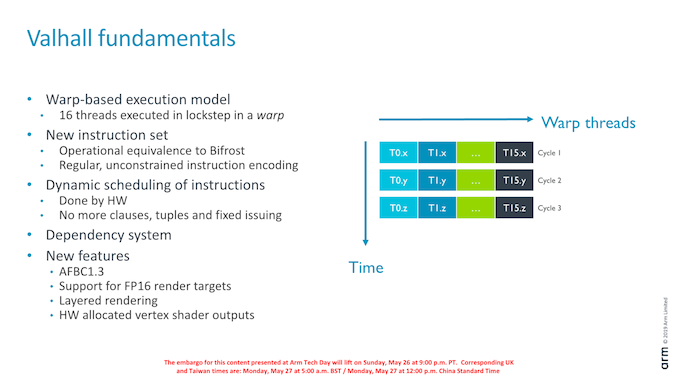
With shader compute complexity going up, it is much easier to issue more threads and justify for going to a wider warp design. In this case, the new Valhall architecture supports a 16-wide warp-based execution model. It’s still not quite as wide as Nvidia’s 32-wide or AMD’s 64-wide designs, but it’s a big leap considering that before last year Mali GPUs were working with a 4-wide warp execution model.
Arm has also changed the ISA itself and simplified a lot of the instructions. While we don’t have more details, the new ISA is said to be more compiler friendly and adapted and designed to be better aligned with modern APIs such as Vulkan.
Previous Bifrost GPUs and even Midgard GPUs before that we saw a single GPU core employ multiple execution engines. These 3 engines would have their own dedicated datapath control logic, their own scheduler and instruction caches and register file and messaging blocks, which naturally creates quite a lot of overhead transistors. Particularly on the high-end this didn’t make sense anymore as we hadn’t seen the GPU IP vary the number of execution engines since the T860/880 series 4+ years ago.
The new G77 consolidates the previous generations “small” execution engines into a single larger IP block with shared control logic. There’s still some duplication in the IP design of the new engine: the actual ALU pipelines are organised into two “clusters”, each with their own 16-wide FMA units as well as accompanying execution units.
Part of the new ISA is a new encoding which is more regular in comparison to what we saw in Bifrost. An important new feature of the Valhall architecture is that the new ISA gets rid of fixed issue scheduling, clauses and tuples. In Bifrost, Arm delegated scheduling of instructions to the compiler, grouping them in so called clauses. This worked in practice, although it put a lot of work onto the compiler to get the best results in attempting to hide latency between instructions and data accesses.
In Valhall, the scheduling is completely done by hardware, which is essentially more akin to how an out-of-order CPU works. This new design also means that the actual ISA is more disconnected from the implemented microarchitecture, a more forward-thinking design choice.
The new ISA also put a focus on optimising texturing instructions, which is linked to the new architecture’s much increased texturing capability.
Other changes include incremental updates to existing technologies and evolution of the data structures, which includes optimisations to the geometry flow and optimisations to AFBC (Arm frame-buffer compression).
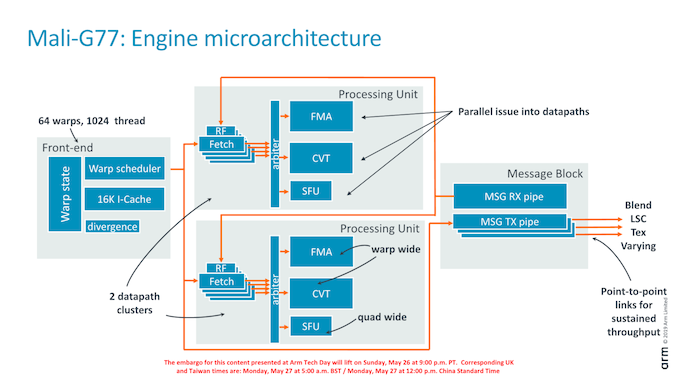
Delving deeper into the structure of the execution engine, we see that the structure can generally be grouped into four blocks: the front-end which includes the warp scheduler and I-cache, two identical datapath clusters (processing units), and the message block which connects to the load/store unit as well as the fixed-function blocks.
The front-end supports up to 64 warps or 1024 threads. The processing units each have three ALUs: the FMA and CVT (convert) units are 16-wide as the warp while the SFU (Special function unit) is 4-wide.
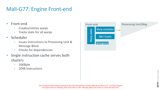
The front-end creates and retires warps and maintains the necessary state. Within the front-end there’s a dynamic scheduler which decides which instructions from each warp to execute. Warps that are waiting on a dependency are replaced with ones that are ready to execute.
The I-cache is shared among the processing and is 16KB (2048 instructions) 4-way set-associative and is able to issue 4 instructions per cycle in terms of bandwidth.
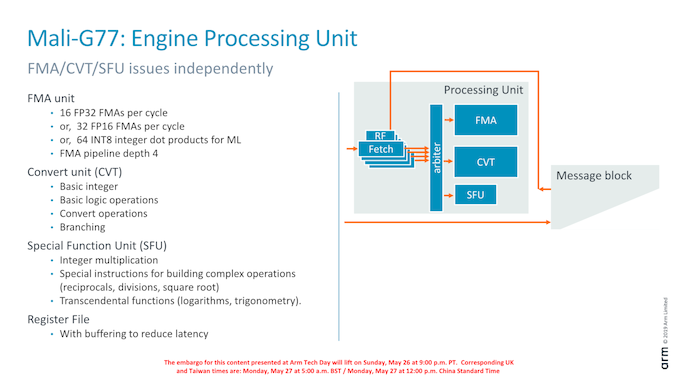
Within the actual processing units (clusters) we have four fetch units that are issuing into the arithmetic units. Each of the fetch units has a tightly coupled register file, as well as a forwarding buffer that reduces latency to access the register file.
The FMA ALU supports 16 FP32 FMA per cycle, double that for FP16 and again double that for INT8 dot-products. The convert unit handles basic integer operations and naturally type conversion operations, as well as serves as the branch port.
The SFU is 4-wide as opposed to 16-wide because it handles less frequently used instructions that don’t need quite as large throughput.
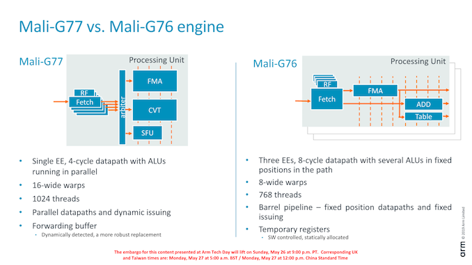
Overall in a higher-level comparison between the execution engines of the Mali-G77 versus the Mali-G76, we’re seeing one single engine versus three engines. One single engine has more instances on the primary datapath, and less instances of the control and I-cache, improving the area efficiency of the overall block.
An important change in the latency of the ALUs is that the datapath is now 4-cycles deep as opposed to 8-cycles previously which improves performance whenever one doesn’t chain operations.
Again, the new core has a superscalar-like issuing as opposed to the barrel pipeline design of the past where the pipeline had to make due with the aforementioned latency compromises. This change is also part of why the new compiler is much simplified as it no longer has to find matching instructions to issue simultaneously, as previously on the old pipeline design.
The Mali-G77 Microarchitecture
Having covered the execution engine which is responsible for arithmetic processing, this is only part of the wider core design. Here Arm has generally kept the overall design quite similar to previous generation GPUs, however with some important changes in several blocks.
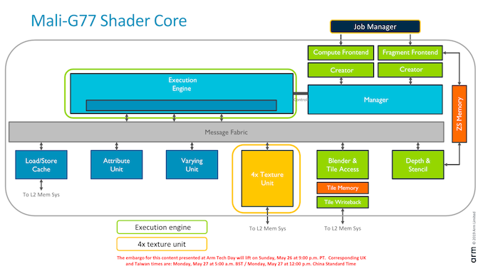
A shader core still contains the execution engine, load/store unit with cache, attribute unit, varying unit, texture mapping unit and pixel backend, as well as various other 3D fixed function blocks.
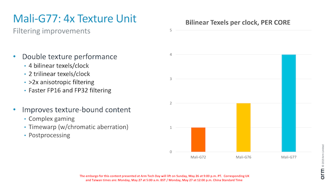
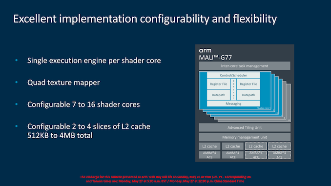
The biggest change here was on the texture unit block, which has doubled its throughput compared to the already doubled unit which we found on the Mali-G76.
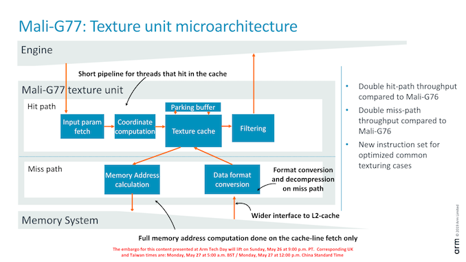
From a high-level functionality standpoint, the new TMU looks quite similar to its predecessor, however we find some very significant changes in terms of the throughput of the new design.
The design is prationioned into two “paths”, a hit- and miss-path that either deal with misses inside the cache or outside the texture cache. The hit-path is naturally a shorter more latency optimised path.
On the hit-path, the texture cache itself has been improved and is now 32KB and is able of 16 texels/cycle throughput. The filtering unit has also been improved and its throughput increased and now supports one quad per cycle for bilinear texturing, or half a quad per cycle for trilinear texturing, both 2x of G76’s throughput.
Interestingly, Arm says that the new TMU is roughly the same area as its predecessor yet still enabling this doubling of capability, which is quite a nice engineering feat.
Fundamentally this large increase in the texturing capability of a core changes the ALU:Tex ratio of the GPU. Even though ALU capability has increased by 33%, the doubling of the TMU throughput means that essentially we’re now back to a lower ratio, more in favour of texture throughput, whereas past GPUs focused on increasing the compute performance. Arm deemed this as a necessary change for workloads that are now starting to tax this aspect of GPUs more.
It’s to be noted that while the texture filtering throughput has increased, the actual pixel backend throughput has not. Here a shader core is still only able to draw out 2 pixels per clock, so we now have a 2:1 texel:pixel ratio whereas in the past it remained 1:1.
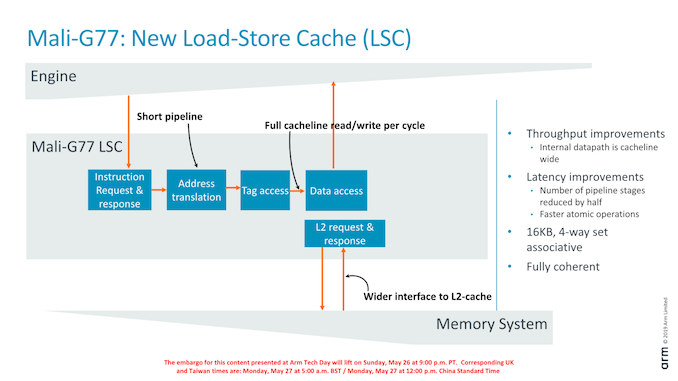
Another new redesign among the shader core blocks is a new load-store cache block. Functionally it’s the same as in the past, however it’s now been redesigned with more throughput in mind. Within the same area, the amount of pipeline stages have been reduced by half, further reducing the latency of the core’s operation. The bandwidth has been widened to a full cacheline width, which should be a doubling over its predecessor.
The actual cache is 16KB in size and 4-way set associative, and is said to be very useful for ML workloads.
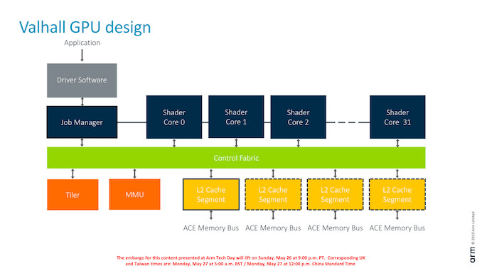
Putting all the pieces together and zooming out from a shader core to the GPU-level, we again see a large familiarity on how Arm organises its overall block. The architecture supports scaling shader cores from 1 core to 32 cores, although the microarchitecture of the G77 currently only supports up to 16 cores. Furthermore the current smallest design that Arm makes RTL ready for is a 7-core configuration, as the company deems customers going for smaller configurations would be better served by different IP (Such as the G52, or maybe a future unannounced IP in the same range).
The L2 cache still consists of up to four slices with each from 256KB to 1MB in size. Currently, most vendors have gone with 2MB configurations and I don’t think any licensee has ever implemented 4MB. In terms of bandwidth, the L2 to the LSC bandwidth has also doubled up from 32B/cycle to 64B/cycle (a full cacheline), while the external bandwidth depends on whether the vendor implements a 128-bit or 256-bit AXI interface to each of the L2 slices.
Performance Targets: 30% Better PPC and Efficiency
On paper, the new Valhall architecture and the new Mali-G77 certainly seem like big changes, but what will be more important is to see what the performance, efficiency, and area claims are.
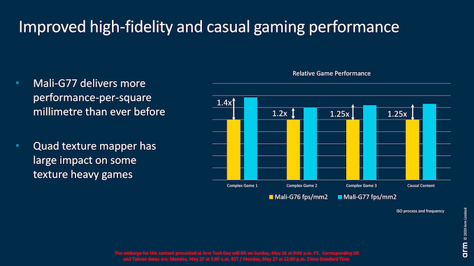
Arm’s performance claims are interesting because they’re being published in a performance per mm² basis. Due to how vendors implement their GPUs, in which they can vary core count as well as frequency, it’s hard to actually give a clear figure which describes the improvements between two discrete GPU configurations. In the case of the G77, Arm claims that the new IP is able to provide from 1.2x to 1.4x the performance/mm² compared to the G76. In absolute terms a G77 shader core is said to be about the same size as a G76 core.
What this means is that this could be directly translated into either a smaller GPU for the vendor, or simply more space to add in additional GPU cores and consequently increase the performance. Particularly Arm claims the G77 does very well in texture heavy games, so that will be something interesting to see in once devices actually come out and how different workloads will behave.
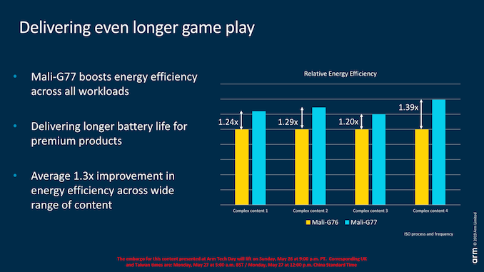
Another way to increase performance is to clock the GPU higher. Here the fundamental limit is the 4-5W TDP thermal envelope of smartphones. In a comparison at ISO-process and performance, the new G77 is said to use between 17% and 29% less energy and power to complete the same workloads. Or in other words, the performance/W is 1.2x to 1.39x better. Arm states that fundamentally frequency between the G76 and G77 shouldn’t change much at all, an internally Arm still targets and 850MHz sign-off.
This year I’m not going to attempt any performance and efficiency projections as there’s just too many variables at play. Among one of the larger changes for next year is that I’m expecting SoCs to support LPDDR5 which likely will change the power dynamics in smartphones by some notable margin.
Arm does note that they are expecting 1.4x performance jumps in next year’s SoCs with the G77. Using Samsung’s Exynos 9820 as the reference G76 implementation, this would mean that a future G77 SoC would come close with Apple’s A12 GPU’s performance at better power efficiency (assuming power levels are maintained). This would put Qualcomm in trouble as it would be a clear jump ahead of the current generation Adreno 640, however we expect Qualcomm to follow-up with a new generation GPU as well.
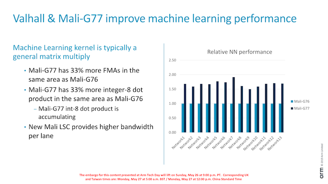
Machine learning performance of the G77 is something that Arm is quite proud of. Here it’s not just the fact that the cores have 33% more processing units, but also the much improved design of the LSC and its bandwidth that pushes inferencing performance of the G77 at an average of 1.6x the G76.
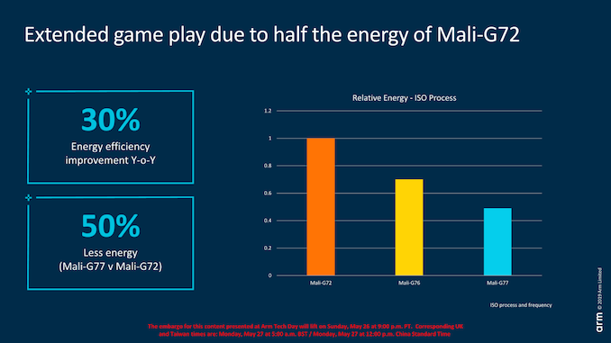
Finally, Arm made a generational comparison between the last two generation Mali GPUs. On the same process and at the same performance, the new G77 continues on track to 30% year-on-year energy efficiency improvements, and uses 50% less energy than a Mali-G72.
Conclusion & End Remarks
During the TechDay event Arm was clearly very excited about the new Valhall architecture and the new Mali-G77. There’s very much reason to be excited as it seems like Arm is about to showcase a significant generational jump in its Mali GPU IP.
The new G77 employs a brand-new architecture that fundamentally revamps Arm’s execution core, aiming for something more modern and in line with desktop GPU architectures. This seems like a shift that was long coming, as while the G76 was a relatively good GPU, the previous generation G72 and G71 weren’t.
I’m expecting to see the Mali-G77 in the next generation of Samsung Exynos and HiSilicon Kirin SoCs later this year and early next year. On paper and if everything goes right, the G77 should be able to close the performance and efficiency gap to Apple and Qualcomm. In particular the G77 should be able to leap ahead of Qualcomm’s Adreno GPUs, that is, at least against the current-generation.
I’m fairly optimistic, and now Arm as well as the partner licensees just need to execute properly for users to be able to enjoy the end-results.

