Original Link: https://www.anandtech.com/show/14384/arm-announces-cortexa77-cpu-ip
Arm's New Cortex-A77 CPU Micro-architecture: Evolving Performance
by Andrei Frumusanu on May 27, 2019 12:01 AM EST
2018 was an exciting year for Arm’s own CPU designs. Last year in May we saw the release of the Cortex-A76 and the subsequent resulting silicon in the form of the Kirin 980 as well as Snapdragon 855 SoCs. We were very impressed by the IP, and Arm managed to deliver on all its performance, efficiency and area promises, resulting in some excellent SoCs and devices powering most of 2019’s flagship devices.
This year we follow-up with another TechDay disclosure, and this time around we’re uncovering Arm’s follow-up to the Cortex-A76: the new Cortex-A77. The new generation is a direct evolution of last year’s major microarchitecture introduction, and represents the second instance of Arm’s brand-new Austin core family. Today we’ll analyse how Arm has pushed the IPC of its new microarchitecture and how this will translate into real performance for upcoming late-2019/early-2020 SoCs and devices.
Deimos turns to Cortex-A77
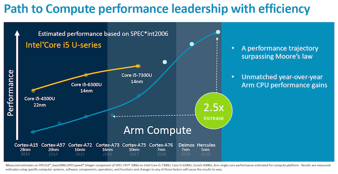
The announcement of the Cortex-A77 doesn’t come as a surprise as Arm continues on their traditional annual IP release cadence. In fact today is not the first time that Arm has talked about the A77: In August of last year Arm had teased the CPU core when releasing its performance roadmap through 2020:
Codenamed as “Deimos”, the new Cortex-A77 picks up where the Cortex-A76 left off and follows Arm’s projected trajectory of delivering a continued solid 20-25% CAGR of performance uplift with each generation of Arm’s new Austin family of CPUs.
Before we dwell into the new Cortex-A77, we should take a look back at how the performance of the A76 has evolved for Arm:
The A76 has certainly been a hugely successful core for Arm and its licensees. The combination of the brand-new microarchitecture alongside the major improvements that the 7nm TSMC process node has brought some of the biggest performance and efficiency jumps we’ve ever seen in the industry.
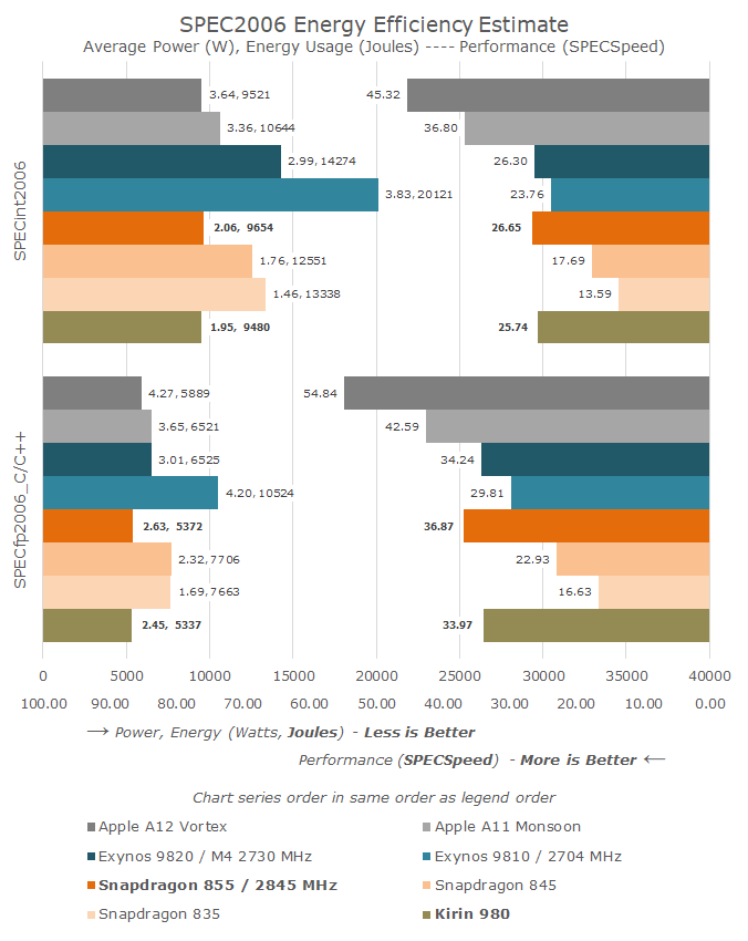
The results is that the Kirin 980 as well as the Snapdragon 855 both represented major jumps over their predecessors. Qualcomm has proclaimed a 45% leap in CPU performance compared to the previous generation Snapdragon 845 with Cortex-A75 cores, the biggest generational leap ever.
While the performance increase was notable, the energy efficiency gains we saw this generation was even more impressive and directly resulted in improved battery life of devices powered by the new Kirin and Snapdragon SoCS.
While the A76 performed well, we should remember that it does have competition. While Samsung’s own microarchitecture this year with the M4 has lessened the performance/efficiency gap, the Exynos CPU still largely lags behind by a generation, even though this difference is amplified by a process node difference this year (8nm vs 7nm). The real competition for Arm here lies with Apple’s CPU design teams: Currently the A11 and A12 still hold a large performance and efficiency lead that amounts to roughly two microarchitecture generations.
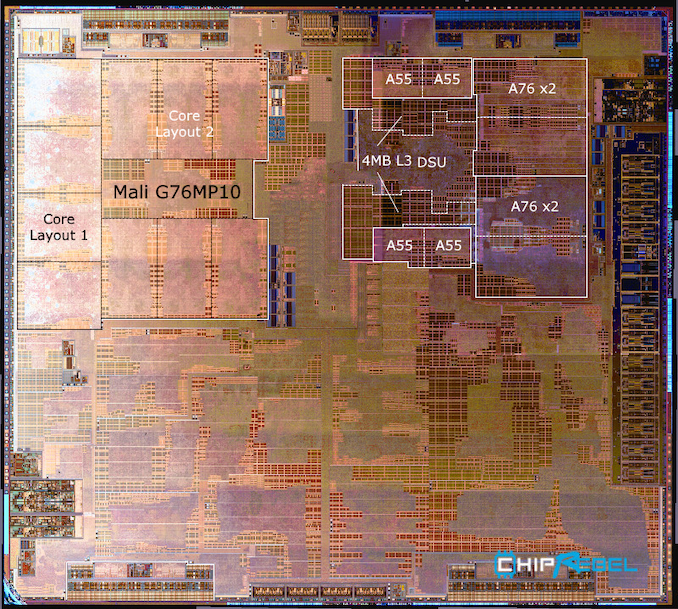
Die shot credit: ChipRebel - Block labelling: AnandTech
One of Arm’s fortes however remains in delivering the best PPA in the industry. Even though the A76’s performance didn’t quite match Apple’s, it managed to achieve outstanding efficiency with incredibly small die area sizes. In fact, this is a conscious design decision by Arm as power efficiency and area efficiency are among the top priorities for Arm’s licensees.
The Cortex-A77: A Top-Level Overview
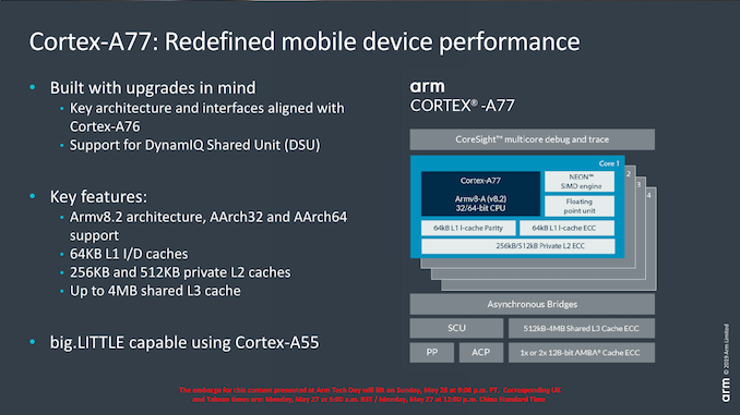
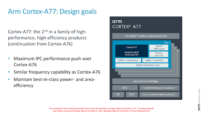
The Cortex-A77 being a direct microarchitectural successor to the A76 means the new core largely stays in line with the predecessor’s features. Arm states that the core was built in mind with vendors being able to simply upgrade the SoC IP without much effort.
In practice what this means is that the A77 is architecturally aligned with its predecessor, still being an ARMv8.2 CPU core that is meant to be paired with a Cortex-A55 little CPU inside of a DynamIQ Shared Unit (DSU) cluster.
Fundamental configuration features such as the cache sizes of the A77 also haven’t changed compared to its predecessor: We’re still seeing 64KB L1 instruction and data caches, along with a 256 or 512KB L2 cache. It’s interesting here that Arm did design the option for an 1MB L2 cache for the infrastructure Neoverse N1 CPU core (Which itself is derived from the A76 µarch), but chooses to stay with the smaller configuration options on the client (mobile) CPU IP.
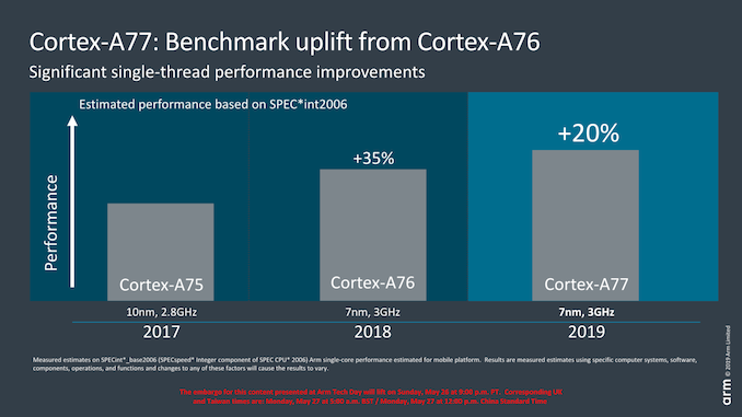
As an evolution of the A76, the A77 performance jump as expected won’t be quite as impressive, both from a microarchitecture perspective, but also from an absolute performance standpoint as we’re not expecting large process node improvements for the coming SoC generation.
Here the A77 is projected to still be productised on 7nm process nodes for most customers, and Arm is proclaiming a similar 3GHz peak target frequency as its predecessor. Naturally since frequency isn’t projected to change much, this means that the core’s targeted +20% performance boost can be solely attributed to the IP’s microarchitectural changes.
To achieve the IPC (Instructions per clock) gains, Arm has reworked the microarchitecture and introduced clever new features, generally beefing up the CPU IP to what results in a wider and more performant design.
The Cortex-A77 µarch: Going For A 6-Wide* Front-End
The Cortex-A76 represented a clean-sheet design in terms of its microarchitecture, with Arm implementing from scratch the knowledge and lessons of years of CPU design. This allowed the company to design a new core that was forward-thinking in terms of its microarchitecture. The A76 was meant to serve as the baseline for the next two designs from the Austin family, today’s new Cortex-A77 as well next year’s “Hercules” design.
The A77 pushes new features with the primary goals of increasing the IPC of the microarchitecture. Arm’s goals this generation is a continuation of focusing on delivering the best PPA in the industry, meaning the designers were aiming to increase the performance of the core while maintaining the excellent energy efficiency and area size characteristics of the A76 core.
In terms of frequency capability, the new core remains in the same frequency range as the A76, with Arm targeting 3GHz peak frequencies in optimal implementations.
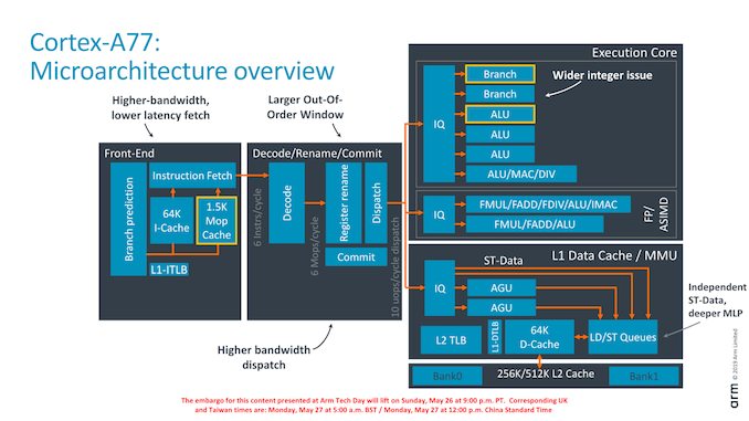
As an overview of the microarchitectural changes, Arm has touched almost every part of the core. Starting from the front-end we’re seeing a higher fetch bandwidth with a doubling of the branch predictor capability, a new macro-OP cache structure acting as an L0 instruction cache, a wider middle core with a 50% increase in decoder width, a new integer ALU pipeline and revamped load/store queues and issue capability.
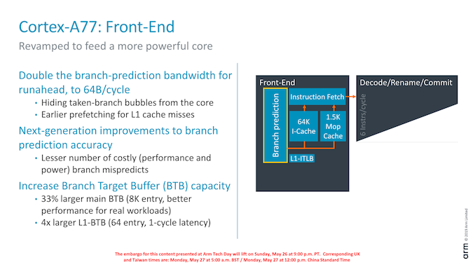
Dwelling deeper into the front-end, a major change in the branch predictor was that its runahead bandwidth has doubled from 32B/cycle to 64B/cycle. Reason for this increase was in general the wider and more capable front-end, and the branch predictor’s speed needed to be improved in order to keep up with feeding the middle-core sufficiently. Arm instructions are 32bits wide (16b for Thumb), so it means the branch predictor can fetch up to 16 instructions per cycle. This is a higher bandwidth (2.6x) than the decoder width in the middle core, and the reason for this imbalance is to allow the front-end to as quickly as possible catch up whenever there are branch bubbles in the core.
The branch predictor’s design has also changed, lowering branch mispredicts and increasing its accuracy. Although the A76 already had the a very large Branch Target Buffer capacity with 6K entries, Arm has increased this again by 33% to 8K entries with the new generation design. Seemingly Arm has dropped a BTB hierarchy: The A76 had a 16-entry nanoBTB and a 64-entry microBTB – on the A77 this looks to have been replaced by a 64-entry L1 BTB that is 1 cycle in latency.
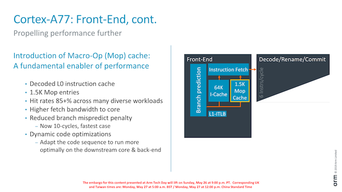
Another major feature of the new front-end is the introduction of a Macro-Op cache structure. For readers familiar with AMD and Intel’s x86 processor cores, this might sound familiar and akin to the µOP/MOP cache structures in those cores, and indeed one would be correct in assuming they have the similar functions.
In effect, the new Macro-OP cache serves as a L0 instruction cache, containing already decoded and fused instructions (macro-ops). In the A77’s case the structure is 1.5K entries big, which if one would assume macro-ops having a similar 32-bit density as Arm instructions, would equate to about 6KB.
The peculiarity of Arm’s implementation of the cache is that it’s deeply integrated with the middle-core. The cache is filled after the decode stage (in a decoupled manner) after instruction fusion and optimisations. In case of a cache-hit, then the front-end directly feeds from the macro-op cache into the rename stage of the middle-core, shaving off a cycle of the effective pipeline depth of the core. What this means is that the core’s branch mispredicts latency has been reduced from 11 cycles down to 10 cycles, even though it has the frequency capability of a 13 cycle design (+1 decode, +1 branch/fetch overlap, +1 dispatch/issue overlap). While we don’t have current direct new figures of newer cores, Arm’s figure here is outstandingly good as other cores have significantly worse mispredicts penalties (Samsung M3, Zen1, Skylake: ~16 cycles).
Arm’s rationale for going with a 1.5K entry cache size is that they were aiming for an 85% hit-rate across their test suite workloads. Having less capacity would take reduce the hit-rate more significantly, while going for a larger cache would have diminishing returns. Against a 64KB L1 cache the 1.5K MOP cache is about half the area in size.
What the MOP cache also allows is for a higher bandwidth to the middle-core. The structure is able to feed the rename stage with 64B/cycle – again significantly higher than the rename/dispatch capacity of the core, and again this imbalance with a more “fat” front-end bandwidth allows the core to hide to quickly hide branch bubbles and pipeline flushes.
Arm talked a bit about “dynamic code optimisations”: Here the core will rearrange operations to better suit the back-end execution pipelines. It’s to be noted that “dynamic” here doesn’t mean it’s actually programmable in what it does (Akin to Nvidia’s Denver code translations), the logic is fixed to the design of the core.
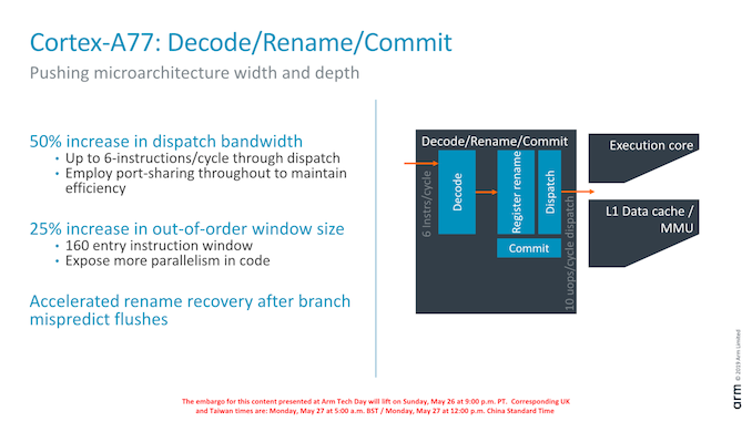
Finally getting to the middle-core, we see a big uplift in the bandwidth of the core. Arm has increased the decoder width from 4-wide to 6-wide.
Correction: The Cortex A77’s decoder remains at 4-wide. The increased middle-core width lies solely at the rename stage and afterwards; the core still fetches 6 instructions, however this bandwidth only happens in case of a MOP-cache hit which then bypasses the decode stage. In MOP-cache miss-cases, the limiting factor is still the decoder which remains at 4 instructions per cycle.
The increased width also warranted an increase of the reorder buffer of the core which has gone from 128 to 160 entries. It’s to be noted that such a change was already present in Qualcomm’s variant of the Cortex-A76 although we were never able to confirm the exact size employed. As Arm was still in charge of making the RTL changes, it wouldn’t surprise me if was the exact same 160 entry ROB.
The Cortex-A77 µarch: Added ALUs & Better Load/Stores
Having covered the front-end and middle-core, we move onto the back-end of the Cortex-A77 and investigate what kind of changes Arm has made to the execution units and data pipelines.
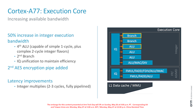
On the integer execution side of the core we’ve seen the addition of a second branch port, which goes along with the doubling of the branch-predictor bandwidth of the front-end.
We also see the addition on an additional integer ALU. This new unit goes half-way between a simple single-cycle ALU and the existing complex ALU pipeline: It naturally still has the ability of single-cycle ALU operations but also is able to support the more complex 2-cycle operations (Some shift combination instructions, logical instructions, move instructions, test/compare instructions). Arm says that the addition of this new pipeline saw a surprising amount of performance uplift: As the core gets wider, the back-end can become a bottleneck and this was a case of the execution units needing to grow along with the rest of the core.
A larger change in the execution core was the unification of the issue queues. Arm explains that this was done in order to maintain efficiency of the core with the added execution ports.
Finally, existing execution pipelines haven’t seen much changes. One latency improvement was the pipelining of the integer multiply unit on the complex ALU which allows it to achieve 2-3 cycle multiplications as opposed to 4.
Oddly enough, Arm didn’t make much mention of the floating-point / ASIMD pipelines for the Cortex-A77. Here it seems the A76’s “state-of-the-art” design was good enough for them to focus the efforts elsewhere on the core for this generation.
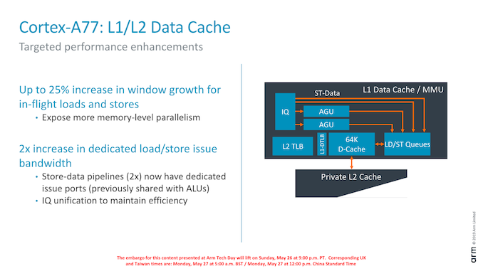
On the part of the load/store units, we still find two units, however Arm has added two additional dedicated store ports to the units, which in effect doubles the issue bandwidth. In effect this means the L/S units are 4-wide with 2 address generation µOps and 2 store data µOps.
The issue queues themselves again have been unified and Arm has increased the capacity by 25% in order to expose more memory-level parallelism.
Data prefetching is incredibly important in order to hide memory latency of a system: Shaving off cycles by avoiding to having to wait for data can be a big performance boost. I tried to cover the Cortex-A76’s new prefetchers and contrast it against other CPUs in the industry in our review of the Galaxy S10. What stood out for Arm is that the A76’s new prefetchers were outstandingly performant and were able to deal with some very complex patterns. In fact the A76 did far better than any other tested microarchitecture, which is quite a feat.
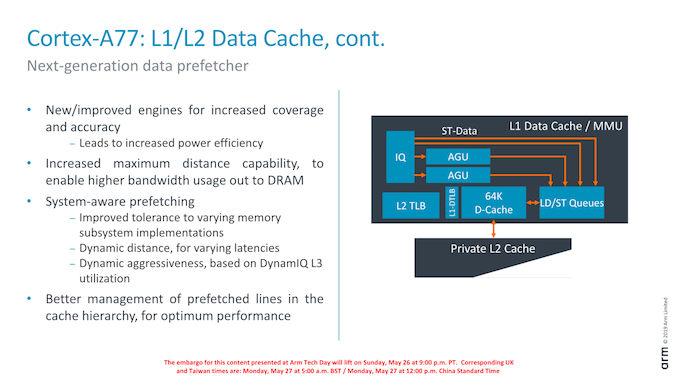
For the A77, Arm improved the prefetchers and added in even new additional prefetching engines to improve this even further. Arm is quite tight-lipped about the details here, but we’re promised increased pattern coverages and better prefetching accuracy. One such change is claimed to be “increased maximum distance”, which means the prefetchers will recognize repeated access patterns over larger virtual memory distances.
One new functional addition in the A77 is so called “system-aware prefetching”. Here Arm is trying to solve the issue of having to use a single IP in loads of different systems; some systems might have better or worse memory characteristics such as latency than others. In order to deal with this variance between memory subsystems, the new prefetchers will change the behaviour and aggressiveness based on how the current system is behaving.
A thought of mine would be that this could signify some interesting performance improvements under some DVFS conditions – where the prefetchers will alter their behaviour based on the current memory frequency.
Another aspect of this new system-awareness is more knowledge of the cache pressure of the DSU’s L3 cache. In case that other CPU cores would be highly active, the core’s prefetchers would see this and scale down its aggressiveness in order to possibly avoid thrashing the shared cache needlessly, increasing overall system performance.
Performance Targets: 20-35% Better IPC
The Cortex-A77 saw some interesting microarchitectural changes that promise to increase performance. The question now remains where exactly the targeted performance gains will end up at?
In terms of published performance improvements, Arm opted to stay with SPEC2006, 2017, GeekBench4 and LMBench memory bandwidth. Our focus here will be on SPEC2006 as it’s still the most relevant benchmark among the set for mobile.
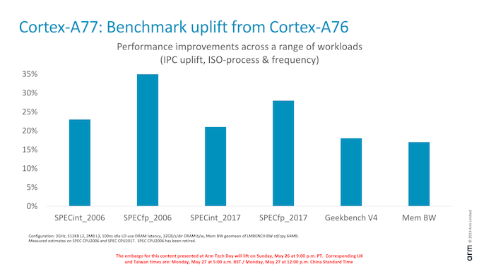
On SPECint2006, the A77 promises around a 23% IPC increase, while SPECfp2006 claims a more staggering 35% boost. The 23% increase for integer workloads was more or less in line with what we expected of the CPU core, however the 30-35% increase for FP workloads I must admit came as quite a surprise, particularly since we haven’t seen any significant changes on the FP execution units of the core. An explanation here would be that SPEC’s FP test suite is more memory intensive than the integer suite, and the Cortex-A77’s various microarchitectural improvements would be more visible in these workloads.
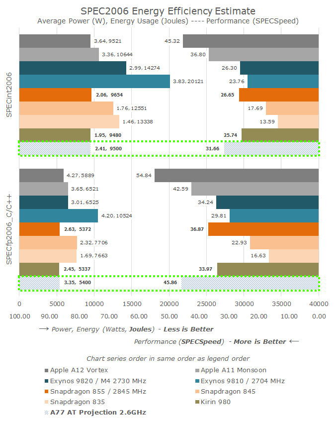
Last year I had made performance and efficiency projections for the A76 at two frequency points, and I ended up being quite close to where the Kirin 980 and Snapdragon 855 ended up landing. For the Cortex-A77, things should be a lot more straightforward to project as we won’t see major process node changes in the next generation 7nm SoCs.
Baselining on the current results of the Kirin 980, I simply extrapolated performance based on the published IPC increases for a theoretical 2.6GHz Cortex-A77 SoC. It’s to be noted that although Arm this year again talks about 3GHz target frequencies for the A77, I’m not expecting vendors to quite reach this frequency in upcoming SoCs, thus the 2.6GHz projection.
In terms of performance, the integer suite would see some solid improvement, however the floating-point results are a lot more interesting. If correct, the A77 would exceed the FP performance of Apple’s A11 and make for quite a big generational push even though we’re not expecting big process node improvements. It’s to be noted though that the A77 will have to compete with Apple’s A13 later this year as well as next-gen M5 cores from Samsung.
Arm promises energy efficiency of the A77 will remain the same as current-gen A76 SoCs. Thus at peak performance, both CPU cores would use the same amount of energy to complete a set workload. The increased performance of the A77 would however have one drawback: Increased power usage, linear with the increased performance figures. This latter increased power usage would seemingly reach levels where running more than two cores at peak frequency would be more problematic in a mobile SoC. Luckily, most vendors have moved on from 4 full-speed big cores to 2+2 or 3+1 designs where there’s only one or two high-power big cores.
It’s to be noted although we’re talking about big cores here, the A77 is said to be only 17% bigger than the A76 – still significantly smaller than the next best microarchitecture from the competition.
End Remarks
Overall the Cortex-A77 announcement today isn’t quite as big of a change as what we saw last year with the A76, nor is it as big a change as today’s new announcement of Arm’s new Valhall GPU architecture and G77 GPU IP.
However what Arm managed to achieve with the A77 is a continued execution of their roadmap, which is extremely important in the competitive landscape. The A76 delivered on all of Arm’s promises and ended up being an extremely performant core, all while remaining astonishingly efficient as well as having a clear density lead over the competition. In this regard, Arm’s major clients are still heavily focusing on having the best PPA in their products, and Arm delivers in this regard.
The one big surprise about the A77 is that its floating point performance boost of 30-35% is quite a lot higher than I had expected of the core, and in the mobile space, web-browsing is the killer-app that happens to be floating point heavy, so I’m looking forward how future SoCs with the A77 will be able to perform.
But even in the integer workloads a 20-25% IPC gain is absolutely marvellous improvement, and we do trust Arm to be able to maintain energy efficiency of the A76. Power will go up slightly, but I think the industry has shown that mobile devices today handle at least two higher power cores properly, so future SoCs should continue with big+middle+little CPU configurations.
Coming A77 SoCs from vendors are expected to still be 7nm – Qualcomm and HiSilicon are the two obvious leading customers that would adopt the core and I’m expecting similar timeframes as last generation’s chipsets. For now- Arm’s delivering on their promised 20-25% yearly CAGR and we believe this to continue for the foreseeable next few generations.

