Original Link: https://www.anandtech.com/show/1398
Socket 939 Roundup: Battle at the Top
by Wesley Fink on July 30, 2004 8:00 AM EST- Posted in
- Motherboards
Battle at the Top
The long-awaited Socket 939 Athlon 64 from AMD debuted on June 1 at Computex, but it has taken quite a while for Socket 939 motherboards to make their way into the retail channel. With the Socket 939 still perched at the top of the AMD product line, both in price and performance, the offerings still remain very small. We take a look at 6 new motherboards for Socket 939 from Abit, Asus, ECS, Gigabyte, and MSI.The Asus A8V Deluxe was not included in the original roundup because Asus told us a new Revision would soon be available. The Asus A8V Deluxe Revision 2.0, with a working AGP/PCI lock, was received a few days ago and has now been added to the roundup. We have included full test results from the Revison 2 A8V and compared it to the other 5 top-end 939 boards in the roundup. DFI has also announced a Socket 939 board based on the nForce3 Ultra chipset, but the retail introduction of that board is still several weeks away.
The Second-Generation chipsets for Athlon 64 represent a genuine improvement in features, flexibility, and performance for AMD's flagship processors. As you saw in our chipset review, the nForce3 has added the features to bring the nVidia chipsets to the competitive edge of Athlon 64 chipsets. The HyperTransport speed, which was widely criticized on the 150 chipset, is now 1000 in the Ultra version of the chipset used for 939. The chipset is, otherwise, the same as the 800 and 1000FSB versions that we saw in our Socket 754 Roundup: Comparing Generation 2. The on-chip Gigabit LAN and on-chip Firewall are unique and truly useful features among Athlon 64 solutions. nVidia also fixed the problems with their implementation of PCI/AGP lock on the 150, and we are finding a working PCI/AGP lock on every nForce3-250 motherboard that we test, just as nVidia promised.
VIA's update to their excellent K8T800 chipset was less dramatic as there are not many new features, but the improvements are just as dramatic under the hood. As you saw in our review of the K8T800 PRO chipset, VIA brings 1000 HyperTransport to the PRO chipset for all Athlon 64 Sockets - 940, 754, and 939. Perhaps the most significant improvement was the addition of a working PCI/AGP lock to the K8T800 PRO. Since all PRO chipsets support 1000 HT, the chipsets used in our Socket 754 Roundup: Comparing Generation 2 are the same as you will see in our 939 roundup.
As reported in the Socket 754 roundup and the Socket 939 launch review, VIA had early problems with their PCI/AGP lock. While we continued to see problems with a working AGP/PCI lock in early 939 samples, we are pleased to report that every vendor in our roundup now appears to have the VIA PCI/AGP lock working. If you have a VIA board with PCI/AGP lock issues, our advice is to contact your motherboard vendor for the latest BIOS or possibly a revised version of your motherboard. The good news is that VIA has worked with manufacturers to fix the issues, and the issues can be solved; the bad news is that there are still many VIA K8T800 PRO motherboards in the market with PCI/AGP lock issues, and some require a motherboard replacement to fix the problem. In some cases, we are looking at a third motherboard revision before we finally receive a working PCI/AGP lock on a VIA K8T800 PRO board.
Today, we are looking at 6 new Socket 939 motherboards, representing the top performance level for the Athlon 64, which is the fastest current CPU. Consider this roundup a search for the best of the best, since Socket 939 supports the top-performing Athlon 64 processors available in the fastest Dual-Channel memory configuration. The Gigabyte K8NSNXP-939 and MSI K8N Neo2 feature the nVidia nForce3 Ultra chipset, while the Abit AV8, Asus A8V Deluxe Rev. 2, ECS KV2 Extreme, and MSI K8T Neo2 are based on the VIA K8T800 PRO chipset.
Abit AV8: Features and Layout
| Abit AV8 Motherboard Specifications | |
| CPU Interface | Socket 939 Athlon 64 |
| Chipset | VIA K8T800 PRO/VT8237 |
| Bus Speeds | 200MHz to 336MHz (in 1MHz increments) |
| CPU Ratios | 4x - 25x in 1x increments |
| PCI/AGP Speeds | CPU:AGP:PCI - Fixed, 6:2:1, 7:2:1, 8:2:1 |
| HyperTransport | Auto, 200MHz to 1GHz (1x-5x) |
| Core Voltage | 1.50V to 1.85V in 0.025V increments |
| DRAM Voltage | 2.50V to 2.8V in 0.05V increments |
| AGP Voltage | 1.50V - 1.65V in 0.05V increments |
| NB (Northbridge) Voltage | 1.50V - 1.65V in 0.05V increments |
| SB (Southbridge) Voltage | 2.50V - 2.65V in 0.05V increments |
| HT (HyperTransport) Voltage | 1.20V - 1.40V in 0.05V increments |
| Memory Slots | Four 184-pin DDR DIMM Slots Dual-Channel Unbuffered Memory to 4GB |
| Expansion Slots | 1 AGP 8X Slot 5 PCI Slots |
| Onboard SATA/IDE RAID | 2 SATA 150 drives by VIA VT8237 Can be combined in RAID 0, 1, JBOD |
| Onboard IDE | Two Standard VIA ATA133/100/66 (4 drives) |
| Onboard USB 2.0/IEEE-1394 | 8 USB 2.0 ports supported by VIA VT8237 3 IEEE 1394 FireWire Ports |
| Onboard LAN | Gigabit Ethernet by VIA VT6122 PCI |
| Onboard Audio | Realtek ALC658 6-Channel with SPDIF |
| Tested BIOS | 1.3 |
The AV8 is Abit's flagship board for the Athlon 64, and you can certainly see this reflected in the features lavished on the AV8. Compared to the 754 version that we recently tested, Abit includes 3 Firewire ports on the AV8. True to their tradition as an overclocker's board, Abit has not included additional RAID, IDE or SATA controllers on the AV8. However, you will find that the VIA SATA RAID in the VT8237 Southbridge is fully supported. Abit has also used VIA chips for Firewire and LAN, but the VIA LAN is PCI-based and not on-chip as we see featured on the nVidia nF3-250 boards.
The overclocking controls are typically Abit in that they are a wonderful selection of voltages and frequencies to get the most from the K8T800 PRO and the Athlon 64. Particularly notable are the voltage adjustments for the Northbridge, Southbridge, and chipset - in addition to the expected voltage adjustments. The only surprise here is memory voltage, which is somewhat limited to 2.8V in BIOS. The latest version of uGuru (2.11) does not offer any additional vDIMM adjustments, so you are left with a top voltage of 2.8, which is limited for a board geared toward overclockers. We first tested uGuru in our review of the Abit KV8 Max3, and it continues to evolve as a very useful tool for the overclocker.
The first thing that we looked for was a working PCI/AGP lock, and we are pleased to report that the AV8 fully supports the AGP/PCI lock and a full range of ratios for overclocking the 939 processors. This is important because all Athlon 64 processors are unlocked downward, a side-effect of AMD Cool'n'Quiet technology. This means that any Athlon 64 can be set to lower CPU multipliers and higher frequencies to get the most out of high-speed memory. In addition, the Athlon 64 FX chips are completely unlocked, so both higher and lower ratios can be selected.
The Abit AV8 actually runs at 204 speed when the frequency is set to default, but we were able to force a 200 CPU frequency in BIOS for testing. All of the recent Abit boards that we have tested have been set to 204 at default, so be cautious in comparing review results unless the reviewer corrected the CPU frequency in testing an Abit motherboard.
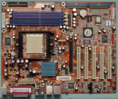
Abit uses flat edge connectors for IDE connections, which does a very good job of removing any interference from the bulky IDE cables. We like the edge connectors, but some case designs make it very difficult to connect the edge-connectors. The bulky 20-pin ATX and 4-pin 12V connectors are both between the CPU and the back panel I/O ports, which makes routing the 20-pin ATX without blocking air flow a challenge in most case designs. Abit included the 2-digit diagnostic LEDs, which can be very useful for troubleshooting.
Abit AV8: Overclocking and Stress Testing
FSB Overclocking Results
| Front Side Bus Overclocking Testbed | ||
| Processor: | Athlon 64 FX53 Socket 939 2.4GHz |
|
| CPU Voltage: | 1.5V (default) | |
| Cooling: | Thermaltake Silent Boost K8 | |
| Power Supply: | Antec TruePower 430W | |
| Maximum OC: (Standard Ratios) |
203 x13 2642MHz (+10.1%) |
|
| Maximum FSB: (Lower Ratio) |
280x9 (2520) at 1:1 Memory | |
Our FX53 easily achieved the next speed level of 2.6GHz on the Abit AV8. This will likely be the speed rating of the FX55, which will appear later this year. The best proof that the Abit has a working PCI/AGP lock can be seen in the fact that we were able to run DDR550 memory at 280x9 on the Abit. To achieve this overclock level, we needed to reduce the base HyperTransport frequency to 800. The AV8 could reach 300 CPU frequency at lower memory ratios and a 8 multiplier. We did find that the Abit did not really like an HT setting lower than 800, so we were limited to 300 as the maximum usable FSB.
Memory Stress Test Results:
The memory stress test measures the ability of the Abit AV8 to operate at its officially supported memory frequency (400MHz DDR), at the best performing memory timings that our Mushkin PC3500 Level 2 or OCZ PC3500 Platinum Ltd Modules will support. Memory stress testing was conducted by running RAM at 400MHz with 2 DIMM slots operating in Dual-Channel mode. The memory configuration of the Abit is a little unusual in that the first 2 DIMM slots represent a Dual-Channel. On most Dual-Channel motherboards, slots 1 and 3 are the first Dual Channel.| Stable DDR400 Timings - 2 DIMMs (2/4 DIMMs - 1 Dual-Channel Bank) |
|
| Clock Speed: | 200MHz |
| Timing Mode: | N/A |
| CAS Latency: | 2.0 |
| Bank Interleave: | N/A |
| RAS to CAS Delay: | 2T |
| RAS Precharge: | 10T* |
| Precharge Delay: | 2T |
| Command Rate: | 1T |
The Abit KV8 PRO was completely stable with 2 DIMMs in Dual-Channel at the best performing settings of 2-2-2-10, at 2.6V default voltage. It should be noted that the BH5 memory modules that we used for testing are no longer available for purchase, but we have not yet established our standard memory for future testing. We will be using a new standard memory in future motherboard tests.
As we first found in our latest Socket 754 roundup, the Command Rate is very important for top performance on a VIA chipset motherboard. The best performance is at a Command Rate of 1T, and the Abit AV8 was completely stable at a 1T setting with 2 DIMMs. Standard memory bandwidth measured with SiSoft Sandra 2004 SP2 shows a 6000 MB/s bandwidth with 1T Command Rate compared to a 5000 MB/s bandwidth with a 2T setting. While we could not set "Bank Interleave" in the BIOS, Sandra 2004 reported that a 2-way Bank Interleave was being used by the memory controller. With an on-CPU memory controller with Athlon 64, this is not as important a setting as it is on with chipset-based memory controllers.
Filling all four available memory slots is more strenuous on the memory subsystem than testing 2 DIMMs on a motherboard.
| Stable DDR400 Timings - 4 DIMMs (4/4 DIMMs - 2 Dual-Channel Banks) |
|
| Clock Speed: | 200MHz |
| Timing Mode: | N/A |
| CAS Latency: | 2.0 |
| Bank Interleave: | N/A |
| RAS to CAS Delay: | 2T |
| RAS Precharge: | 10T* |
| Precharge Delay: | 2T |
| Command Rate: | 2T |
The Abit AV8 was able to run with all 4 DIMM slots at the same aggressive 2-2-2-10 settings used for 2 DIMMs. However, Command Rate must be reduced to 2T when filling both Dual Channels.
During the course of testing for the 939 roundup, we experienced a failure of our FX53 processor. AMD was very gracious in quickly providing a replacement so testing could continue. The FX53 failure is probably rare, but the way that the CPU failed provided some insight into the Athlon 64 on-board memory controller. We first noticed new boards requiring much slower timings for memory; in most cases CAS 2.5 was required where CAS 2 had worked previously. This appeared to be motherboard differences, so we continued testing. Later, the FX53 failed. The replacement first went into a board where CAS 2.5 or 3 had been required, and now the same board performed fine at CAS 2 memory timings. Our point here is that the problem was the on-CPU memory controller failing and not the motherboard. The on-CPU memory controller is wonderful for reducing latency, but, unlike the past, memory problems may also be related to the CPU and not just the motherboard.
Asus A8V Deluxe: Features and Layout
| Asus A8V Deluxe - Revision 2.0 Motherboard Specifications |
|
| CPU Interface | Socket 939 Athlon 64 |
| Chipset | VIA K8T800 PRO/VT8237 |
| Bus Speeds | 200MHz to 300MHz (in 1MHz increments) |
| CPU Ratios | 4x - 20x in 0.5x increments |
| PCI/AGP Speeds | Auto, 66.66/33.33, 75.4/37.7 |
| HyperTransport | Auto, 200MHz to 1GHz (1x-5x) |
| Core Voltage | 0.80V to 1.80V in 0.025V increments |
| DRAM Voltage | Auto, 2.5V to 2.8V in 0.1V increments |
| AGP Voltage | 1.5V, 1.6V |
| V-Link Voltage | 2.5V, 2.6V |
| Memory Slots | Four 184-pin DDR DIMM Slots Dual-Channel Unbuffered Memory to 4GB |
| Expansion Slots | 1 AGP 8X Slot 5 PCI Slots |
| Onboard SATA/IDE RAID | 2 SATA 150 drives by VIA VT8237 Can be combined in RAID 0, 1, JBOD PLUS 2 SATA by Promise 20378 |
| Onboard IDE | Two Standard VIA ATA133/100/66 (4 drives) PLUS 1 IDE 133/100/66 by Promise 20378 |
| Onboard USB 2.0/IEEE-1394 | 8 USB 2.0 ports supported by VIA VT8237 2 IEEE 1394 FireWire Ports by VIA VT6307 |
| Onboard LAN | Gigabit Ethernet by Marvell 88E8001 |
| Onboard Audio | Realtek ALC850 8-Channel with SPDIF |
| Tested BIOS | 1006 Beta 2 |
When Asus first introduced the A8V Deluxe it was the only Socket 939 board we had received with no AGP/PCI lock. Asus did not advertise an AGP/PCI lock and, in fact, it was not even listed as an option. When we talked with Asus about why they would leave out such a key feature of the VIA K8T800 PRO chipset, we were told Asus had concerns about the stability of the feature, and would not release a board with a lock until they were confident of the stable operation of the feature. While we did receive several prototypes with impressive performance and a working lock, Asus US did not give us the go-ahead that these interim designs would ever become production boards. For that reason, we did not believe it was fair to AnandTech readers to review an excellent design that they might never see in production.

Several weeks ago, Asus advised that they had completed a new Revision 2.0 with a number of board refinements and a working PCI/AGP lock that would soon be released. We had been very pleased with the revisions of the A8V we had evaluated, so we had great expectations of Revision 2.0. As you will see in the performance numbers and overclocking of the Asus A8V we were not disappointed.
The A8V Deluxe is the top-of-the-line Asus board for Socket 939, as you see reflected in the feature set. The A8V can be considered an update of the successful Asus K8V with the significant addition of the VIA K8T800 PRO chipset with, finally, a working PCI/AGP lock. Asus tells us that Revision 2.0 is more than just the addition of a production PCI/AGP lock, as they also used the update as an opportunity to refine the design.
As the Asus flagship Socket 939 the A8V Deluxe provides all the expected VIA K8T800 PRO/VT8237 features like 2-drive SATA RAID, 8 USB ports, and Hyper Transport to 1GHz. In addition Asus adds Marvell Gigabit LAN, The Promise PDC20378 RAID controller supporting 2 more SATA drives plus an additional IDE connector, Firewire, and the Realtec ALC850 8-channel codec. Asus calls their top boards AI, and the A8V includes a long list of proprietary Asus AI features like C.P.R., AI Net, AI BIOS, EZ Flash BIOS, and Q-Fan 2 fan-speed controls. The A8V also fully supports AMD Cool'n'Quiet.
Too often, we forget to mention that Asus is a huge proponent of Wi-Fi, and most of their boards include Wi-Fi capabilities. The A8V Deluxe is another Wi-Fi Home board, but the included adapter is now the higher-speed Wi-Fi G instead of the older and slower B standard. Asus even includes a desktop antenna to ease your communication with a wireless router or to serve as host for other Wi-Fi computers.
The overclocking controls are excellent in their range as we have come to expect on Asus boards. Noteworthy are the ratios in fine 0.5x ratios which makes OC fine-tuning that much easier on 939 CPUs. The CPU voltage also covers a very wide range from 0.8V to 1.80 volts. Our only complaint here is that 300 CPU Clock is a little short for a board that can do 289 at 1:1 memory, and the memory voltage controls are really limited at a top of 2.8V when we have performance memory warranted to 3.0V. Otherwise the variety and range of BIOS adjustments is excellent.
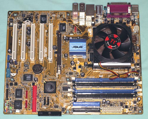
The layout of the A8V Deluxe is excellent. Both the 20-pin ATX and the 4-pin 12V connectors are on board edges and don't interfere with the CPU. The IDE connectors are in our preferred upper right edge of the board. Some will hate the floppy edge connector, but we liked getting it out of the way, and the floppy is also a connector many users don't use any way. The 4-dimm connectors, for up to 4GB of Dual-Channel memory, are well clear of the AGP 8X slot when changing memory. Asus is an advocate of quiet, failure-free passive chipset cooling, and you will see that in the massive heatsink used on the Northbridge. There's little to complain about in the layout of the Asus A8V Deluxe Rev.2.
Rear panel I/O is also very complete, including 6 audio mini jacks, both optical and coaxial SPDIF outputs, 4 USB, LAN, Firewire, 1 serial port, parallel port, and the usual PS2 keyboard and mouse ports. We were particularly pleased to see easily accessible optical and coax SPDIF ports and wish other manufacturers paid as much attention to this feature as Asus has in their recent board designs.
Asus A8V Deluxe: Overclocking and Stress Testing
FSB Overclocking Results
| Front Side Bus Overclocking Testbed | ||
| Processor: | Athlon 64 FX53 Socket 939 2.4GHz |
|
| CPU Voltage: | 1.5V (default) | |
| Cooling: | Thermaltake Silent Boost K8 | |
| Power Supply: | Antec TruePower 430W | |
| Maximum OC: (Standard Ratios) |
204 x 13 2652MHz (+10.5%) |
|
| Maximum FSB: (Lower Ratio) |
289x9 (2601) at 1:1 Memory | |
The A8V Deluxe Revision 2 has come a long way from the first revision that didn't even have an AGP/PCI lock. Revision 2 is in a virtual dead heat with our top-performing MSI K8N Neo2 at 289 x9 with our Shikatronics DDR550 memory. The A8V also matched the highest OC with this FX53 at 204x13 at default voltage. This overclocking performance is as good as we are accustomed to seeing on the best nForce3 Ultra boards, and can only be called superb when achieved with the VIA K8T800 PRO, which is not always the best overclocker. To achieve this overclock level, we needed to reduce the base Hyper Transport frequency to 800.
Memory Stress Test Results:
The memory stress test measures the ability of the the Asus A8V Deluxe to operate at its officially supported memory frequency (400MHz DDR) at the best performing memory timings our Mushkin PC3500 Level 2 or OCZ PC3500 Platinum Ltd Modules will support. Memory stress testing was conducted by running RAM at 400MHz with 2 DIMM slots operating in Dual-Channel mode. The memory configuration of the Asus is the more standard setup with slots 1 and 3 are the first Dual Channel.| Stable DDR400 Timings - 2 DIMMs (2/4 DIMMs - 1 Dual-Channel Bank) |
|
| Clock Speed: | 200MHz |
| Timing Mode: | N/A |
| CAS Latency: | 2.0 |
| Bank Interleave: | Enabled |
| RAS to CAS Delay: | 3T |
| RAS Precharge: | 10T* |
| Precharge Delay: | 2T |
| Command Rate: | 1T |
The Asus K8V Deluxe Rev.2 was completely stable with 2 dimms in Dual-Channel at the settings of 2-2-3-10 at 2.6V default voltage with 1T command rate. This is very slightly slower than the timings than worked on other Socket 939 boards. While we could run the majority of benchmarks at 2-2-2 timings, there were a few that were not completely stable until we increased Ras-to-Cas delay to 3. It should be noted that the BH5 memory modules we used for testing are no longer available for purchase, but we have not yet established our standard memory for future testing. We will be using a new standard memory in future motherboard tests.
As we first found in our latest Socket 754 roundup, the Command Rate is very important for top performance on a VIA chipset motherboard. The best performance is at a Command Rate of 1T, and the Asus A8V was completely stable at a 1T setting with 2 dimms. We set 'Bank Interleave' to 'Enabled' in the BIOS, and Sandra 2004 SP2 reported a 2-way Bank Interleave was being used by the memory controller. With an on-CPU memory controller with Athlon 64, this is not as important a setting as it is on with chipset-based memory controllers.
Filling all four available memory slots is more strenuous on the memory subsystem than testing 2 DIMMs on a motherboard.
| Stable DDR400 Timings - 4 DIMMs (4/4 DIMMs - 2 Dual-Channel Banks) |
|
| Clock Speed: | 200MHz |
| Timing Mode: | N/A |
| CAS Latency: | 2.0 |
| Bank Interleave: | Enabled |
| RAS to CAS Delay: | 2T |
| RAS Precharge: | 10T* |
| Precharge Delay: | 2T |
| Command Rate: | 2T |
We see a very interesting result with all 4 dimm banks filled. The Asus A8V was able to run with all 4 dimm slots at more aggressive 2-2-2-10 settings than the 2-2-3-10 required for 2 dimms. Please keep in mind, though, that the Command Rate must be reduced to 2T when filling both Dual Channels, and the memory is actually a bit slower even though the other timings are slightly faster. The A8V Deluxe is also very picky about the settings that are used with 4 dimms in the 'Enable 2T' option in BIOS. If an Auto setting is used with 4 dimms the board tries to set 1T and single channel memory at a lower memory speed. If 'Auto' is selected and memory timings are forced to DDR400 the board would not boot. With 4 dimms, you will need to set the 2T option to 'Enable 2T' for proper Dual-Channel operation at DDR400.
ECS KV2 Extreme: Features and Layout
| ECS KV2 Extreme Motherboard Specifications | |
| CPU Interface | Socket 939 Athlon 64 |
| Chipset | VIA K8T800 PRO/VT8237 |
| Bus Speeds | 200MHz to 511MHz (in 1MHz increments) |
| CPU Ratios | 4x - 20x in 0.5x increments |
| PCI/AGP Speeds | Disabled, 66.0, 75.4 |
| HyperTransport | 1GHz to 200MHz (5x-1x) |
| Core Voltage | 0.825V to 1.55V in .025V increments |
| DRAM Voltage | 2.50V to 2.7V in 0.05V increments |
| AGP Voltage | 1.45V, 1.53V, 1.57V, 1.60V |
| Chipset Voltage | None |
| Memory Slots | Four 184-pin DDR DIMM Slots Dual-Channel Unbuffered Memory to 4GB |
| Expansion Slots | 1 AGP 8X Slot 5 PCI Slots |
| Onboard SATA/RAID | 2 SATA 150 drives by VIA VT8237 plus 2 SATA 150 by SiS 180 Can be combined in RAID 0, 1, 0+1, JBOD |
| Onboard IDE | Two Standard VIA ATA133/100/66 (4 drives) plus 2 IDE 133/100/66 by SiS 180 |
| Onboard USB 2.0/IEEE-1394 | 8 USB 2.0 ports supported by VIA VT8237 2 IEEE 1394a FireWire Ports by VIA VT6307 |
| DUAL Onboard LAN | Gigabit Ethernet by Marvel 88E8001 plus 10/100 by VIA VT6103L |
| Onboard Audio | Realtek ALC655 6-Channel with SPDIF |
| Tested BIOS | 1.1A |
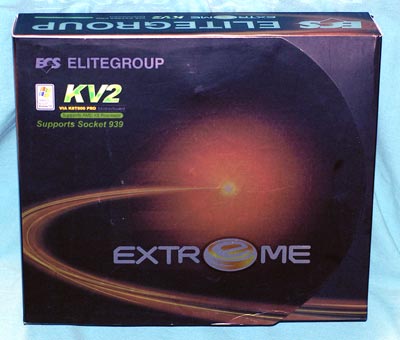
ECS hopes that the bronze-foil box with a feature flap clearly announces that the ECS KV2 Extreme is a premium board. The Extreme name is reserved for the top ECS boards, and with the Socket 939 currently a premium board, the KV2 announces that ECS wants to be a contender at the top.
The KV2 Extreme even has the individual interior boxes that we first saw on Abit motherboards, carefully fitted to protect the manuals and brackets . This should not come as a complete surprise, since ECS also manufactures some motherboards for Abit. The KV2 is a 6-layer, 3-phase design, which includes all the bells and whistles that you have come to expect from top-of-the-line motherboards. This includes Dual RAID, Dual LAN, 4 SATA ports, 2 Firewire ports, provisions for 6 IDE drives, and active North Bridge cooling.
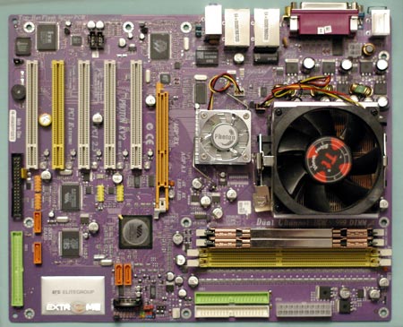
Just so you don't miss it, ECS even has a silver plaque on the purple KV2 announcing it is a member of the Extreme series. The layout of the board is generally excellent, showing great attention to the smallest details. ECS has placed the ATX, IDE, and floppy connectors in our preferred upper right edge location. Even the extra IDE for the 5th and 6th IDE is out of the way for the PCI slots.
The BIOS adjustments on the early versions of the KV2 were very sparse, but ECS quickly updated the KV2 Extreme with the CPU Frequency adjustments, ratios, and PCI/AGP lock that you would expect on a premium 939 motherboard. Our only complaints about the available options are that the vCore is still rather meager with a top of 1.55V; 1.70 volts would have been preferred. Also, the vDIMM to only 2.7V is low for a board that intends to compete in this arena - a range to at least 2.85V and preferably 3.0V would be better.
The range of CPU Frequency adjustments to 511 is incredible, but we found that we could only use a very small portion of that frequency range. While we verified that the AGP/PCI lock is working with a PCI Geiger, we were still limited in our overclocking attempts compared to other VIA boards in this roundup.
ECS KV2 Extreme: Overclocking and Stress Testing
FSB Overclocking Results
| Front Side Bus Overclocking Testbed | ||
| Processor: | Athlon 64 FX53 Socket 939 2.4GHz |
|
| CPU Voltage: | 1.5V (default) | |
| Cooling: | Thermaltake Silent Boost K8 | |
| Power Supply: | Antec TruePower 430W | |
| Maximum OC: (Standard Ratios) |
207FSB x 12.5 2587MHz (+8%) |
|
| Maximum FSB: (Lower Ratio) |
220FSB x 11 at 1:1 Memory | |
Our FX53 topped out at about 2.59 GHz on the ECS KV2, which is slightly below the 2.6+ achieved on the top 939 boards. However, ECS has the significant advantage of half multipliers, which are very useful for tweaking the KV2 for the best performance with any Athlon 64 CPU. While we clearly found a working PCI/AGP lock with PCI Geiger, the ECS still topped out at 219-220 CPU frequency in BIOS - a figure you would expect on a good board without a lock.
We were able to reach higher in Windows with the ECS overclocking utility, which they call Fuzzy OC, reaching a high of 236 at a multiplier of 10. We have seen this type of behavior on other early VIA K8T800 PRO boards, and we suspect ECS will be able to significantly improve these results with a BIOS update or board revision. If ECS manages to deliver better overclocking performance, the KV2 Extreme will be a formidable competitor. For now, we can say it performs quite well at stock speeds, and offers great promise in the overclocking area. It just isn't quite there yet as an enthusiast board.
Memory Stress Test Results:
The memory stress test basically determines the ability of the ECS KV2 to operate at its officially supported memory frequency (400MHz DDR), at the best performing memory timings that our Mushkin PC3500 Level 2 or OCZ PC3500 Platinum Ltd Modules will support. Memory stress testing was conducted by running RAM at 400MHz with 2 DIMM slots operating in Dual-Channel mode. ECS uses the more standard DC configuration of slots 1 and 3 for the first Dual-Channel bank, and 2 and 4 for bank 2.| Stable DDR400 Timings - 2 DIMMs (2/4 DIMMs - 1 Dual-Channel Bank) |
|
| Clock Speed: | 200MHz |
| Timing Mode: | N/A |
| CAS Latency: | 2.0 |
| Bank Interleave: | N/A |
| RAS to CAS Delay: | 2T |
| RAS Precharge: | 10T* |
| Precharge Delay: | 2T |
| Command Rate: | 1T |
The premium design of the KV2 paid off in memory performance, as the ECS was completely stable with 2 DIMMs in Dual-Channel at the best performing settings of 2-2-2-10. We have found that the best performance on Socket 939 boards is with a Command Rate of 1T, and the KV2 was very stable with a 1T Command Rate setting.
Filling all four available memory slots is more strenuous on the memory subsystem than testing 2 DIMMs on a motherboard.
| Stable DDR400 Timings - 4 DIMMs (4/4 DIMMs - 2 Dual-Channel Banks) |
|
| Clock Speed: | 200MHz |
| Timing Mode: | N/A |
| CAS Latency: | 2.0 |
| Bank Interleave: | N/A |
| RAS to CAS Delay: | 2T |
| RAS Precharge: | 10T* |
| Precharge Delay: | 2T |
| Command Rate: | 2T |
The ECS was able to run with all 4 DIMM slots at the same aggressive 2-2-2-10 settings used for 2 DIMMs. However, as we have seen on other 939 boards running all 4 DIMMs, Command Rate must be reduced to 2T when filling both Dual Channels.
Gigabyte K8NSNXP-939: Features and Layout
| Gigabyte K8NSNXP-939 Motherboard Specifications | |
| CPU Interface | Socket 939 Athlon 64 |
| Chipset | nVidia nForce3 Ultra |
| Bus Speeds | 200MHz to 455MHz (in 1MHz increments) |
| CPU Ratios | 5x to 25x in 0.5x increments |
| PCI/AGP Speeds | Auto, 66MHz to 100MHz (in 1MHz increments) |
| HyperTransport | 1x-5x (200MHz to 1GHz) |
| Core Voltage | 0.8V to 1.70V in 0.025V increments |
| DRAM Voltage | +.1V, +.2V |
| AGP Voltage | +.1V, +.2V, +.3V |
| HyperTransport Voltage | +.1V, +.2V, +.3V |
| Memory Slots | Four 184-pin DDR DIMM Slots Dual-Channel Unbuffered Memory to 4GB |
| Expansion Slots | 1 AGP 8X Slot 5 PCI Slots |
| Onboard SATA/RAID | nVidia 2-Drive SATA(RAID 0, 1) Plus SiI3512 2-Drive SATA (RAID 0, 1) |
| Onboard IDE/RAID | Two Standard nVidia ATA133/100/66 (4 drives). Can be combined with SATA drives for RAID 0, 1, 0+1, JBOD |
| Onboard USB 2.0/IEEE-1394 | 8 USB 2.0 ports supported by nF3-250 2 1394B FireWire ports by TI controller |
| Dual Onboard LAN | 1Gigabit Ethernet by Marvell 8001 10/100 Ethernet by ICS 1883 |
| Onboard Audio | Realtek ALC850 8-Channel with UAJ |
| Tested BIOS | M03 Beta |
More than any other manufacturer, Gigabyte loads their premium boards with every feature that you can think of, and then some. The K8NSNXP-939 certainly follows in that tradition as a member of the 6-Dual Deluxe family. Gigabyte has also developed a reputation of providing some of the widest ranges of adjustments to allow the Computer Enthusiast to squeeze the last bit of performance from their board, CPU, and memory, and the 939 continues that tradition.
The one glaring area that continues to plague recent Gigabyte designs is the extremely limited range of memory voltage adjustments. In this case, memory can be adjusted to +.2V and that's it. After seeing this complaint voiced in review after review, you would think that Gigabyte would seriously consider a wider range of vDIMM adjustments. Offsetting the limited vDIMM is a decent range of CPU voltage adjustments and the excellent addition of HyperTransport voltage options.
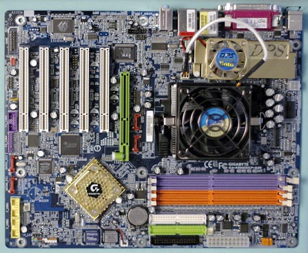
The most notable features of the K8NSNXP-939 include high-speed 1394B Firewire for firewire fanciers, Dual LAN, extensive RAID capabilities spanning SATA and IDE drives, and 8-channel audio with UAJ. We were also impressed with the updated design of the DPS 6-phase power module. It now sits lower on the board and our past complaints that the DPS impeded air flow are now history in the new design.
Layout of the Gigabyte 939 is nearly ideal, with the added step that even the SATA connectors are in locations that will not interfere with the largest PCI and AGP cards. The unique AGP EZ-Fix slot is also proving to be very useful, especially when using top-line 2-slot video cards. Anyone who has tried to remove a 6800 Ultra from a common rear-lever AGP slot probably cursed the designer and maybe broke the lever trying to find it under 2 slots of video card in a sea of capacitors. That's not to say EZ-Fix is that easy with a 2-slot card, but at least you have a fighting chance of removing the card. Gigabyte also kept capacitors away from the AGP slot.
Gigabyte K8NSNXP-939: Overclocking and Stress Testing
FSB Overclocking Results
| Front Side Bus Overclocking Testbed | ||
| Processor: | Athlon 64 FX53 Socket 939 2.4GHz |
|
| CPU Voltage: | 1.5V (default) | |
| Cooling: | Thermaltake Silent Boost K8 | |
| Power Supply: | Antec TruePower 430W | |
| Maximum OC: (Standard Ratios) |
204FSB x13 2652MHz (+10.5%) |
|
| Maximum FSB: (Lower Ratio) |
267FSB x 9 at 1:1 Memory | |
Our FX53 easily achieved the next speed level of 2.6GHz on the Gigabyte. In fact, the two nVidia nF3 boards tied for the highest overclock of this FX53 at 2652MHz. This is a bit faster than the 2.6GHz, which will likely be the speed rating of the FX55 to appear later this year. On recent Gigabyte boards, the BIOS overclocks have been more modest, with the rest of the overclock only doable with EZTune in Windows. It is good to see Gigabyte allowing a higher OC in BIOS, since we could achieve 267 in BIOS at lower multipliers. However, any higher value requires EZTune after booting into the OS. We still did not reach spectacular levels with EZTune, topping out about 280, but these levels should be more than enough to satisfy most users.
Memory Stress Test Results:
Since you need a score card for Dual Channel setup on 939, DIMMs 1 and 2 are the first DC bank on the Gigabyte, and yes, this can be very confusing. Our advice is to check memory and your start-up screen carefully to make sure that you are really in Dual-Channel mode when setting up a 939. Everyone seems to be doing it differently.The memory stress test is very basic, as it simply tests the ability of the Gigabyte K8NSNXP-939 to operate at its officially supported memory frequency (400MHz DDR), at the best performing memory timings that our Mushkin PC3500 Level 2 or OCZ PC3500 Platinum Ltd Modules will support. Memory stress testing was conducted by running RAM at 400MHz with 2 DIMM slots in a Dual-Channel configuration.
| Stable DDR400 Timings - 2 DIMMs (2/4 DIMMs - 1 Dual-Channel Bank) |
|
| Clock Speed: | 200MHz |
| Timing Mode: | N/A |
| CAS Latency: | 2.0 |
| Bank Interleave: | N/A |
| RAS to CAS Delay: | 2T |
| RAS Precharge: | 10T* |
| Precharge Delay: | 2T |
| Command Rate: | 1T |
The Gigabyte 939 was completely stable with two DIMMs in Dual-Channel mode at the best 1T Command Rate settings.
Filling all four available memory slots is more strenuous on the memory subsystem than testing 2 DIMMs on a motherboard.
| Stable DDR400 Timings - 4 DIMMs (4/4 DIMMs - 2 Dual-Channel Banks) |
|
| Clock Speed: | 200MHz |
| Timing Mode: | N/A |
| CAS Latency: | 2.0 |
| Bank Interleave: | N/A |
| RAS to CAS Delay: | 2T |
| RAS Precharge: | 10T* |
| Precharge Delay: | 2T |
| Command Rate: | 2T |
The K8NSNXP-939 was able to run with all 4 DIMM slots at the same aggressive 2-2-2-10 settings used for 2 DIMMs. However, as we have seen on the other 939 boards running all 4 DIMMs, Command Rate must be reduced to 2T when filling both Dual Channels.
MSI K8N Neo2 Platinum: Features and Layout
| MSI K8N Neo2 Platinum Motherboard Specifications | |
| CPU Interface | Socket 939 Athlon 64 |
| Chipset | nVidia nForce3 Ultra |
| Bus Speeds | 200MHz to 300MHz (in 1MHz increments) |
| CPU Ratios | 4x to 20x in 1x increments |
| PCI/AGP Speeds | Auto, 66MHz to 100MHz (in 1MHz increments) |
| HyperTransport | 1x-5x (200MHz to 1GHz) |
| Core Voltage | CPU default to 1.85V in .05V increments |
| DRAM Voltage | Auto, 2.55V to 2.85V in .05V increments |
| AGP Voltage | Auto, 1.55V to 1.85V in.05V increments |
| Dynamic Overclocking | 1%, 3%, 5%, 7%, 9%, 11% |
| Memory Slots | Four 184-pin DDR DIMM Slots Dual-Channel Unbuffered Memory to 4GB |
| Expansion Slots | 1 AGP 8X Slot 5 PCI Slots |
| Onboard SATA/RAID | 4 SATA 150 drives by nf3-250 Ultra Can be combined in RAID 0, 1, 0+1, JBOD |
| Onboard IDE/RAID | Two Standard VIA ATA133/100/66 (4 drives) Can be combined with SATA drives for RAID 0, 1, 0+1, JBOD |
| Onboard USB 2.0/IEEE-1394 | 8 USB 2.0 ports supported by nF3-250 3 IEEE 1394A FireWire Ports |
| Onboard LAN | Gigabit Ethernet by nForce3-250 Ultra |
| Onboard Audio | Realtek ALC850 8-Channel with SPDIF |
| Tested BIOS | 1.0B34 |
The MSI K8N Neo2 was the Reference Motherboard for the nVidia launch of the 939 chipset. We were very impressed with the performance of the Reference Board, and in fact, recommended the K8N Neo2 as the 939 motherboard of choice in our last High-End Buyers Guide. Several days ago, we finally received the K8N Neo2 retail board, so we were very anxious to verify what we had already found and perform additional testing on the K8N Neo2. We think that you will find the results in our comparative tests very interesting.
The K8N Neo2 combines all the features that you would expect on a top 939 motherboard, including the on-chip nVidia Gigabit LAN, nVidia on-chip Firewall, 4 SATA ports and 4 IDE ports that can be combined in nVRAID, 8 USB 2 ports, 8-channel audio, and 3 1394A firewire ports. MSI has implemented every nVidia nForce3-250 feature, so for more information on those features, you may want to review nForce3-250 - Part 1: Taking Athlon 64 to the Next Level and nForce3-250 - Part 2: Taking Athlon 64 to the Next Level.
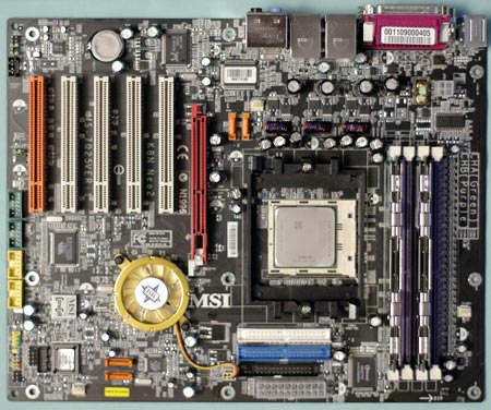
While the layout of the K8N Neo2 is a bit unusual, it works very well in most case designs. The 4 DIMM slots are on the top edge of the board, leaving the space around the CPU and AGP slot much clearer. The IDE and floppy connectors are all well clear of the CPU and PCI slots, and the 20-pin ATX and 4-pin 12V power connectors are on board edges that won't have to cross the top of the CPU fan. All of the IEEE, USB, audio, and front panel jumpers are below the slots at the bottom of the board - so even they are clear of the PCI slot area.
The voltage and overclocking options on the K8N Neo2 are generally very good, but we quickly reached the 300 CPU frequency limit of the board. MSI really needs to provide a wider available range of frequency settings, since this is one board that can use the additional settings. While 2.85V is a decent range for memory voltage, we would also prefer to see a range to 3.0V or even higher for those push memory to the limits. Half-multipliers also allow finer tweaking and would be a welcome addition to a future K8N BIOS.
With a board that does so many things so well you always wish for a little bit more, but that does not take away from the excellent performance of the K8N Neo2.
MSI K8N Neo2 Platinum: Overclocking and Stress Testing
FSB Overclocking Results
| Front Side Bus Overclocking Testbed | ||
| Processor: | Athlon 64 FX53 Socket 939 2.4GHz |
|
| CPU Voltage: | 1.5V (default) | |
| Cooling: | Thermaltake Silent Boost K8 | |
| Power Supply: | Antec TruePower 430W | |
| Maximum OC: (Standard Ratios) |
204FSBx13 2652MHz (+10.5%) |
|
| Maximum FSB: (Lower Ratio) |
290FSB x 9 (2610) at 1:1 Memory (+10%) | |
The K8N Neo2 allowed our DDR550 memory to reach the highest 1:1 performance that we have tested on any motherboard - P4 or A64. 290 Frequency (1160 FSB/HT) was the limit of our memory and the K8N reached it rather easily. By reducing the memory ratio a bit, we were right at the board limit of 300, and we could likely reach even higher OC levels with a wider range of frequency choices. The MSI K8N Neo2 was clearly the best overclocker of this roundup.
Memory Stress Test Results:
The memory stress test simply checks the ability of the K8N Neo2 to operate at its officially supported memory frequency (400MHz DDR), at the best performing memory timings that our Mushkin PC3500 Level 2 or OCZ PC3500 Platinum Ltd Modules will support. Memory stress testing was conducted by running RAM at 400MHz with 2 DIMM slots filled.| Stable DDR400 Timings - 2 DIMMs (2/4 DIMMs - 1 Dual-Channel Bank) |
|
| Clock Speed: | 200MHz |
| Timing Mode: | N/A |
| CAS Latency: | 2.0 |
| Bank Interleave: | N/A |
| RAS to CAS Delay: | 2T |
| RAS Precharge: | 10T* |
| Precharge Delay: | 2T |
| Command Rate: | 1T |
Like the other 939 motherboards in this roundup, the K8N Neo2 was completely stable with 2 DIMMs at the best performing settings of 2-2-2-10 at default speed and 2.6V default voltage. While a full memory comparison of the nVidia and VIA chipsets is beyond the scope of this roundup, we did run several SiSoft Sandra 2004 SP2 runs of the memory test module. At default settings, and the aggressive 2-2-2-10 timings on the FX53, the nF3-250 Ultra showed memory bandwidth in the 6100 range for FPU and Float. The same test on the VIA K8T800 PRO boards showed memory bandwidth in the 6000 range. Performance of both chipsets at the 1T setting was very similar. 2T Command Rates, with everything else the same, generated bandwidths of 4900 to 5000Mb/second.
Filling all four available memory slots is more strenuous on the memory subsystem than testing 2 DIMMs on a motherboard.
| Stable DDR400 Timings - 4 DIMMs (4/4 DIMMs - 2 Dual-Channel Banks) |
|
| Clock Speed: | 200MHz |
| Timing Mode: | N/A |
| CAS Latency: | 2.0 |
| Bank Interleave: | N/A |
| RAS to CAS Delay: | 2T |
| RAS Precharge: | 10T* |
| Precharge Delay: | 2T |
| Command Rate: | 2T |
The MSI K8N Neo2 was able to run with all 4 DIMM slots at the same aggressive 2-2-2-10 settings used for 2 DIMMs. However, as we have seen on the other 939 boards running all 4 DIMMs, Command Rate must be reduced to 2T when filling both Dual Channels.
MSI K8T Neo2-FIR: Features and Layout
| MSI K8T Neo2-FIR Motherboard Specifications | |
| CPU Interface | Socket 939 Athlon 64 |
| Chipset | VIA K8T800 PRO/VT8237 |
| Bus Speeds | 200MHz to 280MHz (in 1MHz increments) |
| CPU Ratios | 4 - 20x in 1x increments |
| PCI/AGP Speeds | Default, 66, 76.4 |
| HyperTransport | 1x-5x (200MHz to 1GHz) |
| Core Voltage | CPU default to 1.85V in .05V increments |
| DRAM Voltage | Auto, 2.55V to 2.85V in .05V increments |
| AGP Voltage | Auto, 1.55V to 1.85V in.05V increments |
| HT Voltage | Auto, 1.26V, 1.32V, 1.38V |
| Dynamic Overclocking | 3.3%,5%, 6.6%, 8%, 10%, 11%, 15% |
| Memory Slots | Four 184-pin DDR DIMM Slots Dual-Channel Unbuffered Memory to 4GB |
| Expansion Slots | 1 AGP 8X Slot 5 PCI Slots |
| Onboard SATA/IDE RAID | 2 SATA 150 drives by VIA VT8237 Can be combined in RAID 0,1,JBOD plus 2 SATA 150 Promise 20579 |
| Onboard IDE | Two Standard VIA ATA133/100/66 (4 drives) PLUS 2 IDE by Promise 20579 |
| Onboard USB 2.0/IEEE-1394 | 8 USB 2.0 ports supported by VT8237 3 IEEE 1394 FireWire Ports by VIA 6306 |
| Onboard LAN | Gigabit Ethernet by Realtek 8110S |
| Onboard Audio | Realtek ALC850 8-Channel with SPDIF |
| Tested BIOS | 1.0 |
MSI seems to have had a lock on supplying Reference Boards for the Socket 939 launch. While the K8N Neo2 was the Reference board for the nVidia 939 launch, a special version of MSI K8T Neo2 was the Reference Board for the AMD Socket 939 launch. You can find more information on both MSI boards in our Socket 939 Chipset Launch article.
The K8T Neo2 retail board adds many adjustments and tweaking options to the basic K8T Neo2 that we reviewed at launch. MSI also supplied a board with a working PCI/AGP lock just prior to the completion of this roundup, but it took several boards to finally get there. We have been assured that shipping K8T Neo2 boards will have working PCI/AGP locks and we are passing this information to you. When we finally received a fully working board, the K8T Neo2 was a decent performer and certainly one of the best of the VIA K8T800 PRO chipset Socket 939 boards.
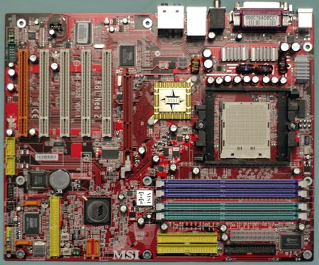
The K8T Neo2 is available in several versions with different options depending on price. Our test board was the top-line version, which added a Promise 20579 SATA/IDE RAID controller and VIA IEEE 1394A Firewire. Layout of the board is more conventional than the MSI K8N Neo2, with the 4 DIMM slots to the upper right, and the IDE/floppy and ATX connectors on the upper right. The 4-pin 12V connector is difficult to route as it sits almost in the center of the board. The additional IDE and SATA connections are all in areas that could potentially interfere with longer PCI cards, but the AGP 8X is clear of obstruction for a large top-end video card.
MSI K8T Neo2-FIR: Overclocking and Stress Testing
FSB Overclocking Results
| Front Side Bus Overclocking Testbed | ||
| Processor: | Athlon 64 FX53 Socket 939 2.4GHz |
|
| CPU Voltage: | 1.5V (default) | |
| Cooling: | Thermaltake Silent Boost K8 | |
| Power Supply: | Antec TruePower 430W | |
| Maximum OC: (Standard Ratios) |
200FSB x12 2600MHz (+10%) |
|
| Maximum FSB: (Lower Ratio) |
263FSB x 9 at 1:1 Memory | |
While the K8T Neo2 reached the next performance level of 2.6GHz at a 13 multiplier, it was not the CPU frequency overclocker that we see in the nVidia-based K8N Neo2. No matter the multiplier, the top frequency that we could reach with stability was 263, much lower than the 290 on the K8N Neo2, or the 280 reached on the Abit AV8.
Memory Stress Test Results:
The memory stress test is very basic, and simply tests the ability of the K8T Neo2 to operate at its officially supported memory frequency (400MHz DDR), at the best performing memory timings that our Mushkin PC3500 Level 2 or OCZ PC3500 Platinum Ltd Modules will support. Memory stress testing was conducted by running RAM at 400MHz with 2 DIMM slots in a Dual-Channel configuration with a Command Rate setting of 1T.| Stable DDR400 Timings - 2 DIMMs (2/4 DIMMs - 1 Dual-Channel Bank) |
|
| Clock Speed: | 200MHz |
| Timing Mode: | N/A |
| CAS Latency: | 2.0 |
| Bank Interleave: | N/A |
| RAS to CAS Delay: | 2T |
| RAS Precharge: | 10T (10T for Best Performance)* |
| Precharge Delay: | 2T |
| Command Rate: | 1T |
The K8T Neo2 had no problem at all with 2 dimms at aggressive 2-2-2-10 timings and a 1T Command Rate. We were frankly surprised at how well all the boards handled our BH5 memory, since it has sometimes been a problem memory on Athlon 64 boards. We do have to wonder if this is really the memory, however, or just the truly excellent memory controller on our replacement FX53.
Filling all four available memory slots is more strenuous on the memory subsystem than testing 2 DIMMs on a motherboard. We really expected to have to make concessions to memory timing with 4 DIMMs on all the 939 motherboards, but in fact, every board in the roundup had no problem with 2-2-2-10 timings at 1T.
| Stable DDR400 Timings - 4 DIMMs (4/4 DIMMs - 2 Dual-Channel Banks) |
|
| Clock Speed: | 200MHz |
| Timing Mode: | N/A |
| CAS Latency: | 2.0 |
| Bank Interleave: | N/A |
| RAS to CAS Delay: | 2T |
| RAS Precharge: | 10T* |
| Precharge Delay: | 2T |
| Command Rate: | 2T |
The MSI K8T Neo2 was able to run with all 4 DIMM slots at the same aggressive 2-2-2-10 settings used for 2 DIMMs. As we have seen on the other 939 boards running all 4 DIMMs, the Command Rate must be reduced to 2T when filling both Dual Channels.
Performance Test Configuration
If you are interested in more information comparing the Athlon 64, Athlon 64 FX, Prescott, P4, and P4EE, please see our in-depth comparisons in the recent 775/939/Prescott/3400+/3000+ launch reviews:Intel's 925X & LGA-775: Are Prescott 3.6 and PCI Express Graphics any Faster?
Intel 925X/915: Chipset Performance & DDR2
Socket 939 Chipsets: Motherboard Performance & PCI/AGP Locks
AMD Athlon 64 3800+ and FX-53: The First 939 CPUs
The Athlon 64 FX-53: AMD's Next Enthusiast Part
Intel's Pentium 4 E: Prescott Arrives with Luggage
Athlon64 3400+: Part 2
AMD's Athlon 64 3400+: Death of the FX-51
Athlon64 3000+: 64-bit at Half the Price
| Performance Test Configuration | |
| Processor(s): | AMD Athlon64 FX53 (2.4GHz) Socket 939 |
| RAM: | 2 x 512MB Mushkin PC3500 Level II OR 2 x 512MB OCZ PC3500 Platinum Ltd |
| Hard Drive(s): | Seagate 120GB 7200 RPM IDE (8MB Buffer) |
| Video AGP & IDE Bus Master Drivers: | NVIDIA nForce Platform Driver 4.24 (5-10-2004) VIA 4in1 Hyperion 4.51 (12-02-2003) |
| Video Card(s): | nVidia 6800 Ultra (AGP 8X) |
| Video Drivers: | nVidia nForce 61.80 Beta |
| Operating System(s): | Windows XP Professional SP1 |
| Motherboards: | Abit AV8 PRO (VIA K8T800 PRO) Asus A8V Deluxe Revision 2 (VIA K8T800 PRO) ECS KV2 Extreme (VIA K8T800 PRO) Gigabyte K8NSNXP-939 (nVidia nForce3 Ultra) MSI K8N Neo2 Platinum (nVidia nForce3 Ultra) MSI K8T Neo2-FIR (VIA K8T800 PRO) |
Tests used either Mushkin PC3500 Level II or OCZ PC3500 Platinum Ltd memory modules. Both memories use Winbond BH5 chips and perform virtually the same in our benchmarks. The BH5 memory modules that we used for testing are no longer available for purchase, but we have not yet established our standard memory for future testing. We will be using a new standard memory in future motherboard tests.
Since the nVidia 6800 Ultra PCI Express card was used for testing in the 925X/915 chipset launch, we used the AGP 8X version of the 6800 Ultra for all testing in this roundup. This allows for better comparison with Intel Socket 775 results, since our standard ATI 9800 PRO is not available in a PCIe configuration. We are still evaluating video cards to determine our new Video standard for future benchmarking. All performance tests were run with AGP Aperture set to 128MB with Fast Write enabled. Resolution in all benchmarks is 1024x768x32 unless otherwise noted.
Additions to Performance Tests
AutoGK (Auto Gordian Knot) has been selected as the new standard for Encoding benchmarking. This benchmark is partially based on the DVD2AVI engine and we use DivX 5.1.1 as the encoding codec. Test results are compiled with a 2-pass encoding using "Sum of All Fears", Chapter 9 as the video source.Game Benchmarks
We have added four new Gaming tests to our standard suite of gaming benchmarks. Far Cry is a popular DirectX 9.0b game, which is run with a custom benchmark called Airstrip. We have also added Unreal Tournament 2004 with a custom benchmark called UTBench. Return to Castle Wolfenstein - Enemy Territory is a recent OpenGL game based on the Quake engine, and we run the Radar benchmark. We are finding RCW-ET to be an excellent benchmark for measuring system performance, and it will likely replace Quake3 as our standard OpenGL benchmark down the road. We have also included the Final Fantasy XI benchmark, which is DX9. With the addition of the 4 new games, we have dropped Splinter Cell from our motherboard game benchmarks.Other standard game benchmarks include Halo, Microsoft's Direct X 9.0b game; X2 Benchmark, a DX 8.1 game, which includes Transform and Lighting effects; the DX9 Aquamark 3; and Unreal Tournament 2003, which is included for comparison with the new UT2004 test results. The DX 8.1 Comanche 4 benchmark is also used with the 4X anti-aliasing setting a 1280x1024 resolution to differentiate system performance better using the nVidia 6800 Ultra.
General Performance and Encoding
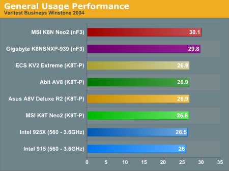
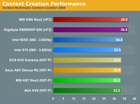
We never expected the nVidia nForce3 Ultra to be a better performer in Winstone benchmarks than the VIA K8T800 PRO. However, both the nF3 Ultra boards are outperforming the VIA boards by a significant percentage. Since the nVidia 6800 Ultra video card was used for all benchmarking in the roundup, we plan to verify these results with an ATI X800 XT as soon as that board is available to the Motherboard Lab for testing.
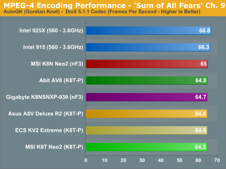
The performance of the Socket 939 boards in the new AuotGK 2-pass Media Encoding benchmark was also a mild surprise. We expected Intel to retain their lead in media encoding due to our logical choice of DivX 5.1.1 as the encoding codec. This codec fully exploits some of the features of the Intel chipset, like SSE3, and generally favors the Intel processors. The DVD2AVI engine at the heart of AutoGK, on the other hand, generally favors AMD processors. It appears that you can really show whatever you wish in encoding these days depending on the Encoding program and codec used. Anand did extensive research on media encoding and chose the new AutoGK/DivX 5.1.1. as our new standard due to the fair, balanced and respected results obtained with this combination.
It certainly looks like the combination of Socket 939, FX53, and AutoGK/DivX 5.1.1 balances the field for media encoding. The difference between top systems from AMD and Intel is now less than 3% with Divx, which can be considered equivalent. A quick check using a 2-pass test with the Xvid codec shows the Intel 3.6 at 35.2 and the AMD FX53 at 35.8, again essentially a dead heat. The upcoming move to 64-bit encoding should significantly boost Athlon 64 performance, giving A64 a formidable lead in encoding benchmarks.
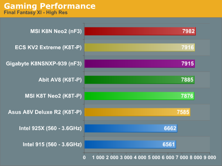
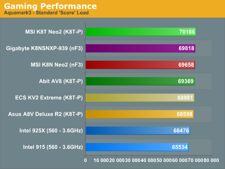
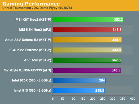
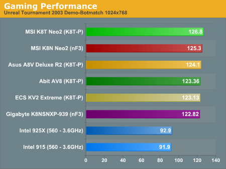
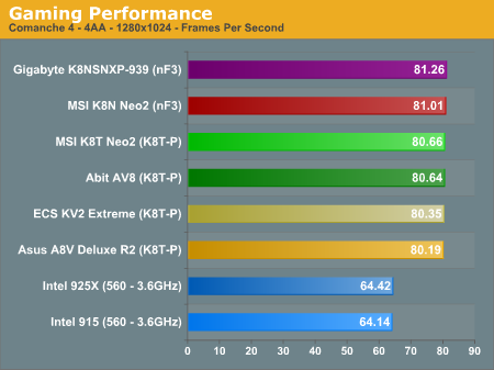
DirectX 9 Gaming Performance
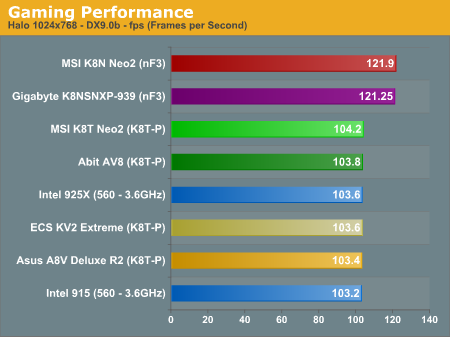
Intel's Socket 775 has not really changed anything in Gaming Performance. The Athlon 64 FX53 on a Socket 939 board still completely dominates gaming across the board. The general performance of the VIA and nVidia-based 939 boards was virtually the same in DirectX 9 games, with one notable exception. Microsoft's Halo performs almost 15% better on the nVidia nForce3 Ultra. We have no explanation for these performance differences with these chipsets in Halo, but we do plan to investigate this further when we can repeat the tests with an ATI X800 XT video card.
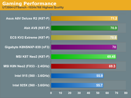
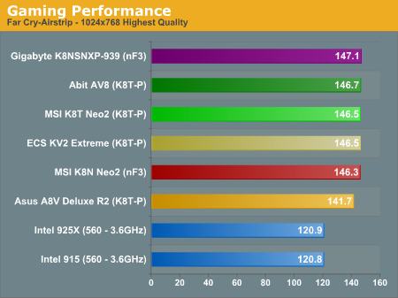
DirectX 8 & OpenGL Gaming Performance
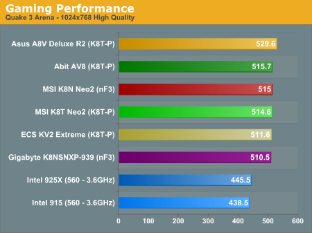
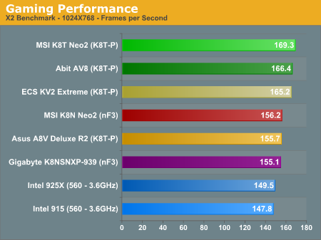
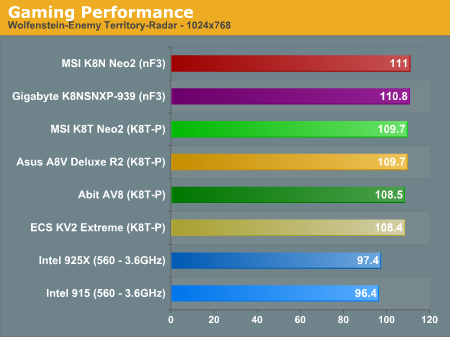
DX8 and OpenGL games show the same consistent performance between the VIA and nVidia 939 chipsets except for X2 and RCW-ET. X2, a Direct X 8.1 game with demanding T&L (transform and lighting effects), performs best on a VIA chipset, while Wolfenstein-Enemy Territory, an OpenGL game, is best on nForce3. We do plan to take a closer look at Halo, X2, and RCW-ET performance when we can repeat the tests with an ATI X800 XT video card.
Generally, the domination of the Socket 939 results compared to Intel's top Pentium 4 560 (3.6GHz) on the top 925X chipset is not a pretty picture for Intel, in DX9, DX8, or OpenGL. Clearly, the Athlon 64 processors in general, and the Socket 939 in particular, continue their domination of Gaming benchmarks.
Workstation Performance
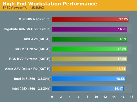
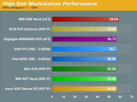
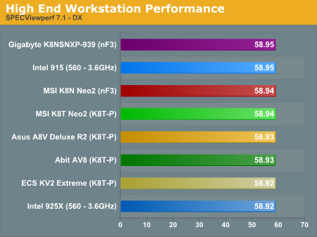
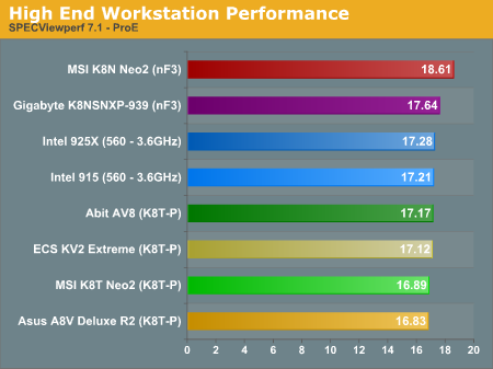
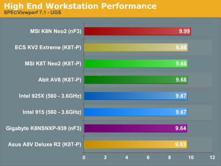
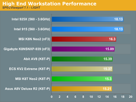
On the whole. we see a pattern of even workstation performance between the top Intel 560 on 775 and the top AMD FX53 on 939. The only exceptions are Intel topping Light as it usually does, and the FX53 topping 3dsMax. The nForce and VIA chipset boards were fairly even in SPECviewperf except for the standout performance of the K8N Neo2. Otherwise, there is little separating the performance of any of these boards in Workstation Performance.
Final Words
It was difficult to resist being a little sensationalist in this 939 roundup and titling the review, "Who needs 925X?" That would have been a fair title, however, since you can clearly see that all of the Socket 939/FX53 boards completely outperform Intel's top 560 on the top 925X motherboard. Even Media Encoding, the last bastion of Intel dominance, is now a dead heat with the new AutoGK benchmark.Any of the Socket 939 motherboards that we tested here would make a great home for a Socket 939 Athlon 64. They all perform very well at stock speed and any of them will serve you well. We even found that all six of the tested motherboards performed at the fastest timings available and a 2T Command Rate with 4 DIMMs on board, so even that is a non-issue.
However, in this go-round, there are a few criteria that begin to separate the boards that we tested. The two nForce3 Ultra motherboards did particularly well in Winstones, outperforming the VIA K8T800 PRO boards in these important benchmarks of overall real-world performance. We also found that the two nF3 boards in this roundup were consistent top performers, and, like other nF3-250 boards that we have tested, are complete with a working PCI/AGP lock for overclocking. This is not a criticism of VIA, because every VIA-based board that we tested in this roundup does indeed have a working lock. However, our concern remains that it sometimes took 2 or 3 revisions to get that working lock on the VIA boards - an issue that we have yet to see on any of the nForce3-250 boards. The good news is we are now confident that VIA has the PCI/AGP lock working, but there are boards floating around without this working feature. Our advice is to be cautious in a VIA purchase if this is an important specification for you. A little time for the market to settle should remove any concerns that you might have in buying a VIA K8T800 PRO chipset 939 or 754.
The KV2 Extreme is a remarkable step forward for ECS, and we can heartily recommend it as a good value if you plan to run only at stock speeds or you will only need modest overclocking capabilities. It is a very good effort at producing an Enthusiast-level ECS board. However, we think that this board needs to mature a bit more before it turns into a board that will satisfy most enthusiasts. We feel similarly about the MSI K8T Neo2-FIR, which was somewhat a surprise as the socket 754 K8T Neo was a favorite. Our concern is based on the fact that we went through 3 K8T Neo2 boards before we got one that really worked. That may just be coincidence, but it raises concern about the quality assurance of this particular product. The final board works very well, and is very fast at stock speed, but it falls well short of the remarkable overclocking capabilities of the sister K8N Neo2. A little time will likely take care of this issue, but we remain cautious for the time being.
Of our top four boards, we can honestly say that any of these 4 would be a great choice. The K8N Neo2 and Gigabyte K8NSNXP are both based on the nForce3 Ultra chipset, and the Abit AV8 and Asus A8V Deluxe Revision 2 are very clearly the top of the VIA boards, reaching our second best overclocks at 289 and 280. However, if you look carefully at the features, performance results, and just plain class in a market segment filled with top performers, the MSI K8N Neo2 stands out.
 |
Based on top performance, the full implementation of the nForce3 Ultra features, value, overclocking performance, and flexibility, the MSI K8N Neo2 Platinum emerges from a class of top Socket 939 Athlon 64 boards as our Gold Editors Choice. This makes the K8N Neo2 our choice as the best Athlon 64 motherboard that you can buy. MSI has produced two excellent motherboards in a row based on nVidia chipsets for Athlon 64. The K8N Neo for A64 Socket 754 was also one of our top choices for Single-Channel Athlon 64. The K8N Neo2 continues that performance as the top Athlon 64 motherboard that you can buy. |
The choice for Silver Editor's Choice is a bit more difficult. We could make arguments for the nF3 Ultra Gigabyte K8NSNXP-939, the VIA K8T800 PRO Abit AV8, or the VIA Asus A8V Deluse Rev. 2. However, when we look closely at value, we find the Abit and Asus are both much cheaper to buy than the Gigabyte, which sways our choice in those directions. As a result the Silver Editors Choice is a tie between two VIA K8T800 PRO motherboards - the Abit AV8 and the Asus A8V Deluxe Revision 2. Please note the award to Asus ONLY applies to Revision 2, since the first revision does not have a reliable working PCI/AGP lock.
 |
We are extremely pleased to award the Silver Editors Choice for best Athlon 64 Socket 939 motherboard to the Abit AV8. Abit proved you can build an excellent Enthusiast 939 motherboard, and have all the overclocking bells and whistles, with the VIA chipset. The Abit was not a standout in any one area in our tests, but it is a very balanced motherboard with all the Enthusiast features that we have come to expect from Abit motherboards. It is also an excellent value among Socket 939 motherboards. Abit has worked very hard to reach this level of performance with the VIA chipset, and they have produced a board that is really fun to use. |
|
It gives great pleasure to also award the AnandTech Silver Editors Choice to the Asus A8V Deluxe Revision 2. It took Asus quite a while to get to this point, but there is a lot to like, and little to dislike, with the A8V Deluxe Revision 2. The A8V is not generally the fastest board here, this distinction now belongs to the nF3 Ultra boards, but it is definitely one of the best overclockers in the entire roundup. Asus has finally delivered on the promise of that first A8V, which reached high but just could not quite make the cut. Revision 2 is all we hoped we would see, and Asus deserves congratulations for the perseverance to stay the course and finally deliver one of the best Socket 939 boards on the market. While we still lean toward the nVidia nForce3 Ultra as the better solution for round 2 of the Athlon 64 chipset wars, there is no doubt Asus has massaged the K8T800 PRO for all it's worth - delivering the kinds of headroom we didn't think would even be possible with the VIA chipset. We can only admire the kind of Engineering prowess that took the A8V to what we see today. |
There are no real losers in this roundup, but there are clearly some winners that stand above the crowd. We look forward to the evolution of the 939 as the mainstream Athlon 64 socket, because that will bring even more choices to the marketplace. For now, there are several outstanding homes for your new 939 CPU, but in the future there will be even more choices, and even more opportunites for a new winner to emerge. That's what makes this industry fun for some and maddening for others - there is always the possibility something better is just around the corner.


