Original Link: https://www.anandtech.com/show/13959/arm-announces-neoverse-n1-platform
Arm Announces Neoverse N1 & E1 Platforms & CPUs: Enabling A Huge Jump In Infrastructure Performance
by Andrei Frumusanu on February 20, 2019 9:00 AM EST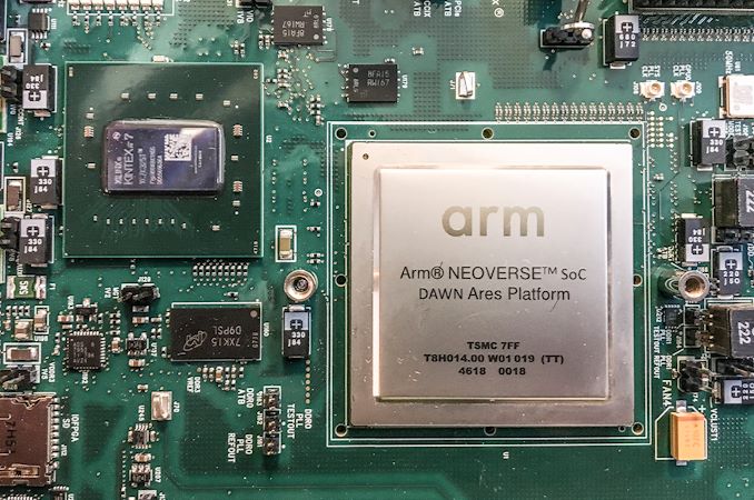
Anybody following the industry over the last decade will have heard of Arm. We best know the company for being the enabler and providing the architecture as well as CPU designs that power essentially all of today’s mobile devices. The last 7-5 years in particular we’ve seen meteoric advances in silicon performance of the mobile SoCs found in our smartphones and tablets.
However Arm's ambition goes widely beyond just mobile and embedded devices. The market for compute in general is a lot larger than that, and looking at things in a business sense, high-end devices like servers and related infrastructure carry far greater profit margins. So for a successful CPU designer like Arm who is still on the rise, it's a very lucrative market to aim for, as current leader Intel can profess.
To that end, while Arm has been wildly successful in mobile and embedded, anything requiring more performance has to date been out of reach or has come with significant drawbacks. Over the last decade we’ve heard of numerous prophecies how products based on the architecture will take the server and infrastructure market by storm “any moment now”. In the last couple of years in particular we’ve seen various vendors attempt to bring this goal to fruition: Unfortunately, the results of the first generation of products were less than successful, and as such, even though some did better than others, the Arm server ecosystem has seen a quite a bit of hardship in its first years.
A New Focus On Performance
While Arm has been successful in mobile for quite some time, the overall performance of their designs has often left something to be desired. As a result, the company has been undertaking a new focus on performance that is spanning everything from mobile to servers. Working towards this goal, 2018 was an important year for Arm as the company had introduced its brand-new Cortex A76 microarchitecture design: Representing a clean-sheet endeavor, learning from the experience gained in previous generations, the company has put high hopes in the brand-new Austin-family of microarchitectures. In fact, Arm is so confident on its upcoming designs that the company has publicly shared its client compute CPU roadmap through 2020 and proclaiming it will take Intel head on in PC laptop space.
While we’ll have to wait a bit longer for products such as the Snapdragon 8CX to come to market, we’ve already had our hands on the first mobile devices with the Cortex A76, and very much independently verified all of Arm’s performance and efficiency claims.
And then of course, there's Neoverse, the star of today's Arm announcements. With Neoverse Arm is looking to do for servers and infrastructure what it's already doing for its mobile business, by greatly ramping up their performance and improving their competitiveness with a new generation of processor designs. We'll get into Neoverse in much deeper detail in a moment, but in context, it's one piece of a much larger effort for Arm.
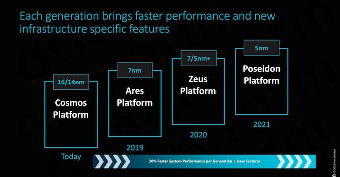
All of these new microarchitectures are important to Arm because they represent an inflection point in the market: Performance is now nearing that of the high-end players such as Intel and AMD, and Arm is confident in its ability to sustain significant annual improvements of 25-30% - vastly exceeding the rate at which the incumbent vendors are able to iterate.
The Server Inflection Point: An Eventful Last Few Months Indeed
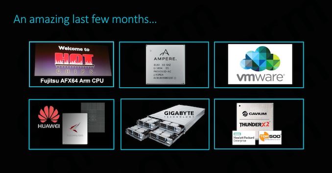
The last couple of months have been quite exciting for the Arm server ecosystem. At last year’s Hotchips we’ve covered Fujitsu’s session of their brand-new A64FX HPC (High performance compute) processor, representing not only the company shift from SPARC to ARMv8, but also delivering the first chip to implement the new SVE (Scalable Vector Extensions) addition to the Arm architecture.
Cavium’s ThunderX2 saw some very impressive performance leaps, making its new processor among the first to be able to compete with Intel and AMD – with partners such as GIGABYTE offering whole server systems solutions based on the new SoC.
Most recently, we saw Huawei unveiled their new Kunspeng 920 server chip promising to be the industry’s highest performing Arm server CPU.
The big commonality between the above mentioned three products is the fact that each represents individual vendor’s efforts at implementing a custom microarchitecture based on an ARMv8 architectural license. This in fact begs the question: what are Arm’s own plans for the server and infrastructure market? Well for those following closely, today’s coverage of the new Neoverse line-up shouldn’t come as a complete surprise as the company had first announced the branding and road-map back in October.
Introducing the Neoverse N1 & E1 platforms: Enabling the Ecosystem
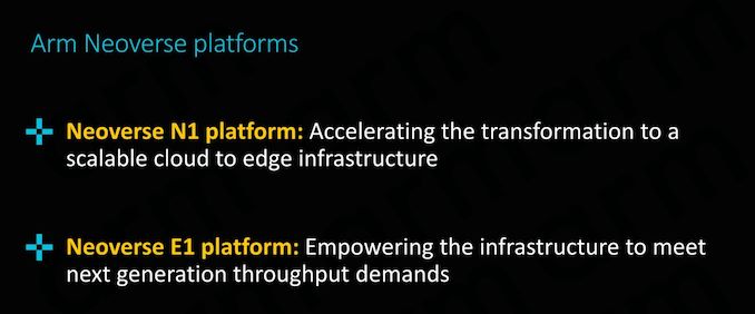
Today’s announcement is all about enabling the ecosystem; we’ll be covering in more detail two new “platforms” that will be at the core of Arm’s infrastructure strategy for the next few years, the Neoverse N1 and E1 platforms:
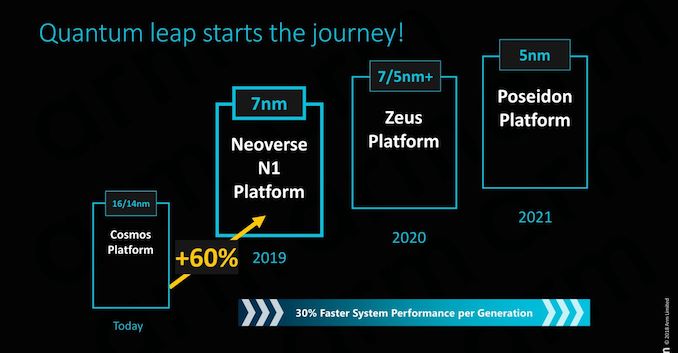
Particularly today’s announcement of the Neoverse N1 platform sheds light onto what Arm had teased back in the initial October release, detailing what exactly “Ares” is and how the server/infrastructure counter-part to the Cortex A76 µarchitecture will be bringing major performance boosts to the Arm infrastructure ecosystem.
The Neoverse N1 CPU: No-Compromise Performance
At the core of the Neoverse N1 platform is the Neoverse N1 CPU. First of all to get the naming matter cleared up: Yes the CPU branding will have the same nomenclature as the platform branding. What Arm describes as the platform is not only the CPU core but also the surrounding interconnect IPs that enables the whole system to scale up to a many-core system.
The Neoverse N1 Platform and CPU represents Arm’s first ever dedicated computing IP specifically designed for the server and infrastructure market. This is a major change to past IP offerings where the same CPU IP would be offered for both consumer products as well as industry solutions. This new technical distinction between the IP families is what drove Arm to adopt a new marketing name for the new infrastructure targeted products, and hence the Neoverse branding was born, differentiating itself from the consumer-oriented Cortex CPU branding.
As mentioned in the introduction, the Neoverse N1 platform represents the first iteration of a new family of microarchitectures coming out of Arm’s Austin design centre. The N1, formerly known as “Ares”, represents the sever core counter-part to the “Enyo” Cortex-A76 µarch. The Austin team has likely already finished work on Zeus (consumer variant: Deimos) and we’re expecting Poseidon (consumer: Hercules) to be the final iteration of this family before the torch is passed on to the next microarchitecture family, likely currently being worked on by the Sophia-Antipolis design team.
The N1 CPU micro-architecture
With the N1 CPU being the infrastructure sibling of the Cortex-A76, it’s natural that we see a lot of similarities between the two cores. We’ve had the pleasure to cover the A76’s µarch disclosure last year in detail, and much of what we’ve covered in terms of the inner-workings of the new micro-architecture will also apply to the N1, with some notable differences that adapt the core for infrastructure use-cases.
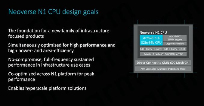
In terms of high-level design goals, Arm’s target seems to be fairly straight-forward: Create a no-compromise microarchitecture that will be able to serve as the foundation that will be iterated on in the next several years.
In particular one design goal that also mirrors what we’ve seen in the Cortex A76 is that Arm is tailoring the microarchitecture to be able to run at maximum frequency in infrastructure deployments. This is in contrast to the strategy that AMD and Intel are employing for their server CPUs, where the products may have the same or similar microarchitectures to their consumer counter-parts, however come with much more limited clock frequencies. The advantage here for Arm is that this allows them to simultaneously optimise performance, power and area all at the same time, while Intel and AMD might have to compromise in one of these metrics depending what market segment is targeted with a given SKU.
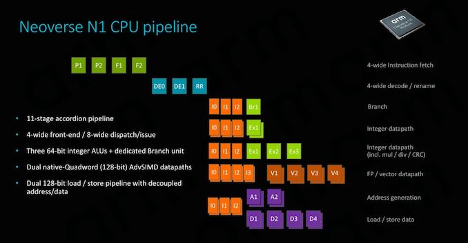
The N1 CPU shares the same pipeline organisation we’ve seen on the Cortex A76. At the heart, this is a 4-wide fetch/decode machine with a very short pipeline depth of only 11 stages. Arm calls this an “accordion” pipeline because depending on the instruction, it’s able to reduce the length down to 9 stages in latency-sensitive situations. The second predict stage is able to overlap with the first fetch stage, and the dispatch stage is able to overlap with the first issue stage, same as on the A76.
The execution back-end also looks largely identical to the Cortex A76: We have 2 simple ALUs, one complex ALU which handles complex operations such multiplications and division, and two full-width 128b SIMD pipelines which handle vector as well as floating point operations.
Data throughput is an important aspect of the microarchitecture and here Arm again sees the deployment of two 128bit load/store units, able to sustain sufficient bandwidth to feed and service the execution pipelines.
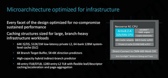
The front-end of the CPU continues on sharing similarities with the Cortex A76: we’re seeing large L1 and L2 with low latency access. Arm here also employs some of the biggest branch target and direction prediction buffers that are publicly known in the industry, showcasing a big focus on trying to improving performance not just by having a wide core, but rather by trying to keep data flowing through the core by minimising both branch as well as cache misses.
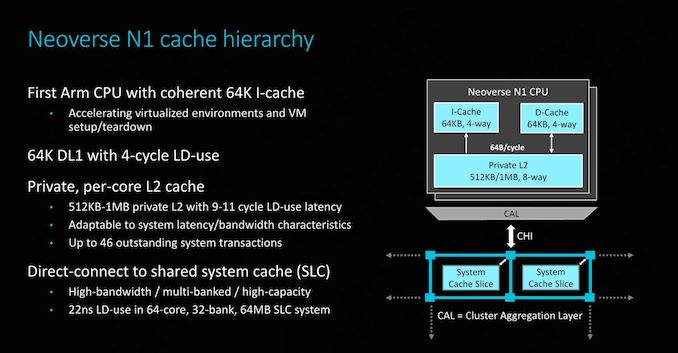
The cache hierarchy is one aspect where the N1 CPU differs more considerably from the A76. At the lowest level, the L1 cache still offers the same 64KB capacity with 4-cycle LD-use as its sibling, however the big important novelty on the N1 CPU is that now the cache is fully coherent. It’s noted that hardware I-cache coherency isn’t something that is required by the ISA and usually the way things have been done till now is through software maintenance operations. Getting hardware coherency implemented for the N1 was very important for Arm as it vastly improves performance and simplifies implementation of virtual environments, something that Arm needed to have if it wanted to be competitive among hyperscale customers. Having I-Cache coherency is noted to be a key enabler in order to scale the system for very large core-counts, and Arm describes it inherently a must-have for any system with a coherency plane of more than 16 cores.
The L2 cache is offered either in 512KB or 1MB options. The 512KB configuration matches what was available on the A76, while the addition of a 1MB cache likely targets heavier memory footprint applications in the infrastructure segment. It’s to be noted that doubling the L2 cache to 1MB doesn’t come without cost: the latency of the cache in this configuration sees a 2-cycle degradation, reaching a load-use latency of 11 cycles.
An immense difference to the Cortex A76 is when we go higher up the memory hierarchy. Instead of finding a cluster, the N1 CPU connects to a mesh interconnect. In particular we’re talking about Arm’s CMN-600 Coherent Mesh Network.
As depicted in the graph, this connection first follows through a CAL, or Component Aggregation Layer. Each CAL supports only up to two interfaces, which is why we only see two CPUs per “cluster” (it’s not really a cluster per se). The CAL then connects to an XP (Crosspoint) of the mesh, which essentially the switch/router component of the network. Each XP has two ports available; in the case of Arm reference design example the second port connects a SLC (System Level Cache) slice.
In an example configuration with 2MB SLC slices in a 64-core system (32 banks/slices), the average load-use latency for the whole 64MB cache would be 22ns. The reason that Arm gives the latency figures in ns rather than in cycles is because the SLC and mesh run on a different clock plane than the CPUs, usually at about 2/3rd the frequency of the cores.
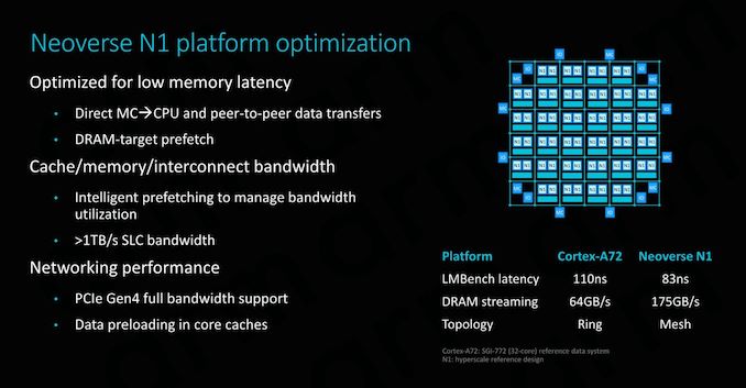
Direct connect is an integral feature of the N1 and the CMN-600. This is a feature that only exists on this platform and something that isn’t possible on Cortex CPUs. Essentially it removes all the L3 and snoop-filter logic of the DSU and instead it directly connects the CPU cores to the CMN’s CHI’s interfaces. Thus essentially communication between the memory controller and the CPU core only has to pass through one intermediate layer, which is the mesh network itself. This might sound like something obvious coming from a traditional PC and server CPU background, but it’s an important distinction to make considering Arm’s history coming from mobile SoCs where data transfers have to go through cluster-level logic first.
Direct MC -> CPU data transfers might be a bit of confusing term to explain. Here when a CPU makes a data-request to the MC (Memory controller), it’s able to immediately and concurrently first send a “prefetch” type request directly to it, while at the same time the normal transfer command goes through the snoop-filter of the home-node of the XP in the mesh network, and then routing the request to the memory controller. Thus the MC will know in advance the request is coming and will have already started to get the data, hiding part of the effective memory latency than if the whole transfer would have happened in serial sequence.
Prefetching is extremely important to the performance of the whole system, and here data prefetching is intelligently managed to optimise system-level bandwidth.
In the example N1 reference system with 64 cores and 8 DDR-3200 memory channels, the N1 is said to achieve up to 175GB/s of DRAM streaming bandwidth. Arm also publishes latency numbers, but it’s to be noted that it’s a bit hard to make direct comparisons: Arm’s figures represent LMBench figures while configured with 2MB hugepages at a 256MB test depth. The choice of hugepages reduces TLB misses and gets nearer to the actual memory latency, and this was the rationale behind Arm publishing the metric under these circumstances.
We haven’t had the opportunity to test competing systems with hugepages enabled, but an AMD’s Epyc 7601 (LRDIMM DDR4-2666 19-19-19) will achieve ~73ns with an LMBench-like test at the end of the chip’s cache hierarchy, while a custom developed latency test minimising TLB misses to a minimum showcases a DRAM-load-use of around 57ns. An Intel W-3175X (RDIMM DDR-2666 24-19-19) system under the same tests achieved respectively 94ns and ~64ns. Again it’s hard to come to any hard conclusions here and the metrics aren’t directly comparable to Arm’s figures - we’d have to see a full latency curve of different tests to better determine things.
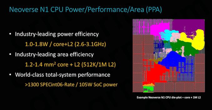
The N1 CPU when implemented on a 7nm TSMC process remains an extremely tiny piece of silicon. For an implementation with 512KB L2 cache Arm discloses a die size of 1.2mm², nearly identical the 1.26mm² footprint we measured a Cortex A76 on the Kirin 980. Doubling the L2 cache to 1MB raises the footprint by 0.2mm² to 1.4mm² per core.
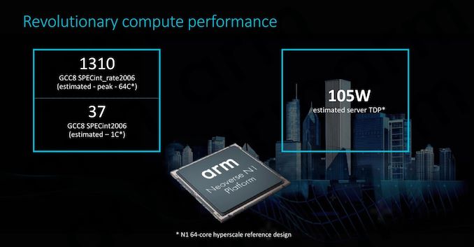
In terms of frequency range, Arm envision 2.6GHz to 3.1GHz. The lower figure is quoted at a process nominal voltage of 0.75V while the 3.1GHz figure is under overdrive at 1V. It’s to be noted that the 19% higher frequency would come with a 44% higher power cost, so most vendors will want to stay nearer to the more efficient part of the power curve. In absolute figures, this is still only 1.0 to 1.8W. 1W gives plenty of headroom for a 64-core SoC while still remaining under some impressive total SoC power levels. Here Arm’s 64C N1 reference design would come at a total power budget of around 105W. We’ll be addressing the performance figures on the next page.
N1 Hyperscale Reference Design
A big part of what is defining the N1 Platform as an actual platform, is the fact that Arm is offering a full reference design with a set of IPs that is fully validated by Arm themselves.
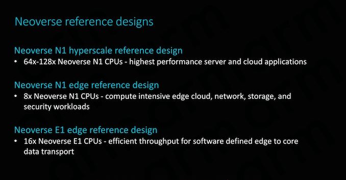
Here we see three reference designs, a Neoverse N1 hyperscale design, which we’ll get into more detail shortly, an N1 edge design, and a Neoverse E1 edge design. Arm’s goals with the reference designs is to give vendors “sweet-spot” configuration options that they will then be able to implement with (relatively) minimal effort.
The N1 hyperscale design is what we’ll be covering in more detail as this represents Arm’s most cutting-edge and competitive product.
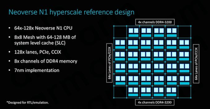
As covered on the previous page, at the heart we find the Neoverse N1 CPU in either 64 or 128 core configurations, integrated in a CMN-600 mesh network with either 64 or 128MB of SLC cache. We also see 128 lanes for PCIe 4 respectively CCIX interfaces which provide plenty of I/O bandwidth.
In terms of memory controllers, Arm employs 8x DD4 interfaces up to 3200MHz. Arm actually has abandoned development of its own memory controllers as customers in most cases opted for their own in-house designs or rather opted to choose IP from other third-party vendors such as Cadence or Synopsys. For the current reference designs Arm’s own DMC-520 was still up-to-date and a well-understood block for the company, although in the future newer memory controllers such as for DDR5 will have to rely on third-party IP. Naturally, the reference design targets the latest 7nm process node.
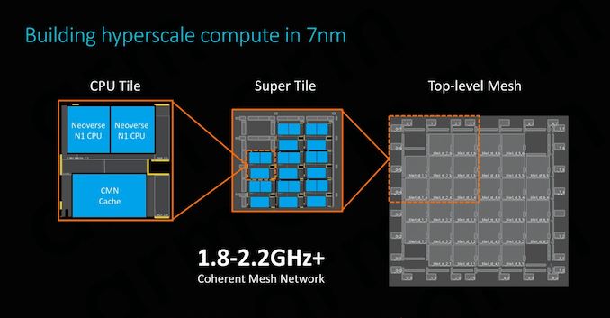
The physical implementation of the SoC would use replicable hierarchical building blocks for ease of design. A “CPU Tile” consists of the two N1 CPU cores, a slice/bank of the SLC cache as well as part of the CMN’s cross points and home-nodes. This CPU Tile is replicated to generate a “Super Tile”, what is added here is peripheral parts of the SoC such as I/O as well as memory controllers. Finally, replicating the super tile in flipped and mirrored implementations results in the final top-level mesh that is to be implemented on the SoC.
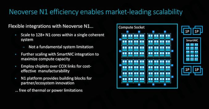
Scaling the design to 128 cores doesn’t represent an issue for the IP, although we’ll be hitting some practical limits in terms of current generation technology. Arm’s 64 core N1 reference design with 64MB of cache on a 7nm process node would result in a die size a little under 400mm², which probably is on the higher end of what vendors would want to target in terms of manufacturability. To alleviate such concerns, Arm also took a page out of AMD’s book and floated the idea of chiplet designs, where each chiplet would communicate over CCIX links. Inherently it’s up to the vendor to decide how they’ll want to design their solution, and Arm provides the essential building blocks and flexibility to enable this.
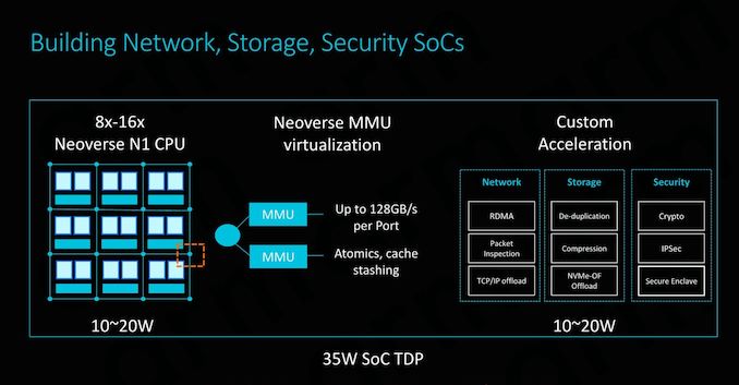
SmartNIC integration capability is also an important aspect of the design and its flexibility. To maximise compute capacity in large scale system, having accelerated network connectivity is key in actually achieving high throughput in the densest (and efficient) form-factor possible.
The CMN-600 allows for slave ports on its crosspoints: Here we can see MMUs connected with high bandwidth interfaces of up to 128GB/s. Attaching fixed-function hardware offloading IP thus would be extremely easy to implement.
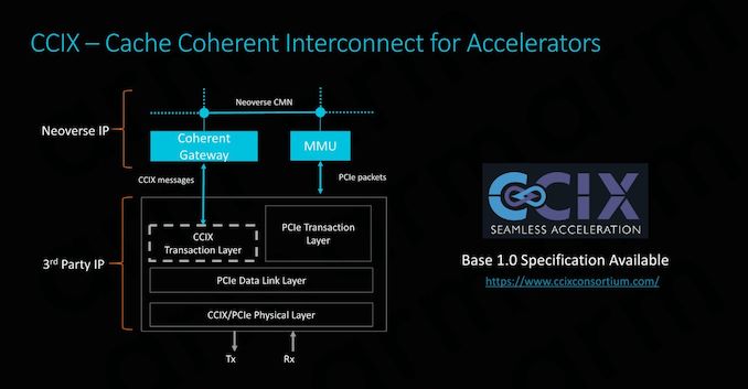
CCIX is extremely important for Arm as it enables its product portfolio to integrate with third-party IP offerings. Enabling cache coherency for external IP blocks is an incredibly attractive feature to have as it massively simplifies software design for the vendors. Essentially what this means is that software simply sees a single huge block of memory, whereas non-coherent systems require drivers and software to be aware and track what part of memory is valid and what isn’t. In terms of IP integration, Arm provides the CCIX coherent gateway that integrates with the CMN-600, while on the other side it’s the onus of the third-party IP provider to provide the CCIX translation layer.
Currently Xilinx will be among the first vendors to offer CCIX-enabled end-products in Q3 2019. With AMD also fully embracing CCIX, there’s some very exciting future potential for third-party accelerator hardware, and we be seeing new use-cases that just weren’t feasible before.
Power/Performance management
While it’s a bit weird to talk about power management in the context of implementation scalability (The average reader might think of it as a thermal/cooling consideration), there’s some very interesting implications in terms of how Arm simplifies the work needed to be done by the vendor.
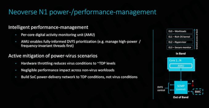
Along a chip’s logical design, a vendor must also implement a power delivery network that will be able to adequately support the IP. In real-world use-cases this means that the PDN needs to be as robust as to deal with the worst-case power scenario of a component. This is actually quite a headache for many vendors as the design requires complex models and in most cases the PDN will need to be over-engineered in order to offer guarantees of stability, which in turn raises the complexity and cost of the implementation.
Arm seeks to alleviate these concerns by offering extremely fine-grained DVFS mechanisms in the form of a dedicated micro-controller. The controller access detailed activity monitoring units inside the CPU cores, seeing what actual blocks and how many transistors are actually actively switching, and feeding this information back to the system controller to change DVFS states. This provides a certain level of hard-guarantee as to when the CPU enters power-virus-like workloads which can cause current spikes, and avoid them in time. This enables vendors to design their PDNs to more conservative tolerances, saving on implementation cost.
Performance Targets: What Are The Numbers?
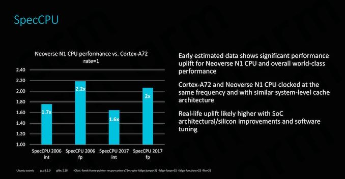
Naturally all this talk about performance and efficiency needs to substantiated with some concrete numbers. In the context of today’s announcement, most performance figures disclosed by Arm were relative improvements compared to the A72 Cosmos platform, which might not be the most relevant data-point in terms of trying to actually place the N1 in the competitive landscape, however we also have some more concrete absolute figures we’ll try to put some more context behind shortly.
The comparison to the A72 at the same frequency as well as a similarly configured system with SLC configuration, the new N1 outright smashes its predecessor platform / microarchitecture. The figures here represent single-threaded performance in SPEC. In integer workloads we see PPC (performance per clock) and absolute performance gains from 60 to 70%. The floating point benchmarks are even more impressive with gains ranging from 100 to 120%. The data-points represent modelled and emulated performance estimates, the actual real-life performance improvements will higher due other SoC-level improvements as well as software improvements that aren’t available in existing actual A72 silicon products.
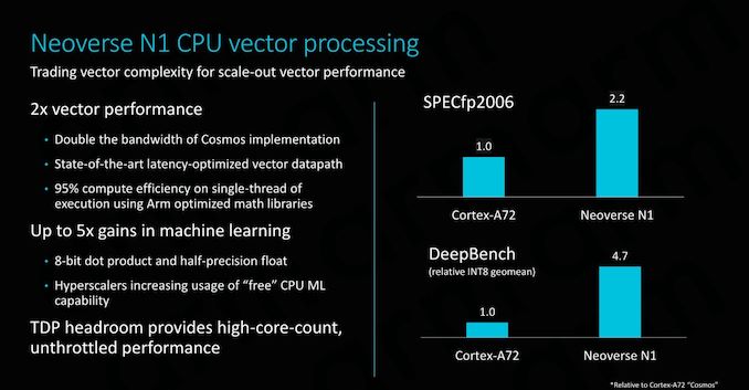
Arm again iterates the very large compute performance improvement compared to existing solutions, achieving beyond 2x performance boosts in vector workloads. Naturally, the N1’s ARMv8.2 ISA implementation also means that it supports 8-bit dot product as well as FP16 half-precision instructions which are particularly well fitted for machine-learning workloads, achieving performance boosts near 5x the predecessor platform.
Overall, Arm’s comparison to the A72 makes sense in the context that this is to its predecessor, however we have to keep in mind that the Cortex A72 was a core that was first introduced back in 2015 with first silicon products being released late that year as well as 2016, while the new Neoverse N1 in all likelihood isn’t something which we’ll be seeing in products for another 12-18 months, resulting in a ~3-4 year time span between the two products.
Arm did also divulge absolute SPEC numbers, and here we can have some more interesting analysis to competing platforms:
For a Neoverse N1 64-core hyperscale reference design running at about 2.6GHz, Arm proclaims single-threaded SPECint2006 Speed score of ~37 while reaching an estimated multi-threaded scores of 1310. The figures here are achieved in a quite low whole-server TDP of only 105W. The figures weren’t run actual silicon but rather estimated on Arm’s server farm in an emulation environment with RTL.
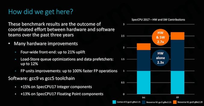
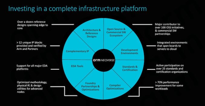
Arm made a big note that among the many efforts to improve performance for the Arm ecosystem isn’t only offering better hardware, but also better software. Over the last few years Arm has put a lot of effort into improving open-source tools and compilers, such as GCC. Comparing the latest GCC9 version to GCC5, we’re seeing improvements of 15-13% in integer and floating-point workloads. It’s to be noted that the optimisations made here are real-world use-case improvements, and not targeted changes that are meant to improve SPEC scores.
In order to put context around Arm’s numbers, I went ahead and compiled a set of binaries with GCC8 and had Ian run it on Intel’s and AMD’s latest and greatest, an Xeon W-3172X as well as a AMD Epyc 7601. It’s to be noted that the compiler flags weren’t exactly the same – both AnandTech’s and Arm’s builds were running under –Ofast, however Arm also added some minor flags which I hadn’t had the chance and time to cross-check, as well as enabling LTO. I’m not too concerned about the flag variations, however LTO will give Arm a 2-3% performance advantage over our internal numbers. It’s also to be noted that Arm’s single-threaded figures are marked as “Peak” scores, meaning each individual workload was run with the best performing compiler flags, while our internal figures are “Base” scores, meaning we’re running the same flags across all binaries and tests.
Edit: 25/02/2019: Arm have reached out to clarify that the performance scores were in fact Base runs and without LTO - the slides in question were mixing things up. Thus we have proper apples-to-apples comparisons in our numbers versus Arm's internal numbers.
As always we have to disclose that the below figures are merely internal estimates as they’re not official SPEC submissions. SPEC CPU 2006 has also been deprecated in favour of SPEC CPU 2017. Arm stated that they’ve shared SPEC CPU 2006 figures as that’s still the industry standard at the moment which gives users and customers the best context, and in the coming year or so they’ll switch over to also sharing SPEC CPU 2017 numbers. As for us at AnandTech, I’ve prepared SPEC CPU 2017 and Ian and I will be adopting it in our benchmark suites for PC/server CPUs as well as mobile SoCs in the coming weeks and months.
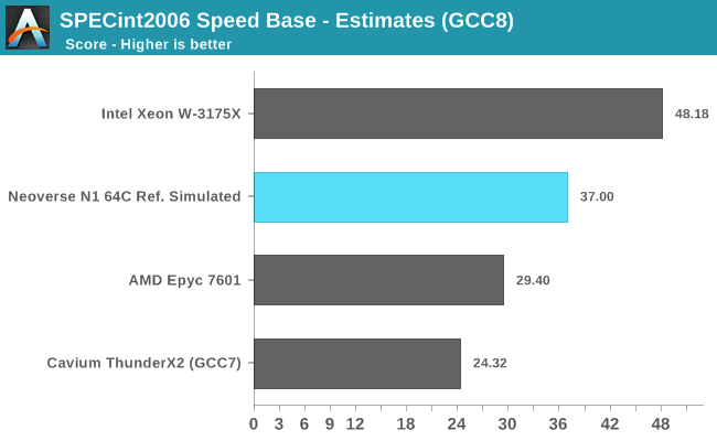
In terms of single-threaded performance, the N1 looks to be outright outstanding. With an estimated score of 37, it would beat the most recent and best-performing Arm server CPU, Cavium’s ThunderX2, by a significant margin. It’s to be noted that the real-world performance difference would be smaller than depicted in the above figures: GCC8 notably improved loop vectorisation in 456.hmmer which will give it a 1-2% overall score boost, and of course we have to take into account 2-3% difference due to Arm’s different compiler flags.
Intel’s W-3175X is hardly the most representative hyperscaler CPU, however it gives context as to what Intel’s top-end single-threaded performance in their best multi-core CPUs is. As a reminder, the W-3175X has a single-threaded boost clock of 4.5GHz, significantly above what we see in server SKUs such as the Xeon 8180. AMD’s Epyc 7601 is a more representative data-point against what a hyperscale design such as the N1 would compete against, again as a reminder this is a 3.2GHz single-threaded boost clock on the part of AMD’s first generation Zen core.
What surprised me the most about Arm’s quoted ST score of ~37 is that it’s significantly higher than what we measure on the Cortex A76, which scores in at about ~26 on actual hardware. Software and compiler considerations aside, one of the explanations for this huge 42% performance discrepancy could be the N1’s much better memory and cache system. Here the full system bandwidth is 6x higher than on mobile SoCs, and naturally in a single-threaded workload the thread would have full access to the Neoverse’s N1 64MB SLC cache, a whopping 16x bigger than the L3 in current mobile Cortex A76 designs. If the performance difference is indeed explained by the memory subsystem, it just gives to explain just how important it is to the performance scaling of a core.
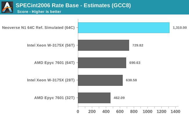
Switching over to multi-threaded workloads represented by SPECrate2006, we have to note that this is a best-case scaling scenario for all platforms as there is no serialisation or inter-thread communication, as the test suite simply runs multiple processes in parallel. Even with this in mind, Arm’s projected results for a N1 64 core design are just outright impressive considering the fact that we’re talking about TDPs much smaller than any of AMD and Intel’s solutions, creating a performance and efficiency gap that I have a hard time seeing the x86 solutions being able to compete against.
We have to remember that we’re comparing a 64 core platform against AMD and Intel’s current 32/28 core platforms. A more fair comparison would be AMD’s upcoming Rome with 64 CPU cores, here even if AMD manages to outright double multi-threaded performance and match Arm’s projected MT numbers, I don’t see them be able to at the same time lower the TDP to match Arm’s estimated 105W target (The Epyc 7601 has a TDP of 180W, Rome details haven’t been announced yet).
SPEC’s Rate benchmarking scoring scales linearly with the instance count. In this case, if we divide Arm’s 1310 figure by the 64 cores of the system, we get a per-instance score of around ~20.5, which seems much more realistic and in-line with the Cortex A76 results we measure on current mobile devices.
Arm’s performance predictions for the Cortex A76 were quite spot on to what we measured on actual devices. We thus are more inclined to give Arm credence and the benefit of the doubt in regards to today’s projected Neoverse N1 scores. The figures do make sense, and are in line with what we saw the microarchitecture able to achieve in mobile.
Naturally we shouldn’t come to any conclusion until we actually have the actual hardware in our hands, but the presented figures are certainly promising if they can be realised by vendors implementing Neoverse N1 systems.
The Neoverse E1 CPU: A Small SMT Core for the Data-Plane
We’ve talked a lot about the Neoverse N1 – but today’s announcement actually covers two new platforms. Today actually isn’t the first time that we’ve talked about the other new platform, the new Neoverse E1. Codenamed Helios, the E1 CPU actually is derived from the Cortex-A65AE which we’ve already briefly talked about in December.
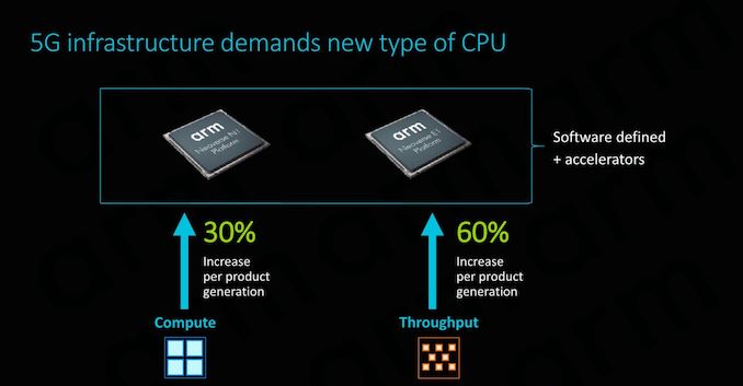
Arm largely differentiates between two big workload types in infrastructure deployments, “Compute” use-cases where we need arithmetically capable CPU cores such as the N1, and “Throughput” workloads that largely are mainly about shifting large amounts of data around. The latter category is what the new Neoverse E1 is targeting, representing a specialised CPU core that efficiently and cost effectively is able to handle such tasks.
Arm’s First SMT Core
As some might have read in the Cortex-A65AE announcement piece, the µarchitecture used in Helios both in the Cortex chip as well as in the Neoverse E1 represents Arm’s first ever foray into designing and bringing to market an SMT (simultaneous multi-threading) core. It may at first glance sound a bit weird to have SMT introduced in a smaller CPU core, as traditionally we would be thinking about SMT being useful in raising the back-end execution unit utilisation rate in larger microarchitectures, but it actually makes a lot of sense as well in smaller CPU cores whose workloads are predominantly in the data plane.
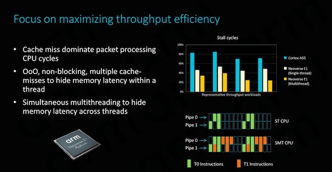
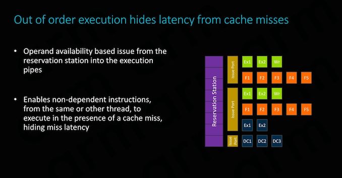
In data-processing workloads, cache misses dominate CPU work cycles. This is because we’re talking about data that inherently doesn’t have a long residence time on the CPU core, either streaming from sensors as described in the use-case of the Cortex-A65AE, or in this case streaming from the network in the case of infrastructure workloads. This means that the CPU has to deal with long memory latency accesses, introducing stalls in the CPU pipelines.
The E1 CPU is a small out-of-order design with SMT: In data-plane heavy workloads, introducing the ability to handle a secondary thread on the CPU core essentially represents almost a free throughput gain for the microarchitecture, as it’s able to fill unused execution cycles that otherwise would have just gone to waste. Indeed in optimal workloads, this can result in essentially a doubling of the throughput, on top of the single-threaded microarchitectural gains that the E1 CPU brings over predecessors such as the Cortex A55.
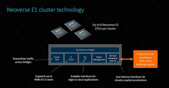
At the cluster level, the Neoverse E1 CPU configuration options are extremely similar to what we’ve seen deployable in DynamIQ systems. The cluster itself looks very much like a DSU, with up to eight cores, a cluster-level snoop filter, and an L3 cache configurable up to 4MB.
The E1 CPU’s Pipelines
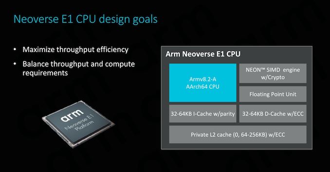
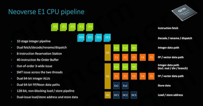
The E1’s CPU pipeline actually represents a brand new-design which (besides the A65) haven’t seen employed before. What Arm has done here is take the foundation of what was the in-order Cortex A55 µarch and turned it into a minimally narrow out-of-order CPU. Moving to a basic out-of-order CPU design was essential in order to get more throughput out of the core, as it avoids stalling the whole pipeline in scenarios where we’d have a long load.
The fetch/decode/dispatch stages of the pipeline is 2-wide. In terms of its out-of-order windows, we see a small 40-deep ROB (Re-order buffer).
On the back-end we find a similar execution unit count and layout as on the Cortex-A55. A big difference to the A55 is that the integer ALUs are now differently partitioned: One ALU is dedicated for simple arithmetic operations only, while the second unit now takes over both integer multiplication as well as division tasks, whereas this was divided among the two ALUs in the A55. Interestingly, Arm also demarks the branch port being shared with this second complex integer ALUs, no longer representing it as a dedicated port as on the A55.
The SIMD/Neon pipelines seem to remain the same as on the A55 in terms of its high-level capabilities, but it is possible Arm may have improved cycle latencies of some instructions between the two generations.
Finally, the load and store ports also match the capabilities of the A55.
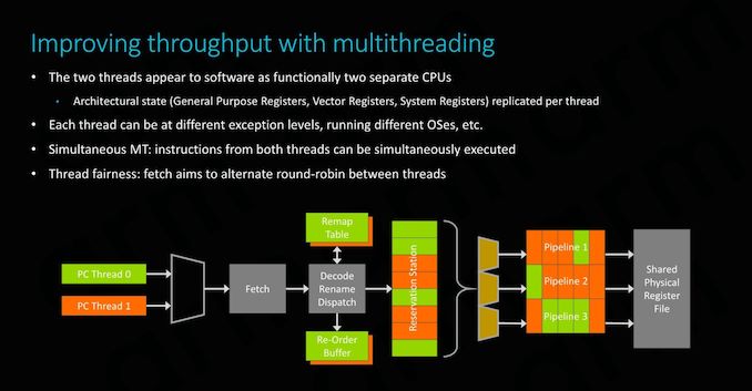
SMT on the Neoverse E1 is enabled through the duplication of architectural state components of the core. This means the CPU has double the general purpose, vector and system registers and their corresponding structures on the physical core.
At the software level, this naturally simply appears as two separate CPU cores, and can be run at different exception levels or even be running different OSes.
Performance partitioning between the two threads is enabled by a simple round-robin instruction fetch mechanism, ensuing that both threads get the same amount of attention.
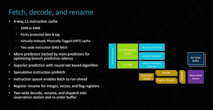
The front-end of the CPU has seen improvements in all regards and adopts many of the state-of-the art front end branch prediction and prefetch mechanisms we find in other more recent Arm OoO cores – just in a more limited implementation optimised for the smaller nature of the E1 CPU.
As mentioned just earlier, although the throughput of the execution pipelines hasn’t fundamentally changed, Arm has updated the execution units to employ newer designs with shorter cycle latencies. Here in particular FMAC latency has bene halved, while the integer division unit has been updated to a Radix-16 unit. It’s to be noted that these improvements are again slightly misleading as Arm is making comparisons to the Cortex A53 – the newer Cortex A55 already employed the aforementioned changed, including the new ARMv8.2 double throughput FP16 instructions as well as Int8 dot-products.
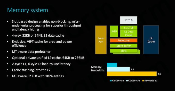
On the memory system side of things, we again see very large similarities to the Cortex A55 and the E1 enjoys the same improvements made by that µarch. The only other notable changes here are the fact that the data prefetchers as well as the L2 TLB are now multi-thread aware and are optimised in their design to better operate with the new SMT nature of the core.
E1 Implementation & Performance Targets
The Neoverse E1 CPU being a small CPU core aimed at cost-effective and dense implementation naturally needs to be quite small, as well as power efficient.
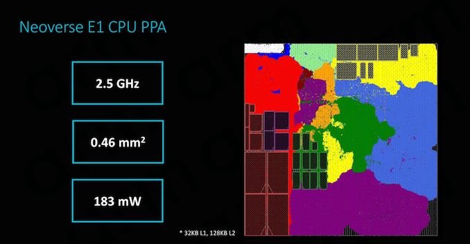
Implemented on a 7nm process, Arm physical design team is able to get an E1 CPU core with 32KB L1 and 128KB L2 cache down to 0.46mm² - all while reaching a high clock of 2.5GHz and a power consumption of 183mW. The higher clock was a surprise as it is quite notably higher than what we’ve seen vendors achieve on the A55 – although we are talking about different implementation targets.
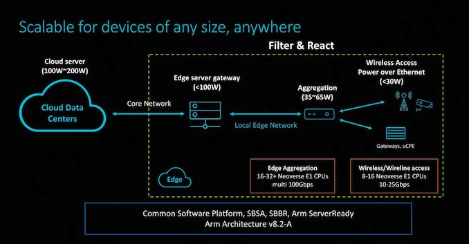
Arm envisions the most popular implementations of the E1 to be found in lower power edge applications. At the lower end, ranging from 8-16 cores would be a good for wireless access points and gateways, delivering data throughputs in the 10-25Gbps rang. A tier up we would see 16-32 core designs in use-cases such as edge data aggregation deployments, achieving data rates in the 100’s of Gbps.
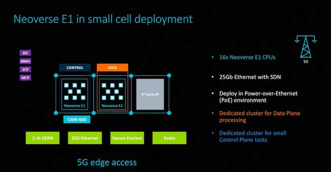
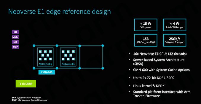
The Neoverse E1 reference design that Arm offers and sees as being the most popular “sweet-spot” is based on a 16 core design. Here we have to clusters of 8 cores in a small CMN-600 2x4 mesh network, allowing for system cache options as well as integration of possible additional third-part IP. The envisioned memory system would be a 2-ch DDR4 configuration.
Such as SoC would have a power consumption of less than 15W, of which less than 4W would actually be used by the CPU cores. SPECint2006 rate scores would come in at 153 – which given the actual size and power consumption of the platform is quite impressive. The system would also be capable of 25Gb/s network throughput, enabled solely by a software transport layer (Meaning no hardware acceleration).
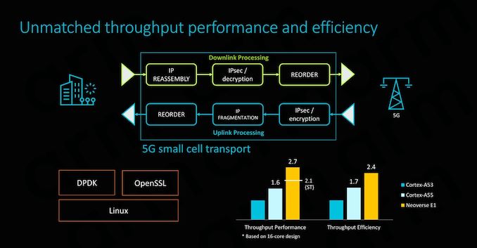
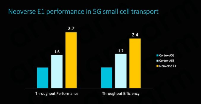
On a per-core comparison to the Cortex A53 and A55, the new E1 CPU would again offer significant throughput performance benefits, but also very importantly it would represent an efficiency boost compared to its predecessors (ISO process comparison).
First N1 Silicon: Enabling the Ecosystem with SDPs
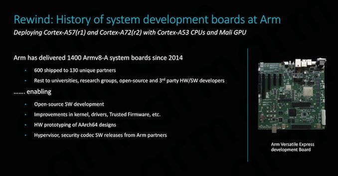
A little known fact about Arm is that the company designs its own silicon test platform – actually deploying them on development board to enable validation and software development on hardware that Arm and developers have full control of. The latest generation was the Juno platform, which in its first revision started off with a Cortex A57 and served as the fundamental silicon testbed for ARMv8 software.
Ever since Arm started the programme in 2014, Arm has shipped over 1400 boards both internally and to its partners. The amount of chips we’re talking about here sounds paltry, however we have to keep in mind we’re talking about very limited shuttle runs on MPW (multi-project wafers) where Arm shares wafer space with numerous other companies.
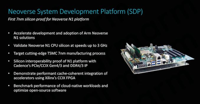
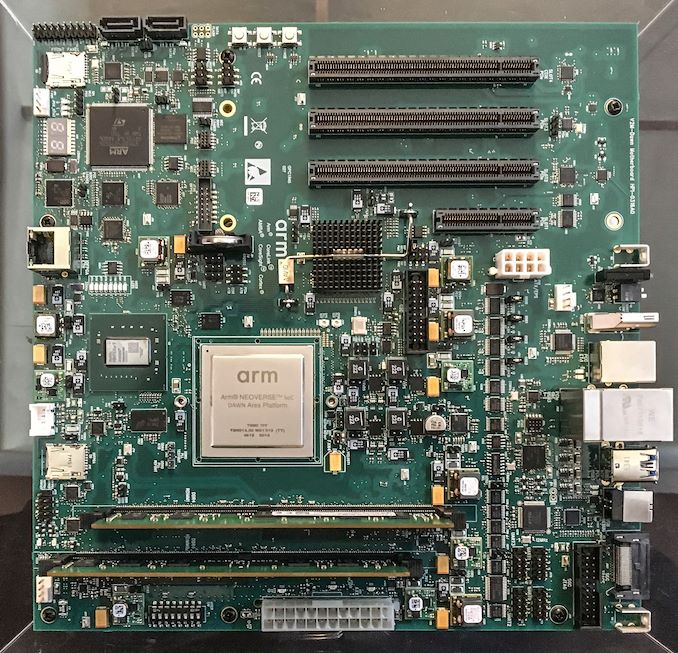
For today’s announcement, Arm had the pleasure to reveal that it received back the first working Neoverse N1 silicon back in December – with the chips meant to be integrated into the new Neoverse System Development Platform (SDP).
The N1 SDP represents major step for Arm as it not only is the first silicon to come back with the N1 CPU, but also is Arm’s first own 7nm silicon. The platform represents a major proof of concept of the IP, as well as interoperability with third-party IP, employing a lot of the peripheral IP such as PCIe and DDR PHY supplied by Cadence.
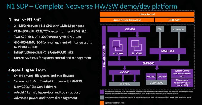
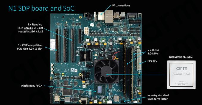
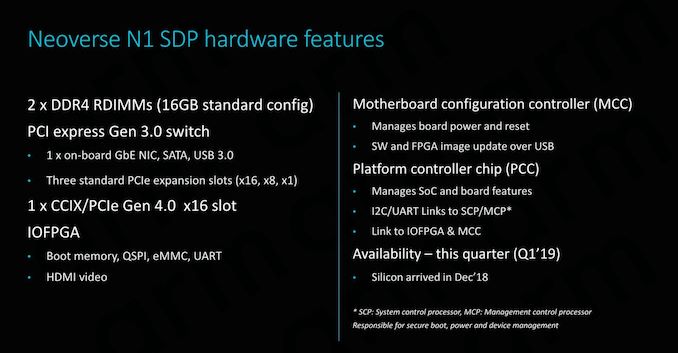
The actual hardware is a limited implementation of an N1 SoC – we find a 4-core N1 CPU with 1MB L2 configuration in the form of 2xMP2 connected to a CMN-600 with an 8MB SLC setup.
The board includes a CCIX compatible PCIe 4.0 x16 slot which serves the crucial role of enabling development and demonstrating cache-coherent integration with CCIX hardware such as Xilinx’s FPGA.
The N1 SoC actually doesn’t contain dedicated I/O IP, rather Arm implements all connectivity via a dedicated FPGA which serves as the I/O hub, supporting various connectivity options such as Ethernet, USB, SATA and so on.
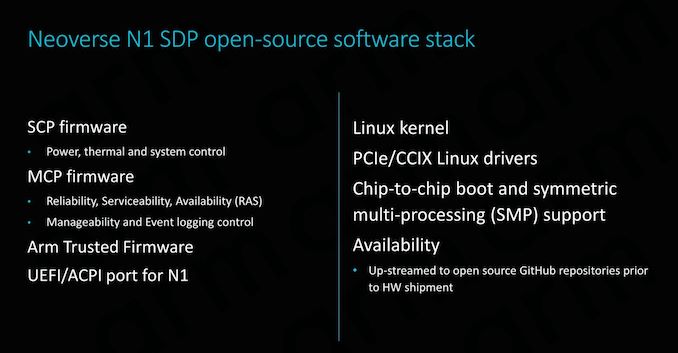
Naturally the big selling point of the SDP is its completely open-source firmware stack from not only the OS drivers, but more importantly the SCP and MCP firmware.
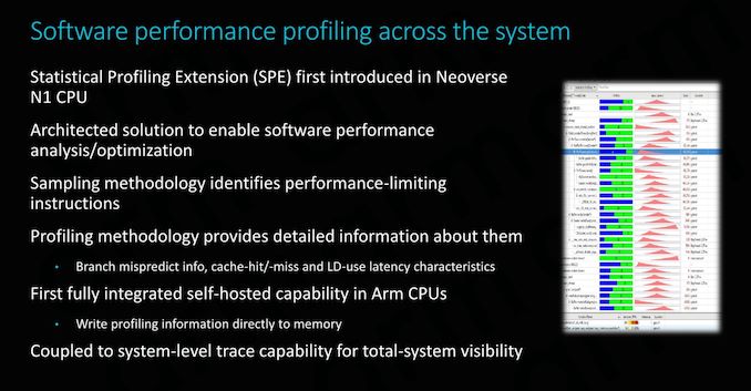
An important new feature that is first employed by the new N1 CPU is the introduction of statistical profiling extensions (SPE). The new extension enables the first ever self-hosted profiling capability in an Arm CPU – meaning we don’t require a separate CPU or system having to read out microarchitectural counters. Instead the new SPE can be configured to directly write this information into memory. The tool is extremely useful for tracing code and analysing core behaviour, identifying possible performance issues and further squeezing out the maximum performance out of a platform, something Arm is taking very seriously if it wants to succeed and gain adoption in HPC.
Finally, the N1 SDP will be available later this quarter – although don’t expect the board to be easily attainable for the average user.
End Remarks: Strengthening the Infrastructure Ecosystem
If there’s one thing that readers should take away from today’s presentations, it’s the fact that Arm is taking the infrastructure and server push extremely seriously. The last year in particular has been transformative for the Arm ecosystem as we’ve for the first time seen Arm vendor platforms be competitive with the major incumbents such as Intel and AMD.
The elephant in the room is Amazon, and last year’s reveal of a new AWS instance based on their own-in house ARMv8 Graviton processors marked a significant moment showcasing that Arm is now irrefutably becoming mainstream in the industry.
While Arm did not divulge any information on who will be employing the new Neoverse N1 platforms first – I would not be surprised if the next generation Graviton processor will based on the N1 CPU.
The N1 CPU looks to be an excellent CPU that targets a sweet-spot point between peak compute performance, overall throughput. And most importantly it maintains the leading power efficiency that is already found in Arm's mobile products. Arm has high hopes for N1 and its eventual successors, and for good reason: they're looking to steal market share away from the likes of Intel (and x86 servers in general), which has proven to be an entrenched market full of very high performance processors. For that reason Arm is bringing their best to the table, and while N1 isn't going to be a core-for-core competitor with flagship x86, it stands to pose a significant threat, especially in workloads that can easily scale up to a larger number of cores.
Meanwhile the new E1 CPU targets the expanding market for high throughput processors, which with the upcoming shift to 5G will require more throughput performance at low power levels. Here Arm seems to have custom-tailored a CPU specifically to serve such use-cases. This is a move that's arguably less about stealing market share from any one player, and more about being in the right place at the right time to secure their place in what should be a rapidly growing market. In that sense the E1 is a very traditional Arm move – focus on cost and simpler processors – and this has been a move that's continued to serve Arm well over the years.
Although the new hardware IP is impressive, what also matters greatly is Arm’s efforts into strengthening the Arm software ecosystem. Working with various industry hardware and software partners in trying to facilitate the software stack and interoperability with Arm not only benefits vendors using Arm’s own hardware IP, but also vendors who chose the route of employing their own custom CPU and SoC designs. Similarly, those vendors who are trying to improve and strengthen their own products will inevitably feed back into strengthening the Arm ecosystem as well – creating essentially what is a group effort between many companies that in the future will continue to gain momentum.
It's said that the Neoverse N1 will be commercially deployed by partners in the next 12-18 months, and I think this will be a crucial moment for Arm and the company’s server endeavours. If the major breakthrough in mind-share hasn’t already happened, if all goes well and Arm and partners deliver on the promised improvements, the next 1-2 years will certainly represent a major shift in the industry.

