Original Link: https://www.anandtech.com/show/13941/smics-14-nm-mass-production-in-1h-2019
SMIC To Start 14nm Mass Production in H1 2019
by Anton Shilov on February 8, 2019 1:00 PM ESTReports have emerged this week that SMIC, the largest foundry in China, is set to start mass production using its in-house developed 14 nm FinFET manufacturing technology in the first half of this year. Notably, this comes at least a couple of quarters earlier than was initially expected, indicating that SMIC is apparently ahead of schedule. Meanwhile the company is already working on its post-14nm processes, as development of its 10 nm and EUV-enabled 7 nm fabrication processes are currently underway.
Based on various reports from China and Taiwan technical media, SMIC’s yields at 14 nm have reached 95%, which is more than sufficient to start mass production. Consequently, the foundry is gearing up for volume production of a 14 nm smartphone SoC in the first half of 2019. While SMIC naturally does not disclose name of their first 14nm customer, the company’s key clients are HiSilicon, Qualcomm, and Fingerprint Cards (FPC, which produces fingerprint sensors), so it's a relatively short list of potential candidates.
Analysts say that SMIC’s 14 nm capacity will be relatively small when compared to the industry leaders, all of whom run multiple leading-edge fabs. SMIC currently has two fabs that can process 300 mm wafers using 28 nm and larger fabrication processes. The same fabs will be used for 14 nm projects too, but given their capacities and SMIC’s very high fab utilization rate (94.1% in Q2 2018), do not expect them to make loads of 14 nm SoCs. And for these reasons, along with prepping 14nm for its current fabs, the company is building a large $10 billion fab that will be used for its leading-edge manufacturing technologies in the future.
“SMIC is getting $10 billion to build capacity for 14nm, 10nm and 7nm. They will have capacity for 70,000 wafers a month by Q4 in 2021,” said Handel Jones, chief executive of International Business Strategies (IBS). “The building is huge. They have bought some equipment, but nothing significant yet.”
That said, do not expect SMIC to produce SoCs using leading-edge FinFET process technologies in quantities that are comparable to other makers of semiconductors in the foreseeable future. Even if the company can line up the capacity, lining up the demand could prove trickier. 14 nm chips are expensive to design and build the masks for, which is why so much chip volume is still at 28 nm and larger
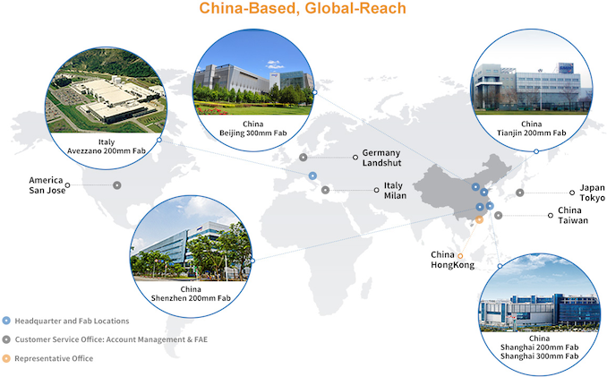
| Overview of SMIC's Fabs | ||||
| Process Technologies | Capacity Wafer Starts per Month |
Location | ||
| BJ | 200mm | 90 nm - 150 nm | 50,000 | Beijing, China |
| 300mm | 28 nm - 65 nm | 35,000 | ||
| SH | 200 mm | 90 nm - 350 nm | 120,000 | Shanghai ,China |
| 300 mm | 28 nm - 65 nm | 20,000 | ||
| SZ | 200 mm | 90 nm - 350 nm | 60,000 | Shenzhen, China |
| TJ | 200 mm | 90 nm - 350 nm | 50,000 | Tianjin, China |
| LF | 200 mm | 90 nm - 180 nm | 50,000 | Avezzano, Italy |
SMIC's latest progress slots in well with China's ambitious “Made in China 2025” plan. Under the plan, government planners want to achieve a 70% chip self-sufficiency by 2025, which having a leading-edge fab will help with. However there's doubt among analysts doubt that it is possible. Most of the ICs produced in China by 2025 will be made by companies based outside of the country.
Past 14nm, SMIC is already at work on its 10nm and 7nm processes as well, as previously confirmed by the company in 2018. Both processes are extremely costly to design, but since the semiconductor industry is growing in general and because of generous funding from the Chinese government (and various affiliated parties), SMIC has enough money for the necessary R&D. Working towards that goal, last year SMIC acquired an EUV step-and-scan system from ASML for $120 million, which is expected to be delivered early in 2019 for use in 7 nm process development and eventually mass production.
Related Reading:
- GlobalFoundries and Chinese Authorities Reconsider Plans
- Intel to Expand Production Capacities at Multiple Fabs
- Intel: EUV-Enabled 7nm Process Tech is on Track
- TSMC: 7nm Now Biggest Share of Revenue
- Samsung Starts Mass Production of Chips Using Its 7nm EUV Process Tech
- GlobalFoundries Stops All 7nm Development: Opts To Focus on Specialized Processes
- TSMC: First 7nm EUV Chips Taped Out, 5nm Risk Production in Q2 2019
- Samsung Foundry Updates: 8LPU Added, EUVL on Track for HVM in 2019
- ASML to Ship 30 EUV Scanners in 2019: Faster EUV Tools Coming
Sources: CN Beta, China Securities, DigiTimes, EETimes, IC Insights, InstantFlashNews, SemiEngineering, TechNews


