Original Link: https://www.anandtech.com/show/13199/hot-chips-2018-samsungs-exynosm3-cpu-architecture-deep-dive
Hot Chips 2018: Samsung’s Exynos-M3 CPU Architecture Deep Dive
by Andrei Frumusanu on August 20, 2018 1:00 PM EST
As part of this year’s first conference talks at HotChips 2018 at the Flint Center for the Performing Arts in Cupertino, California, we’ve had the pleasure to finally hear Samsung’s official microarchitecture disclosure on this year’s most polarising new CPU design, the Exynos M3.
Our first exclusive report on the details of the new microarchitecture back in January. It was clear at this point from that point on that the design was a big one: Samsung had gone for a huge push in terms of performance, resulting in one of the biggest generational jumps of any silicon CPU designer in recent history.
Over the coming months much of the hype for the new Exynos 9810 with its M3 cores fizzled out, with each bit of additional testing revealing less and less enticing results. Starting from some questionable early-on benchmarks at the release of the Galaxy S9 through to our extremely in-depth Galaxy S9 device and SoC review, later on moving to DIY improvements in attempting to resolve some of the lower-hanging fruit in terms of software issues which hampered the real-world performance of the Exynos Galaxy S9. Throughout these pieces, of course, we had little in the way of official information from Samsung – until today we still didn’t know much about how the M3 microarchitecture actually worked.
Rewinding back two years, we briefly covered Samsung’s initial microarchitecture disclosure of the Exynos M1 at HotChips 2016, which was a great thing to see. While I always prefer to stay on-topic in articles, we’ve never really taken the opportunity to talk that much about Samsung’s design teams – understanding the teams that create these products also gives us a great deal of insight into the products. This has been especially evident over the last few years, with us understanding more about the workings inside of Arm’s Cambridge, Sophia Antipolis and Austin Cortex-A CPU design centres.
Samsung’s CPU IP is developed in Austin, Texas, at “Samsung’s Austin R&D Center”, or SARC. The centre was founded in 2010 with the goal of establishing in-house IP for Samsung’s S.LSI division and Exynos chipsets. Staffed with ex-AMD, ex-Intel and various other talented industry veterans, what we saw come out - alongside memory controllers and custom interconnects - was also the of course more visible IPs: Samsung’s first custom CPUs.
The Exynos M1 is said to have started its design cycle sometime in 2012 and saw a quite short 3 year development phase, starting from scratch to first tape-out. It made its first appearance in the Exynos 8890 in the 2016 Galaxy S7. Over the years SARC has been expanding, and in 2017 the Advanced Computing Lab (ACL) in San Jose was opened and added to the SARC’s joint charter – adding custom GPU IP to its design portfolio that we hope to see productised in a couple of years.
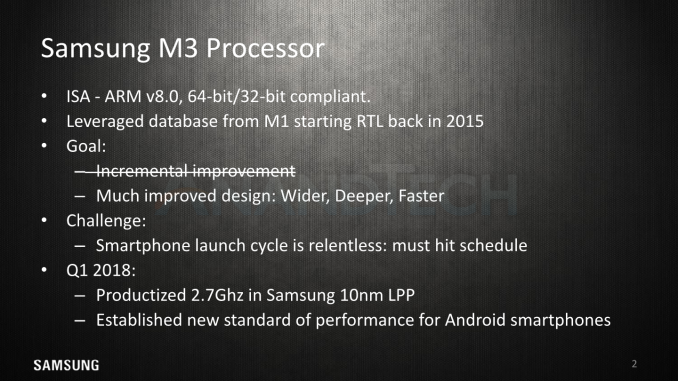
The Exynos M1 being designed from scratch, it’s natural to expect that follow-up generations would be using it as the starting point for further development. Following the tape-out of the M1, the SARC team started off the M3 design with the existing M1 RTL back in Q1 of 2015. At first, this was meant to be an incremental development. However, there was a larger change of plans later on in Q1 2016, as goals were set higher for a much larger performance push.
The existing improvements were forked in Q3 2015 into what became the M2 – which was initially meant to only be a 10LPE port of the M1 (Which was 14LPP). As a reminder, the M2 had a robust ~20% IPC improvement across workloads, which allowed it to outperform the M1 even though it was clocked 12% slower in production silicon. Samsung had achieved this by implementing some of the originally planned M3 features into the M2, while the new M3 design became more aggressive.
Here Samsung clearly states one of the industry’s most unforgiving aspects: a relentless launch cycle in which the IP and silicon must be in sync with. Many issues that we’ve seen in SoCs from various vendors, both in terms of performance and especially in terms of power consumption are mostly due to the fact that there was a rush to market in order to catch the commercial release window for new products.
Samsung's Exynos M3 - Introducing Meerkat
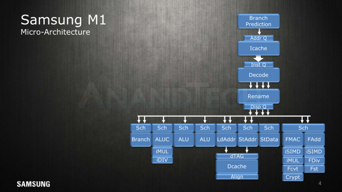
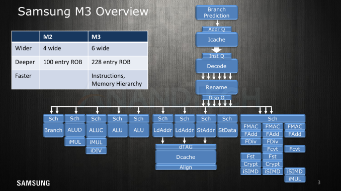
Starting off with a high-level overview of the Exynos M3 alongside with the original slide of the M1, we see big similarities, yet the M3 just adds more onto the table. The SARC team increased the microarchitecture width from a 4-wide decode unit to a 6-wide, the overall core defining characteristic of the new µarch. We see an added integer ALU with multiplier capability, a second load unit and a vastly expanded floating point / SIMD complex with up to triple the compute capacity.
We never really had a microarchitecture disclosure of the M2 and there’s also no specific compiler machine model tied to it, but among one of the changes revealed today is that the reorder buffer has seen a minor adjustment from 96 to 100 entries. As mentioned in our first µarch disclosure back in January, the M3 vastly expands this to up to 228 entries, making this aspect of the µarch a lot more similar to the what we see in Intel’s core designs - although we can’t make a direct density comparison across different ISAs as instruction complexity varies.
When Arm disclosed the A76 µarch details and particularly the 128-entry ROB (which in comparison seems quite small to the M3), they said that this was a balance between performance and area/power. In particular we saw a mention that a 7% increase in the ROB capacity only came with a 1% performance gain on average.
Samsung explains that ROB capacity is a choice which is tied to the design of the rest of the microarchitecture and the various buffers and backend scheduler capacities – µarch depth and µarch width are complementary to each other for performance. A wider µarch such as the M3 is able to fill the ROB faster and thus get more performance return out of the larger capacity. Overall the M3 is said to have been made with a different set of decisions than the M1/M2, aiming for the higher performance while taking into account the associated costs.
A Much Larger Front-End
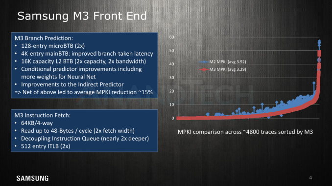
Diving into more details on the front-end, we see the various improvements on the branch predictor and fetch units. The M1’s branch predictor differed from other µarch’s in that it was able to take two branches per cycle and having two branch ports on the backend. The M3 seems to maintain this width, but doubles up the µBTB from 64 to 128 entries. The mainBTB remains at 4K entries but has had latencies improved for taken branches.
On top of this the branch predictor quality overall has been increased – resulting in a 15% average reduction in missed branches. It was interesting to see Samsung actually publish an actual MPKI (Misses per kilo instructions) value here as it's something we haven’t seen acknowledged by Arm (or any vendor?) to date. Here Samsung monitors a continuously expanding suite of 4000-6000 code traces from various applications and use-cases against which it validates its performance against during development.
The branch predictor and fetch units respectively feed a decoupled address queue and a decoupled instruction queue, this is likely done so that the units can be clock gated in the implementation.
The fetch unit’s bandwidth has been doubled and now can read up to 48 bytes per cycle which corresponds to 12 32b instructions per cycle – this results in a 2:1 ratio of fetch versus decode capacity which is an increase over the 1.5:1 ratio (24B/c, 4 decode) in the M1. Samsung explains that the big increase is needed to combat the increasingly big problem of branch bubbles on wider microarchitectures. They admit that on average, the distance between taken branches is less than 12 instructions, but the larger width helps a lot for temporary bursts of instructions.
While this change has a high instantaneous power utilisation, when the instruction queue (which is now double the depth) gets filled faster than the decode unit can drain it, it has an overall net positive effect on power used as it allows the fetch unit to be clock gated. Here the overall energy efficiency is more tied to the branch predictor quality as it doesn’t actually matter when an instruction is fetched, only with a larger “batch” such as implemented here, there might be more overhead in the thrown away instructions in case of a wrongly taken branch path.
The instruction cache / L1I comes at 64KB. We’re not sure if this is an increase over the M2 as it’s hard to measure, but it definitely is double the size of the M1 µarch.
The instruction translation lookaside buffer (ITLB) has grown from 256 to 512 entries. It’s to be noted here that Samsung is employing a three-level hierarchy as opposed to what we see in Arm’s processors. The A75 and A76 respectively have a first-level 32 and 48-entry µITLB, with a clustered mainTLB of a total of 1280 entries, consisting of 1024 entries for pages up to 64KB and a secondary 256-entry table for pages >=1MB.
Samsung has a first level data and instruction TLB as well, but doesn’t disclose the size of the L1 ITLB. The last level unified TLB for Samsung is also larger at 4096 entries, we’ll come back to it on a later slide.
The Middle-Machine: Wider Decode, Rename, & Dispatch
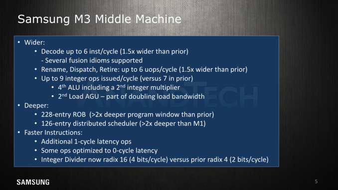
Moving onto the middle machine (decoder, rename, dispatch), we come back to the fact that we see a 1.5x wider decode unit. Samsung isn’t disclosing any details here, but it has improved the instruction/µOP fusion capabilities. Rename and dispatch throughput match the decode width; here it’s important to not try to read too much into it and compare it to Arm’s CPU cores as we’re talking about different µOP types between the vendors. Here Samsung µarch has supported forms of multi-dispatch since the M1; the decoder emits a µOP which can dispatched to multiple schedulers simultaneously, but it still only counts it as one dispatch and one entry in the ROB.
In the integer core we see two additional schedulers, so the M3 is now able to issue 9 µOps over the 7 in the prior generations. One of the new ports is an additional ALU unit with multiplication capability, doubling the MUL throughput and increasing the simple integer arithmetic throughput by 25%.
The secondary additional port is a second load AGU which enables doubling of the load bandwidth of the core.
A "Beast" of a Floating Point Unit
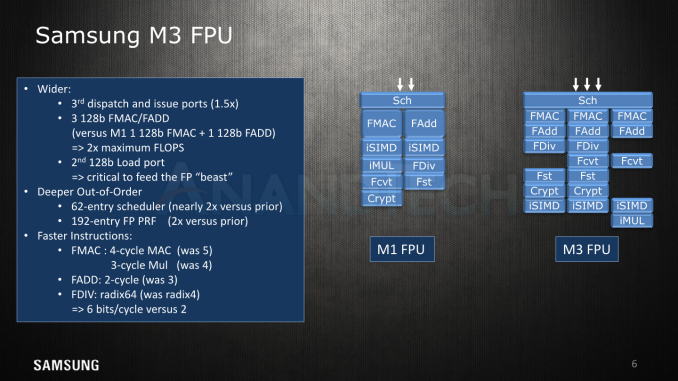
In the floating point core, we see a very different “beast” compared to the prior µarch. Here Samsung added a third pipeline, increasing the µOPs dispatched into and issued in the FPU. In terms of simple floating point capability, the M3 triples the multiply and arithmetic throughput by having 3 128b FMAC/FADD units over the M1’s single FMAC+FADD unit. In terms of FLOPS this represents a doubling of maximum throughput from 3 FLOPS (1x FMAC (2) + 1x FADD (1)) to 6 FLOPS (3x FMAC (2)).
Naturally because the execution throughput has increased so drastically it was necessary to scale up the scheduler and physical register files, doubling both of them from 32 to 62 for the schedulers and 96 to 192 entries for the FP PRFs.
Samsung has worked hard to reduce the execution latencies, and this also applies to the floating point pipelines. Here the multiplication unit has shaved off a cycle from 4 to 3 cycles also benefitting FMAC operations, going down from 5 to 4 cycles. Simple floating point addition shaved off a cycle from 3 to 2, as well as the FDIV seeing an upgrade to a Radix-64 unit significantly reducing division latencies.
Going on a little tangent here, I remember Arm had hyped its new floating point pipelines in the A76 for several years now, and they were very proud in the “state-of-the-art” VX datapaths of the new core. Well, at least from the higher level specifications it seems that Samsung beat Arm to the punch by a year as the M3 features equivalent floating point latencies while having higher execution throughput as well as even lower latency ASIMD capabilities. Obviously we’ll get to compare these in more detail in the future when we can test the silicon side-by-side.
New Load/Store Unit For Feeding It Data
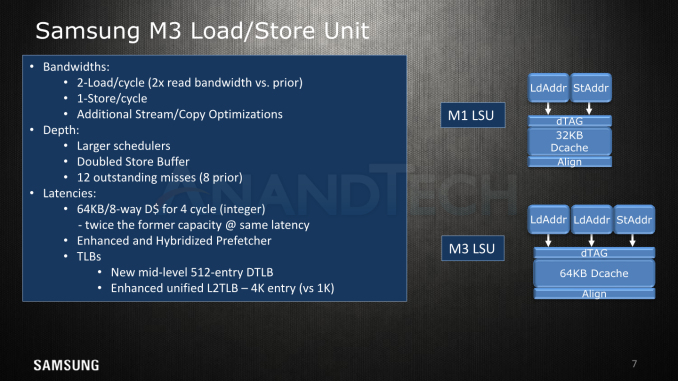
In the load/store unit we again see the doubling of the read bandwidth thanks to the addition of a second 128b load port. Here the load-use latency remains the same at 4-cycles. Store bandwidth is the same at 1 store per cycle with a 1-cycle latency. Again the M3 for this generation has a double bandwidth advantage as its two LD units operate at 128b/cycle versus 64b/cycle for the A75; the A76 will even this out next generation.
Overall the LD/ST scheduler’s capacities have been increased, and we see a doubling of the store buffer, although we don’t have exact values. To better serve the wider µarch, the outstanding misses on the L1 data cache has been increased from 8 to 12, meaning the unit can serve up to 12 concurrent data requests during cache misses while the core/system fetches the data from the higher-hierarchy cache levels or memory. This seems maybe low given the machine width of the M3 µarch – Arm hadn’t publicly disclosed the specifications for the A75 and prior in this regard but they made a MLP/memory level parallelism a big focus-point of the A76 disclosure, here the L1D services up to 20 outstanding misses which is more than the M3 can do, even though it’s a narrower machine.
Here Samsung’s prefetchers would need to be of top quality to avoid any memory bottlenecks and achieve the goal of an optimal perfect cache-hit operation, and indeed they say that there’s been enhancements into the new “hybridized” prefetchers. Here hybridized essentially means there’s going to be more prefetchers, or a single prefetchers able to deal with different kind of memory patterns.
The slides again mentioned the new TLB hierarchy we described earlier on the instruction side. Here on the data side we see the same 32-entry micro-DTLB as on the M1, however there’s now a new mid-level DTLB with 512 entries. Both the instruction TLBs and data TLBs are now serviced by an enhanced and larger unified L2 TLB with 4096 entries versus the 1024 entries in the prior generation.
Core Pipeline: Everything Has A Cost
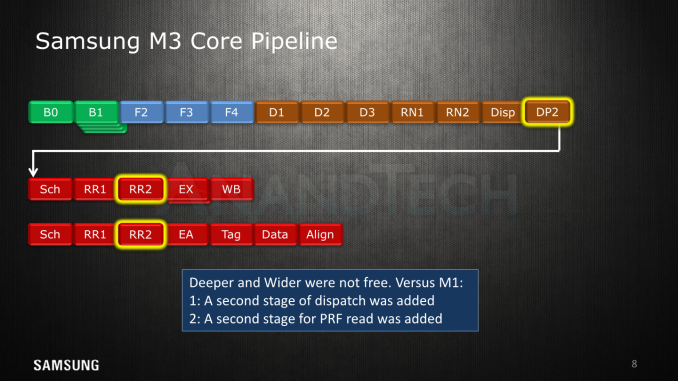
Naturally widening the microarchitecture comes at a cost, and the M3 adds two cycles to its pipeline depth when compared to the Exynos M1. A secondary dispatch stage was added, as well as a second stage for register read. Usually CPU pipeline depth is counted as the stages from predict/branch to register write-back, and in this case the M3 is quite deep at 17 stages, versus 15 stages for the M1 and 13 stages for the A75 and A76.
Branch misprediction penalty is 16 cycles as there’s a drive cycle back to the frontend, again 2 cycles more than the 14c penalty on the M1. Samsung didn’t say if the µarch had any kind of other fast-paths between the stages to reduce latencies in critical cases. The M3, and partly the M1’s disadvantages over its Arm counterpart are located in the 3 vs 2-stages fetch and decode units (+2 stages), a 2 vs 1-stage register rename unit (+1), and the need for a second dispatch stage (+1).
Samsung admits that while this is a negative, it was a necessary evil in order to get the bigger µarch done on schedule, and while the machine does well with branch mispredicts, it is a cost for the new µarch.
In general it’s odd to see that Samsung’s deeper microarchitecture choices haven’t actually resulted in much of a clock speed advantage in actual products. Here it seems that the competition might be doing a better job in the physical design and the limiting critical paths in order to achieve higher frequencies at reasonable voltages.
A New 3-Level Cache Hierarchy
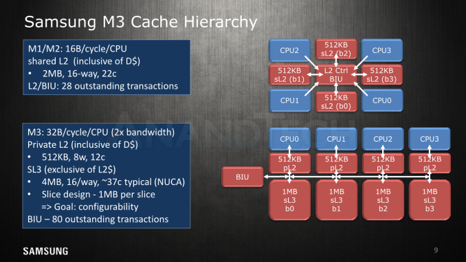
Moving away from the CPU core itself, we’re having a look at the new L2/L3 cache hierarchy. Like the A75 and A76, the M3 introduced a new private L2 cache as an intermediate level between the core and the shared last-level cache. The new private L2 is inclusive of the lower data caches and comes at 512KB per core. The access latency versus the shared L2 in the M1 was reduced from 22 cycles down to 12 cycles. Here it seems that Samsung would be at a disadvantage to Arm’s A75 as the latter discloses a L2 hit latency of only 8 cycles. It’s to be noted that in actual physically implemented silicon this figure might go up due to design choices in the RAMs and physical layout. In practice the Snapdragon 845’s L2 latencies at 2.8GHz measure in at ~4.4ns versus ~4.6ns for a 2.7GHz Exynos 9810 in our measurements.
Bandwidth to the L2 cache has also been doubled, now achieving 32B/cycle versus 16B/cycle for the M1. The A75 for comparison reads 16B/cycle from the L2 while writing into it at 32B/cycle.
At first there was a bit of a confusion when the Exynos 9810 was announced as to how its L3 cache works. Eventually we got clarification that Arm doesn’t actually allow third-party cores to plug into its DynamiQ cluster/L3 system, and the die shot of the new SoC finally undoubtedly confirmed that the new silicon has nothing to do with Arm’s counterpart.
Here we see a large 4MB cache implemented in a NUCA (Non-uniform cache architecture) fashion with four slices of 1MB, with each slice being located opposite of a CPU core. Because of the non-uniform layout, the access latencies between the cores and the slices are not the same. A core accessing an adjacent slice has latencies of 32 cycles, while the furthest distance between a CPU and slice has latencies of 44 cycles. Samsung quotes an average latency of 37 cycles in typical patterns.
It’s here where the M3 seems to be weaker compared to Arm’s implementation. Arm quoted L3 hit latencies of 25 cycles for an A75. In practice again we see the Snapdragon 845 achieving ~9.4ns while the Exynos 9810 starts at ~11ns nearest to the depth size of the L2 cache and goes up to ~20ns reaching the 4MB test depth of the L3. Here the fact that that Samsung’s L3 implementation is meant to be run at higher frequencies (2.7GHz in the above values) and is on the same clock plane as the CPUs doesn’t help it as the cycle access latency disadvantage is too great, even in the face of the lower clocked 1478MHz DSU of the Snapdragon 845. While the DSU’s lower maximum clock can be a disadvantage, it is actually very much an advantage in the opposite scenario; when the CPU cores are clocked lower, they could still take advantage of a fast running DSU/L3 cache and its lower latencies. The M3’s cache hierarchy in contrast slows down along with its CPU cores.
The M1/M2’s bus unit handled up to 28 outstanding misses while the M3’s handles up to 80 outstanding misses – there’s a lack clarity here on if this applies to the L3 or if somehow the L2 blocks are included in this figure. Arm never talked about the A75’s capabilities here but details that the A76 is be able to handle 46 outstanding misses on the L2 caches with 94 outstanding misses on the DSU’s L3.
Data partitioning between the L3 slices is decided by address hash, and all slices are powered on at the same time. In contrast, a DSU in a larger SoC is by default implemented with two slices, of each which can be half powered down – giving a granularity of ¼ of the L3 in terms of power-down capability. I’m not sure how the SD845 is implemented here as it’s difficult to determine it on a lower-resolution die shot.
Finally Samsung explains this slice design is meant to achieve better configurability for different designs beyond premium mobile, which of course is still the highest priority. Samsung is likely pointing at either large form-factor designs or what I may think is more likely, S.LSI’s efforts in the automotive space.
Overall for the cache hierarchy Samsung admits that the end product didn’t quite achieve what they really wanted. The end-product ended up like this because of necessary trade-off to make in order to get the 3-level cache hierarchy implemented for this generation. Here I think we’ll a much larger focus for the next generation M4.
Physical Layout: Making Sense of the Silicon Blocks
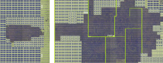
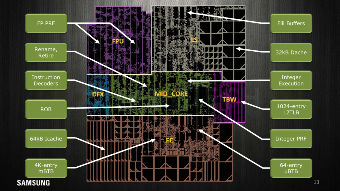 Exynos M1 Core Layout
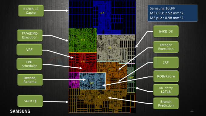
Exynos M3 Core Layout
Samsung delights us with this disclosure this year, as they break down the core’s floor plan in this slide. I’m pretty happy to have been almost accurate with the medium resolution die shot I had at hand in delimiting the various function blocks in the original review article.
Here’s some short explanations on the terms:
- pL2: Private L2 cache, here we see the 512KB cache implemented in what seems to be two banks/slices.
- FPB: Floating point data path; the FP and ASIMD execution units themselves.
- FRS: Floating point schedulers as well as the FP/vector physical register file memories.
- MC: Mid-core, the decoders and rename units.
- DFX: This is debug/test logic and stands for “design for X” such as DFD (Design for debug), DFT (Design for test), DFM (Design for manufacturability), and other miscellaneous logic.
- LS: Load/store unit along with the 64KB of L1 data cache memories.
- IXU: Integer execution unit; contains the execution units, schedulers and integer physical register file memories.
- TBW: Transparent buffer writes, includes the TLB structures.
- FE: The front-end including branch predictors, fetch units and the 64KB L1 instruction cache memories.
Exynos 9810 Floor Plan. Image Credit TechInsights
Overall compared to the M1, almost all facets of the functional units in the M3 have vastly increased in size. The end product ends up at 2.52mm² for the core’s functional blocks, plus another 0.98mm² for the 512LB L2 cache and logic.
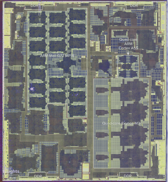
Exynos 9810 Floor Plan. Image Credit TechInsights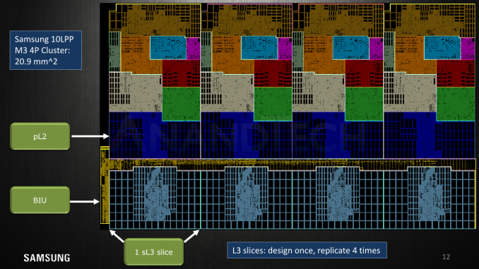
Here Samsung showcases the whole cluster floorplan, again marking the 4 cores laid down next to each other in a row with the L2 and L3 slides also orderly placed next to each other. This layout seems to have saved some layout efforts as each block is designed once and then simply replicated 4 times.
59% Higher IPC Across Variety of Workloads
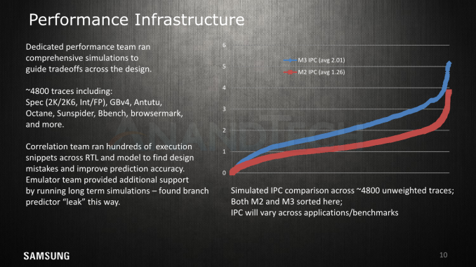
Finally Samsung talks a bit about their performance profiling infrastructure and how they run various amounts of workload traces through the RTL and model simulators in order to evaluate design choices, find mistakes, and do fine-tuning to the µarch.
In this slide we finally have an official figure for the IPC increase for the core: ~59%. I had pointed out at >50% at the beginning of the year, so I'm glad to see that work out in the end. As we see in the graph, the increase is naturally not linear across all workloads and we see limited increases of only 25% in high ILP workloads, to near to not much of an increase in what is likely to be MLP workloads. Conversely, there’s also a lot of mixed workloads where the IPC increase is >80%.
Performance & Efficiency: Samsung's Data and AnandTech's Data
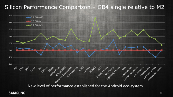
The next slides showcase a snippet of the performance improvements on GeekBench4 between the M2, M3, and the A75; representing commercial performance on the Exynos 8895, Exynos 9810 and the Snapdragon 845.
Again we’ve already very much extensively covered the performance aspects of the SoC and microarchitecture in past articles;
- The Samsung Galaxy S9 and S9+ Review: Exynos and Snapdragon at 960fps
- Improving The Exynos 9810 Galaxy S9: Part 1
- Improving The Exynos 9810 Galaxy S9: Part 2 - Catching Up With The Snapdragon
To add to today’s µarchitecture article I’m also adding some new SPEC scores which improve on the originally review data. The difference and cause for the improvement is DVFS tweaking, further scheduler enhancements, and a more synthetic testing environment and care with coping with the higher power draw at the M3’s maximum frequencies.
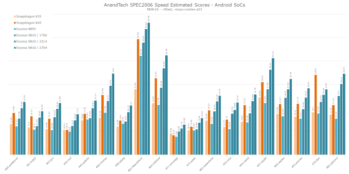
Click for large full resolution
I won’t go over the details of the scores, but the performance improvements under the new conditions more closely represents the kind of high jump Samsung showcases in GB4.
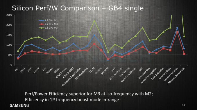
Power efficiency has been a big topic for the M3 – and here it is quite telling that they chose to omit results of competing solutions. As we’ve covered in our reviews, Samsung’s high boost clock at up to 2.7GHz comes at a price of very high required voltages and exponential power draw. Here, even though it showcases leading edge performance, it ends up less efficient than the Exynos 8895’s M2. The figures here represent active system power; that means CPU, memory controller, DRAM, much in the same way we measure it here at AT.
Reducing the clock to the same 2.3GHz as the M2, we see the M3 lead in terms of efficiency as per Samsung’s presentation.
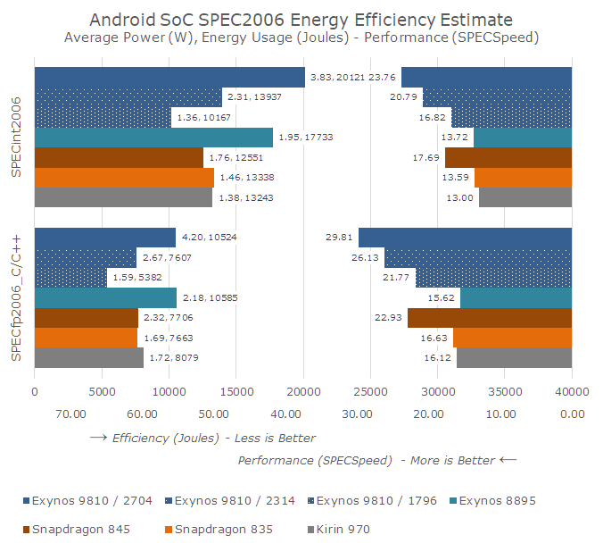
To add to Samsung's data and give more context, I’m reposting the revised benchmark and efficiency overview in our own independently performed analysis of the platform. The below chart showcases the energy usages to finish the workload suite, alongside the average power consumption during the test. The left bars represent the consumed energy in Joures, and the shorter the bars are (the less energy), the more efficient a platform is. The right bars represent the performance score, the longer the bars denoting better performance.
I’ve also re-tested the workloads at the three top-frequencies of the M3; 1794, 2314 and 2704MHz, giving us a wider idea of how the efficiency scales with performance.
Overall the M3 offers a quite dynamic range in its results. At (almost) equivalent peak performance against the competing A75 results for this generation, the M3 is able to post a good efficiency advantage. This lower performance point of the M3 still outperforms the 2.3GHz maximum performance of the M2 – all while having significant power and energy efficiency advantages.
Clocking it up to 2.3GHz here the M3 more clearly outperforms the A75, albeit at an efficiency hit in the integer workloads, while the FP workloads closely match the Arm competition.
Finally the 2.7GHz results further the performance gap, but comes at a great cost in efficiency, using up more energy than any other recent SoC.
The fact that the E9810 had a cluster of 4 M3 cores running on the same frequency and voltage plane came at a cost of overall efficiency. Secondary threads that didn’t require the peak performance driven by a larger primary thread, but whose requirements are still bigger than the capacity of the littles cores, had to take a large the efficiency hit of running at the same bad efficiency points as the biggest thread in the cluster. The result of this adds to the bad battery life scores we’ve come to measure.
I’ve been able to resolve the scheduling issues in a custom kernel, improving the web browsing score further to 9h, however there are still compromises that just can’t be resolved due to how the SoC operates. Here I expect Samsung to depart from the 4 “huge core” topology for the next generation M4 and introduce something that will be a lot more power efficient in diverse multi-threaded scenarios.
Samsung's Future Strategy & Conclusion
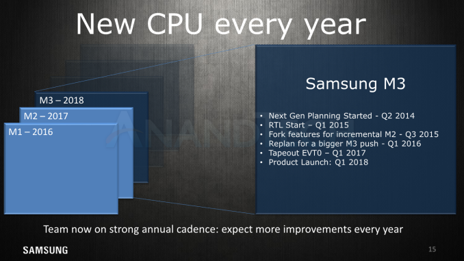
Lastly, Samsung talks more about the project’s timelines and how things got put into motion. As we discussed in the introduction, the M3’s planning was kicked off in 2Q14 with RTL start in 1Q15, following the completion of the M1. During this time, Samsung had a change of cadence and planning, forking a subset of features originally planned for the M3 and putting them in into the M2 in 3Q15. Here the original M3’s plans were revised for a bigger microarchitecture push for performance in the first quarter of 2016.
The RTL was handed off to the SoC team in 1Q2017 for the first EVT0 tapeout of the Exynos 9810. It’s to be noted that actual production silicon is EVT1, whose tape-out happened sometime in the middle of 2017. Finally the Exynos 9810 saw commercial availability in March 2018.
The M3 is said to have been quite a sweat-breaking effort for the design team, having to have gone through what seems to have been a major replanning of the project, and having to deal with extreme time-pressure in terms of hitting a hard deadline in order to make it into the next generation product.
Here it seems Samsung still left a lot of improvements on the table that didn’t make it into the M3 due to time constraints. The cache hierarchy in particular what seems to be one of the weaker parts of the microarchitecture, which is something Samsung admits they aren’t quite happy with. It was one of the features that pushed the design team hard in order to make out the door in time.
One aspect that Samsung didn’t, and wasn’t willing to talk about, is any kind of physical implementation details. As HotChips is a microarchitecture forum, the disclosures were kept to the µarch of the M3. As we’ve seen in the past, a single microarchitecture can end up quite differently in its performance and power characteristics when implemented differently by vendors. Taking this into account, when measuring the end-product, it’s hard to separate these intertwined aspects of a piece of silicon.
The M3 seems like an overall solid microarchitecture which feels a lot more like what we see in desktop grade products. It also feels like Samsung took a more straightforward approach in terms of leveraging performance out of the µarch – in many aspects it’s just a much bigger beast than what we see from Arm – and thus also explains the M3’s quite large silicon size.
When evaluating efficiency of a piece of IP, looking at the higher-level microarchitecture is not enough, and here aspects of the actual electrical engineering of the transistor structures and details in their design choices can easily outweigh any apparent higher level characteristics. Here we’re largely out of our depth and no vendors will really ever make disclosures of such detail, not to mention it would be vastly out of scope for public readerships.
Here the final slide contains probably the most revealing disclosure that gives us a glimpse of Samsung’s future strategy: the SARC design team is said to now be on a strong annual release cadence with continued improvements every year. Indeed when I was making comparisons between the M3 and A76 in asking about some different design choices and specifications, Samsung didn’t shy in reminding me that the real competition for Arm’s new core will be next year’s new Exynos M4, not the M3.
We’ve only had two generational improvements released to date, but with 20% and 59% in IPC gains for the M2 and M3, Samsung does post an albeit short, but very robust track-record. Only just days ago Arm publicly announced its performance core roadmap through to 2020, revealing A76 successors Deimos and Hercules, promising ~15% and 10% generational gains. Here the M3 already seems to match or exceed the A76 in projected performance (at least in SPEC2006), so depending on the power efficiency of the M4, we might finally see a competitive advantage pay-off for Samsung’s custom designs.
Overall, we do thank Samsung for doing microarchitectural disclosures such as seen today, as beyond Arm’s own products, they are a quite a rare event in the ever so secretive industry. Here’s to hoping S.LSI and SARC resolve the Exynos 9810 and M3’s weaknesses and are pushing hard to make next year’s SoC a larger success. We’ll definitely looking forward to get our hands on it!

