Original Link: https://www.anandtech.com/show/13075/intel-acquires-easic-lower-cost-asics-in-fpga-design-time
Intel To Acquire eASIC: Lower Cost ASICs in FPGA Design Time
by Ian Cutress on July 12, 2018 3:00 PM EST
Along with the other announcement today, Intel is also announcing that it will acquire a company called eASIC which develops FPGA-like design tools to roll out ‘structured ASICs’. These structured ASICs an intermediary between a full FPGA and a full ASIC that allow for a quick roll out time and cheaper production cost. Technically Intel has been using eASIC technology since at least 2015 in its custom Xeons, however today’s announcement means that the eASIC team will become part of Intel’s Programmable Solutions Group (PSG). The deal is expected to close within the next month.
For everyone used to mentioning CPUs and GPUs when it comes to computer technology, there are other classes of processor units to be aware of. FPGAs, or Field Programmable Gate Arrays, such as those from Altera or Xilinx, use several million Logic Cells in a chip that can be configured to represent any portion of a semiconductor processor design. In fact most CPUs and GPUs are simulated on FPGAs first, before being manufacturered, to ensure that they work. FPGAs offer a quick way to design a circuit in a circuit, and the FPGA market is big business. FPGAs can also contain ‘hard’ logic blocks, such as ARM cores or transceiver modules for off-chip communication.
The other side of the equation is an ASIC, or Application Specific Integrated Circuit, is a chip designed for only a fixed number of purposes. Often ASIC designs are highly optimized, with no excess die area for additional logic. Often a CPU and a GPU are considered ASICs, in the sense that their microarchitecture is fixed, but the calculations in CPUs/GPUs have conditions and branches: for ASICs, the data and operation is known, and the circuit is designed to take that into account. ASICs are to a large extent non-configurable, but very fast and very low power, but can be expensive to build on the leading processes. Some companies with low volume ASICs sometimes deploy their designs on FPGAs to customers, because of time, cost, and scale, at the expense of power.
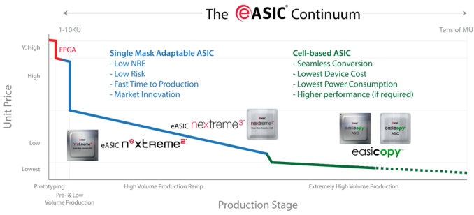
What the eASIC ‘structured ASIC’ does is more of a half-way house. Engineers can create a design using an FPGA, then rather than spending time optimizing the circuit layout, they bake the fixed layout into a single design mask for manufacturing. By being a fixed design like an ASIC, it is faster than a variable design, but without the die area benefits of ASIC-like power savings. However, it was designed in FPGA time, rather than ASIC time (up to six months saved), and saves power through its fixed design. The eASIC add-in is that it uses a single mask layer customization to replace SRAM based routing with a scheme that uses via, reducing the cost significantly at the point of manufacture. eASIC also provides hard-coded cell libraries within its single layer, further reducing power, die area, and time to market. Designers can also forgo standard ASIC tasks such as clock balancing, signal integrity analysis, power droop, and test insertion. The structured ASIC is ultimately no longer programmable, and if you took saws to inside a chip then it will look like an FPGA, but ultimately it has some benefits over a pure ASIC by having the time to develop benefits of an FPGA with extra power reductions.
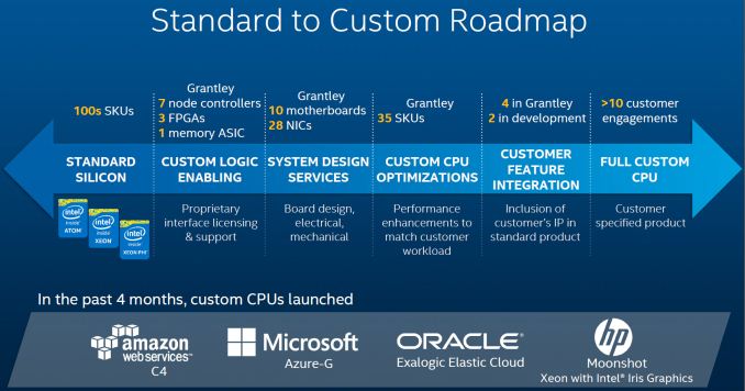
As mentioned, Intel have already been working with eASIC since at least 2015 for its custom Xeons, as referenced in this news post back in 2015. Intel stated back then that it was looking to eASIC’s technology to allow its customers to integrate reprogrammable technology within a Xeon package to improve workflow, performance, power, and cost. Aside from the standard Xeon processors that Intel normally ships publically, Intel works with major customers to create custom CPU designs, as referenced in this older slide:
As shown in the ‘custom CPU optimizations’ and ‘customer feature integration’, Intel purposefully adds features to its Xeons, some of which are made public, to help assist with workflow. With the latest generation of Xeon Scalable processors, this can also be extended to extra chips on-package built through eASIC designs. However, now that Intel is acquiring the technology and moving it in house, Intel will have a better vertical integration of this technology, as well as having the ability to expand it to other product areas.
Currently eASICs newest product lines are built on GlobalFoundries 28nm, and TSMC for older products. When the deal closes, Intel is expecting to look deep into the projected roadmap and decide if transitioning onto Intel processes quickly will be feasible. Intel stated that maintaining business continuity will be expected, and the picture will become clearer after the deal has closed.
As a result of this acquisition, Intel gains the eASIC assets and team, which is around 120 people. The company was originally based in Santa Clara, and over time the group may movedown the road to be closer to the resources in Intel’s Programmable Solutions Group. Details of the acquisition were not disclosed.


