Original Link: https://www.anandtech.com/show/12910/amd-demos-7nm-vega-radeon-instinct-shipping-2018
AMD Demos 7nm Vega GPU: Betting Big on Machine Learning for Radeon Instinct; Shipping This Year
by Anton Shilov on June 6, 2018 1:30 AM EST- Posted in
- AMD
- Radeon
- GPUs
- Vega
- 7nm
- AMD Instinct
- AI
- Computex 2018
- 7LPP
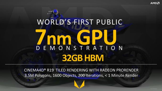
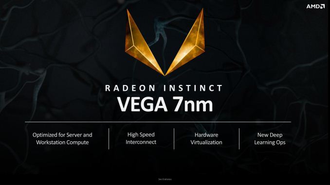
In a fairly unexpected move, AMD formally demonstrated at Computex its previously-roadmapped 7nm-built Vega GPU. As per AMD's roadmaps on the subject, the chip will be used for AMD’s Radeon Instinct series accelerators for AI, ML, and similar applications.
The 7nm Vega GPU relies on the 5th Generation GCN architecture and in many ways resembles the Vega 10 GPU launched last year. Meanwhile, the new processor features a number of important hardware enhancements, particularly deep-learning ops specifically for the AI/ML markets. AMD isn't detailing these operations at this point, though at a minimum I'd expect to see Int8 dot products on top of Vega's native high speed FP16 support.
AMD also briefly discussed the use of Infinity Fabric with the new 7nm GPU. AMD already uses the fabric internally on Vega 10, and based on some very limited comments it looks like they are going to use it externally on the 7nm GPU. On AMD's Zeppelin CPU dies - used in the EPYC CPU lineup - AMD can switch between Infinity Fabric and PCIe over the same lanes depending on how a product is configured, so it's possible we're going to see something similar here. In other words, AMD can kick in Infinity Fabric when they have something else to connect it to on the other end.
As a part of its demonstration, AMD also disclosed that the prototype Radeon Vega Instinct accelerator card carried 32 GB of HBM2 memory spread across four KGSD stacks. Assuming that these are 1024-bit HBM2 stacks, it looks like the new Vega got a 4096-bit bus, which will be welcome with the HPC crowd.
Otherwise, AMD is not disclosing the exact specifications of the 7nm Vega GPU, so we don't know how many CUs and other functional blocks the chip has. Compared to GloFo's 14nm process, the density savings of 7nm are significant. However I fully expect AMD to immediately reinvest those savings into more CUs, more memory controllers, etc.
Though based on some very rough paper napkin math coming the size of the HBM2 packages to the GPU die, a really conservative estimate for the die size puts it around 14mm X 24mm, or 336mm2. Though this is quite likely an underestimate, and we'll redo our calculations if we can get some better photos of the chip.
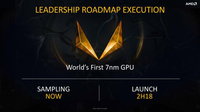
One especially bright spot for AMD here is that their shipping schedule has moved up by at least a quarter. Previously AMD was going to have the 7nm GPU sampling by the end of the year and shipping in 2019. Instead the 7nm Vega GPU is sampling now and the launch window has been moved up to H2'18. This is an incredibly aggressive schedule, given that we're only expecting the first 7nm SoCs - decidedly smaller devices that make for good pipecleaners - to ship in the same timeframe. So AMD appears to be taking the NVIDIA route and shipping their big GPU early, eating any yield issues in the process. It's a risky strategy, but if customer demand is there, then as we've seen in NVIDIA's case, it can pay off handsomely.
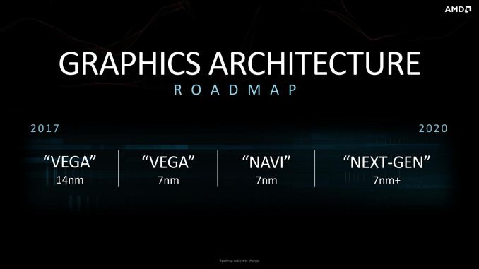
Finally, Lisa Su also quickly reiterated that the rest of AMD's GPU roadmap hasn't changed from earlier this year. This means that after the 7nm Vega GPU for compute users, AMD will be bringing 7nm GPUs out to gamers & other consumers as well in the form of Navi. AMD has not announced a timeframe for this, but we're certainly not expecting this until sometime in 2019.

