Original Link: https://www.anandtech.com/show/12195/hisilicon-kirin-970-power-performance-overview
HiSilicon Kirin 970 - Android SoC Power & Performance Overview
by Andrei Frumusanu on January 22, 2018 9:15 AM EST
Today I would say that there’s only two truly vertically integrated mobile OEMs who have full control over their silicon: Apple and Huawei – and of the two one could say Huawei is currently even more integrated due to in-house modem development. Huawei’s semiconductor division, HiSilicon, has over the last several years been the one company which seems to have managed what the others haven’t: break in into the high-end market with solutions that are competitive with the current leader in the business, Qualcomm.
I remember the Honor 6 with the newly branded (Previously not having any “halo” line-up name) Kirin 920 SoC as the first device with the company’s in-house SoC that we reviewed. These and the following generation the Kirin 930 suffered from immaturity with problems such as a very power hungry memory controller and very disappointing camera processing pipeline (ISP/DSP). The Kirin 950 was in my opinion a turning point for HiSilicon as the product truly impressed and improved the quality of the product, catching many eyes in the semiconductor industry, including myself in the resulting review of the Huawei Mate 8.
Over the last several years we’ve seen great amounts of consolidation in the mobile semiconductor industry. Companies such as Texas Instruments which were once key players no longer offer mobile SoC products in their catalogue. We’ve seen companies such as Nvidia try and repeatedly fail at carving out meaningful market-share. MediaTek has tried providing higher end SoCs with the Helio X line-up with rather little success to the point that the company has put on hold development in that segment to rather focus on higher margin parts in the P-series.
Meanwhile even Samsung LSI, while having a relatively good product with its flagship Exynos series, still has not managed to win over the trust of the conglomorate's own mobile division. Rather than using Exynos as an exclusive keystone component of the Galaxy series, Samsing has instead been dual-sourcing it along with Qualcomm’s Snapdragon SoCs. It’s therefore not hard to make the claim that producing competitive high-end SoCs and semiconductor components is a really hard business.
Last year’s Kirin 960 was a bit of a mixed bag: the SoC still delivered good improvements over the Kirin 950 however it was limited in terms of what it could achieve against competing flagship SoCs from Samsung and Qualcomm as they both had a process node advantage. Huawei's introduction of flagships with new generation of SoCs in the fourth quarter is more close to the release time-frame of Apple than the usual first quarter that we’ve come accustomed of Qualcomm and Samsung.
As such when pitting the Kirin versus Snapdragon and Exynos’s we’re looking at a product that’s more often than not late to the party in terms of introduction of new technologies such as process node and IP. The Kirin 970 fits this profile: as a 10nm Cortex-A73 generation-based SoC, it lagged behind Qualcomm and Samsung in terms of process node, yet being too early in its release to match up with ARM’s release schedule to be able to adopt DynamiQ and A75 and A55 based CPU cores for this cycle. That being said the Kirin 970 enjoys a few months with technical feature parity with the Snapdragon 835 and Exynos 8895 before we see new Snapdragon 845 and Exynos 9810 products later in the usual spring refresh cycle.
Nevertheless, the article today is a focus on the Kirin 970 and its improvements and also an opportunity to review the current state of SoCs powering Android devices.
| HiSilicon High-End Kirin SoC Lineup | |||
| SoC | Kirin 970 | Kirin 960 | Kirin 950/955 |
| CPU | 4x A73 @ 2.36 GHz 4x A53 @ 1.84 GHz |
4x A73 @ 2.36GHz 4x A53 @ 1.84GHz |
4x A72 @ 2.30/2.52GHz 4x A53 @ 1.81GHz |
| GPU | ARM Mali-G72MP12 746 MHz |
ARM Mali-G71MP8 1037MHz |
ARM Mali-T880MP4 900MHz |
| LPDDR4 Memory |
4x 16-bit CH LPDDR4 @ 1833 MHz 29.9GB/s |
4x 16-bit CH LPDDR4 @ 1866MHz 29.9GB/s |
2x 32-bit LPDDR4 @ 1333MHz 21.3GB/s |
| Interconnect | ARM CCI | ARM CCI-550 | ARM CCI-400 |
| Storage I/F | UFS 2.1 | UFS 2.1 | eMMC 5.0 |
| ISP/Camera | Dual 14-bit ISP | Dual 14-bit ISP (Improved) |
Dual 14-bit ISP 940MP/s |
| Encode/Decode | 2160p60 Decode 2160p30 Encode |
2160p30 HEVC & H.264 Decode & Encode 2160p60 HEVC Decode |
1080p H.264 Decode & Encode 2160p30 HEVC Decode |
| Integrated Modem | Kirin 970 Integrated LTE (Category 18/13) DL = 1200 Mbps 5x20MHz CA, 256-QAM UL = 150 Mbps 2x20MHz CA, 64-QAM |
Kirin 960 Integrated LTE (Category 12/13) DL = 600Mbps 4x20MHz CA, 64-QAM UL = 150Mbps 2x20MHz CA, 64-QAM |
Balong Integrated LTE (Category 6) DL = 300Mbps 2x20MHz CA, 64-QAM UL = 50Mbps 1x20MHz CA, 16-QAM |
| Sensor Hub | i7 | i6 | i5 |
| NPU | Yes | No | No |
| Mfc. Process | TSMC 10nm | TSMC 16nm FFC | TSMC 16nm FF+ |
The Kirin 970, isn't a major IP overhaul as it continues to use the same central processing unit IP from ARM that was used in the Kirin 960. The new SoC even doesn't improve the frequency of the CPU clusters as we still see the same 2.36GHz for the A73 cores and 1.84GHz for the A53 cores. When ARM originally launched the A73 we had seen optimistic targets of up to 2.8GHz on TSMC 10nm, but we seem to have largely missed that target, a sign of ever increasing difficulty to scale frequency in mobile SoCs as the diminishing returns from process node updates become worse and worse.
The Kirin 970 does bring a major overhaul and change in the GPU configuration as we see the first implementation of ARM’s Mali G72 in a 12-cluster configuration, a 50% increase in core count over the Kirin 960’s G71-MP8 setup. The new GPU is running at a much reduced frequency of 746MHz versus the 1033MHz of the Kirin 960. In Matt Humrick’s review of the Kirin 960 we saw some disastrous peak average power figures of the Mali G71 outright exploding the thermal envelope of the Mate 9, so hopefully the architectural improvements of the new G72 alongside a wider and lower clocked configuration in conjunction with the new process node will bring significant improvements over its predecessor.
The new modem in the Kirin 970 now implements 3GPP LTE Release 13 and supports downlink speeds of up to 1200Mbps thanks to up to 5x20MHz carrier aggregation with 256-QAM, making the new Kirin modem feature equivalent to Qualcomm’s X20 modem that’ll be integrated in the Snapdragon 845.
The big story surrounding the Kirin 970 was the inclusion of a dedicated neural processing unit. The NPU, as HiSilicon decided to name it, is part of a new type and generation of specialised dedicated acceleration blocks with the aim of offloading “inferencing” of convolutional neural net (CNNs). Many will have heard buzzwords such as artificial intelligence surrounding the topic, but the correct term is machine learning or deep learning. The hardware acceleration blocks with various names from various companies do not actually do any deep learning, but rather are there to improve execution (inferencing) of neural network models while the training of the models will still remain something that will be done either in the cloud or by other blocks in the SoC such as the GPU. It’s still the early days but we’ll have a proper look at the NPU in its dedicated section of the article.
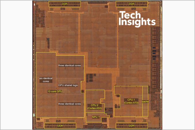
SoC die shot image & labels courtesy of TechInsights Mate 10 teardown
As aforementioned one of the bigger improvements of the Kirin 970 is the switch to a TSMC 10FF manufacturing node. While 10nm is supposed to be a long-lived node for Samsung's foundry – where indeed we’ll see two full generations of SoCs produced on 10LPE and 10LPP – TSMC is taking a different approach and sees its own 10FF process node a short-lived node and stepping-stone to the much anticipated 7FF node, which is to be introduced later in 2018. As such the only TSMC 10FF mobile products to date have been the low-volume MediaTek X30 and Apple 10X in summer and the high-volume Apple A11 and HiSilicon Kirin 970 in Q3-Q4, a 2-3 quarter after Samsung had entered high-volume production of the Snapdragon 835 and Exynos 8895.
HiSilicon’s expectations of the new process node are rather conservative improvement of only 20% in efficiency at the same performance point for the apples-to-apples CPU clusters, below ARM’s earlier predictions of 30%. This rather meagre improvement in power will be likely one of the reasons why HiSilicon decided not to increase the CPU clocks on the Kirin 970, instead focusing on bringing down power usage and lowering the TDP when compared to the Kirin 960.
The SoC does enjoy a healthy die size shrink from 117.72mm² down to 96.72mm² even though the new SoC has 50% more GPU cores as well as new IP blocks such as the NPU. Our colleagues at TechInsights have published a detailed per-block size comparison between the Kirin 960 and Kirin 970 and we see a 30-38% decrease in block size for apples-to-apples IP. The Cortex-A73 quad-core cluster now comes in at only 5.66mm², a metric to keep in mind and in stark contrast to Apple which is investing twice as much silicon area in its dual-core big CPU cluster.
CPU Performance: SPEC2006
SPEC2006 has been a natural goal to aim for as a keystone analysis benchmark as it’s a respected industry standard benchmark that even silicon vendors use for architecture analysis and development. As we saw SPEC2017 released last year SPEC2006 is getting officially retired on January 9th, a funny coincidence as we now finally start using it.
As Android SoCs improve in power efficiency and performance it’s now becoming more practical to use SPEC2006 on consumer smartphones. The main concerns of the past were memory usage for subtests such as MCF, but more importantly sheer test runtimes for battery powered devices. For a couple of weeks I’ve been busy in porting over SPEC2006 to a custom Android application harness.
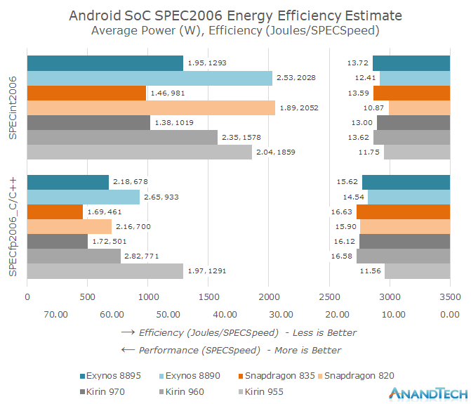
The results are quite remarkable as we see both the generational performance as well as efficiency improvements from the various Android SoC vendors. The Kirin 970 in particular closes in on the efficiency of the Snapdragon 835, leapfrogging the Kirin 960 and Exynos SoCs. We also see a non-improvement in absolute performance as the Kirin 970 showcases a slight performance degradation over the Kirin 960 – with all SoC vendors showing just meagre performance gains over the past generation.
Going Into The Details
Our new SPEC2006 harness is compiled using the official Android NDK. For this article the NDK version used in r16rc1 and Clang/LLVM were used as the compilers with just the –Ofast optimization flags (alongside applicable test portability flags). Clang was chosen over of GCC because Google has deprecated GCC in the NDK toolchain and will be removing the compiler altogether in 2018, making it unlikely that we’ll revisit GCC results in the future. It should be noted that in my testing GCC 4.9 still produced faster code in some SPEC subtests when compared to Clang. Nevertheless the choice of Clang should in the future also facilitate better Androids-to-Apples comparisons in the future. While there are arguments that SPEC scores should be published with the best compiler flags for each architecture I wanted a more apples-to-apples approach using identical binaries (Which is also what we expect to see distributed among real applications). As such for this article the I’ve chosen to pass to the compiler the –mcpu=cortex-a53 flag as it gave the best average overall score among all tested CPUs. The only exception was the Exynos M2 which profited from an additional 14% performance boost in perlbench when compiled with its corresponding CPU architecture target flag.
As the following SPEC scores are not submitted to the SPEC website we have to disclose that they represent only estimated values and thus are not officially validated submissions.
Alongside the full suite for CINT2006 we are also running the C/C++ subtests of CFP2006. Unfortunately 10 out of the 17 tests in the CFP2006 suite are written in Fortran and can only be compiled with hardship with GCC on Android and the NDK Clang lacks a Fortran front-end.
As an overview of the various run subtests, here are the various application areas and descriptions as listed on the official SPEC website:
| SPEC2006 C/C++ Benchmarks | ||||||
| Suite | Benchmark | Application Area | Description | |||
| SPECint2006 (Complete Suite) |
400.perlbench | Programming Language | Derived from Perl V5.8.7. The workload includes SpamAssassin, MHonArc (an email indexer), and specdiff (SPEC's tool that checks benchmark outputs). | |||
| 401.bzip2 | Compression | Julian Seward's bzip2 version 1.0.3, modified to do most work in memory, rather than doing I/O. | ||||
| 403.gcc | C Compiler | Based on gcc Version 3.2, generates code for Opteron. | ||||
| 429.mcf | Combinatorial Optimization | Vehicle scheduling. Uses a network simplex algorithm (which is also used in commercial products) to schedule public transport. | ||||
| 445.gobmk | Artificial Intelligence: Go | Plays the game of Go, a simply described but deeply complex game. | ||||
| 456.hmmer | Search Gene Sequence | Protein sequence analysis using profile hidden Markov models (profile HMMs) | ||||
| 458.sjeng | Artificial Intelligence: chess | A highly-ranked chess program that also plays several chess variants. | ||||
| 462.libquantum | Physics / Quantum Computing | Simulates a quantum computer, running Shor's polynomial-time factorization algorithm. | ||||
| 464.h264ref | Video Compression | A reference implementation of H.264/AVC, encodes a videostream using 2 parameter sets. The H.264/AVC standard is expected to replace MPEG2 | ||||
| 471.omnetpp | Discrete Event Simulation | Uses the OMNet++ discrete event simulator to model a large Ethernet campus network. | ||||
| 473.astar | Path-finding Algorithms | Pathfinding library for 2D maps, including the well known A* algorithm. | ||||
| 483.xalancbmk | XML Processing | A modified version of Xalan-C++, which transforms XML documents to other document types. | ||||
| SPECfp2006 (C/C++ Subtests) |
433.milc | Physics / Quantum Chromodynamics | A gauge field generating program for lattice gauge theory programs with dynamical quarks. | |||
| 444.namd | Biology / Molecular Dynamics | Simulates large biomolecular systems. The test case has 92,224 atoms of apolipoprotein A-I. | ||||
| 447.dealII | Finite Element Analysis | deal.II is a C++ program library targeted at adaptive finite elements and error estimation. The testcase solves a Helmholtz-type equation with non-constant coefficients. | ||||
| 450.soplex | Linear Programming, Optimization | Solves a linear program using a simplex algorithm and sparse linear algebra. Test cases include railroad planning and military airlift models. | ||||
| 453.povray | Image Ray-tracing | Image rendering. The testcase is a 1280x1024 anti-aliased image of a landscape with some abstract objects with textures using a Perlin noise function. | ||||
| 470.lbm | Fluid Dynamics | Implements the "Lattice-Boltzmann Method" to simulate incompressible fluids in 3D | ||||
| 482.sphinx3 | Speech recognition | A widely-known speech recognition system from Carnegie Mellon University | ||||
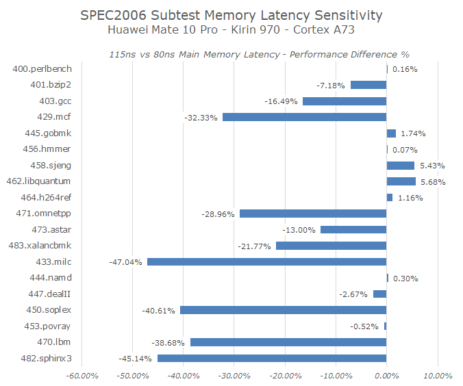
It’s important to note one extremely distinguishing aspect of SPEC CPU versus other CPU benchmarks such as GeekBench: it’s not just a CPU benchmark, but rather a system benchmark. While benchmarks such as GeekBench serve as a good quick view of basic workloads, the vastly greater workload and codebase size of SPEC CPU stresses the memory subsystem to a much greater degree. To demonstrate this we can see the individual subtest performance differences when solely limiting the memory controller frequency, in this case on the Mate 10 Pro with the Kirin 970.
An increase in main memory latency from just 80ns to 115ns (Random access within access window) can have dramatic effects on many of the more memory access sensitive tests in SPEC CPU. Meanwhile the same handicap essentially has no effect on the GeekBench 4 single-threaded scores and only marginal effect on some subtests of the multi-threaded scores.
In general the benchmarks can be grouped in three categories: memory-bound, balanced memory and execution-bound, and finally execution bound benchmarks. From the memory latency sensitivity chart it’s relatively easy to find out which benchmarks belong to which category based on the performance degradation. The worst memory bound benchmarks include the infamous 429.mcf but alongside we also see 433.milc, 450.soplex, 470.lbm and 482.sphinx3. The least affected such as 400.perlbench, 445.gobmk, 456.hmmer, 464.h264ref, 444.namd, 453.povray and with even 458.sjeng and 462.libquantum slightly increasing in performance pointing out to very saturated execution units. The remaining benchmarks are more balanced and see a reduced impact on the performance. Of course this is an oversimplification and the results will differ between architectures and platforms, but it gives us a solid hint in terms of separation between execution and memory-access bound tests.
As well as tracking performance (SPECspeed) I also included a power tracking mechanisms which relies on the device’s fuel-gauge for current measurements. The values published here represent only the active power of the platform, meaning it subtracts idle power from total absolute load power during the workloads to compensate for platform components such as the displays. Again I have to emphasize that the power and energy figures don't just represent the CPU, but the SoC system as a whole, including interconnects, memory controllers, DRAM, and PMIC overhead.
Alongside the current generation SoCs I also included a few predecessors to be able to track the progress that has happened over the last 2 years in the Android space and over CPU microarchitecture generations. Because the runtime of all benchmarks is in excess of 5 hours for the fastest devices we are actively cooling the phones with an external fan to ensure consistent DVFS frequencies across all of the subtests and that we don’t favour the early tests.
SPEC2006 - Full Results
The below chart might be a bit crowded but it it’s the only correct way to have a complete overview of the performance-power-efficiency triad of measurement metrics. The left axis dataset scales based on efficiency (Subtest total energy in joules / subtest SPECspeed score) and also includes the average active power usage (Watts) over the duration of the test. Here the shorter the bars the better the efficiency, while average power being a secondary metric but still should be below a certain value and well within the thermal envelope of a device. The right axis scales simply with the estimated SPECspeed score of the given test, the longer the bar the better the performance.
While the article is focused around the Kirin 970 improvements this is an invaluable opportunity to look back and the two last generations of devices from Qualcomm and Samsung. There is an immediate striking difference in the efficiency of the Snapdragon 820 and Snapdragon 835 across almost all subtests. The comparison between the Exynos 8890 and Snapdragon 820 variants of the S7 was an interesting debate at the time and we came to the conclusion the Exynos 8890 variant was the better unit as it offered longer battery life at higher performance. We see this represented in this dataset as well as the Exynos 8890 manages to have a measurable performance lead in a variety of tests while having higher energy efficiency, albeit a higher power envelope.
2017’s Galaxy S8 reversed this position as the Snapdragon 835 was clearly the better performing unit while having a slight battery life advantage. This efficiency delta can again be seen here as well as the Exynos 8895 isn’t able to compete with the lower power consumption of the Snapdragon 835, even though the performance differences between the Exynos M2 and Cortex A73 are a lot more of a wash than the previous generation’s battle between Exynos M1 and Kryo CPUs.
Switching over to the Kirin SoCs I included as far back as the Kirin 955 with the Cortex A72 as it was a very successful piece of silicon that definitely helped Huawei’s device portfolio for 2016. Remembering our coverage of the Cortex A73 microarchitecture we saw a lot of emphasis from ARM on the core’s floating point and memory subsystem performance. These claims can be easily confirmed when looking at the massive IPC gains in the memory access sensitive tests. When it comes to pure integer execution throughput the A72’s three-wide decoder as expected still managed to outpace the 2-wide unit on the A73 as seen in the 445.gobmk and 456.hmmer subtests.
The Kirin 960 was not able to always demonstrate ARM’s A73’s efficiency gains as again the more execution bound tests the Kirin 955 was equal or slightly more efficient. But again thanks to the new memory subsystem the A73 is able to well distance itself from the A72 with massive gains in 429.mcf, 433.milc, 450.soplex and 482.sphinx3. Again the power figures here are total platform active power so it’s also very possible that the Kirin 960’s memory controller could have a hefty part in the generational improvement.
The Kirin 970 doesn’t change the CPU IP, however we see the introduction of LPDDR4X on the memory controller side which will improve I/O power to the DRAM by lowering the voltage from 1.1V down to 0.6V. While performance should be the same power efficiency should thus be higher by the promised 20% that HiSilicon quotes from the switch to the TSMC 10nm process, plus some percentage due to LPDDR4X.
Performance indeed is within spitting distance of the Kirin 960, however it managed to be a few percentage points slower. On the power efficiency side we see large gains averaging up to 30% across the board. It looks that HiSilicon decided to invest all the process improvement into lowering overall power as the Kirin 970 manages to shave off a whole watt from the Kirin 960 both in integer and floating point benchmarks.
An interesting comparison here is the duel between the Snapdragon 835 and Kirin 970 – both A73 CPUs running at almost identical clocks, one manufactured on Samsung’s 10LPE process and the other on TSMC’s 10FF process. Again by making use of the various workload types we can extract information on the CPU and the memory sub-system. In 445.gobmk and 456.hmmer we see the Kirin have a very slight efficiency advantage at almost identical performance. This could be used as an indicator that TSMC’s process has a power advantage over Samsung’s process, something not too hard to imagine as the latter silicon was brought to market over half a year later.
When we however take a look at more memory bound tests we see the Snapdragon 835 overtake the Kirin 970 by ~20%. The biggest difference is in 429.mcf which is by far the most demanding memory test, and we see the Snapdragon 835 ahead by 32% in performance and a larger amount in efficiency. We can thus strongly assume that between the K970 and S835, Qualcomm has better and more efficient memory controller and subsystem implementation.
The memory subsystem generally seems to be the weak point of Samsung’s Exynos 8895. The M2 core remains competitive in execution bound tests however quickly falls behind in anything more memory demanding. The odd thing here is that I’m not sure if the reason here is memory controller inefficiency but rather something more related to the un-core of the M2 cluster. Firing up even integer power-viruses always have an enormous 1-core power overhead compared to the incremental power cost of additional threads on the remaining 3 cores. A hypothesis here is that given Samsung’s new Exynos 9810 makes use of a completely new cache hierarchy (all but confirmed a DynamiQ cluster) that the existing implementation in the M1 and M2 cores just didn’t see as much attention and design effort compared to the CPU core itself. Using a new efficient cluster design and continuing on improving the core might be how Samsung has managed to find a way (Gaining power and efficiency headroom) to double single-threaded performance in the Exynos 9810.
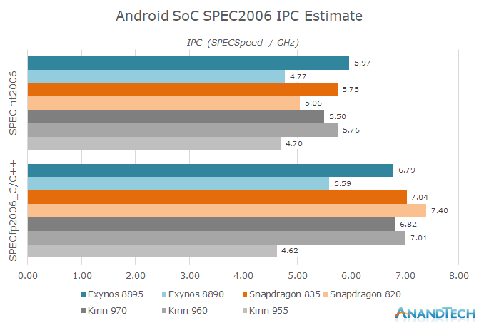
When overviewing IPC for SPEC2006, we see the Kirin 960 and Snapdragon 835 neck in neck, with the Kirin 970 being just slightly slower due to memory differences. The Exynos 8895 shows a 25% IPC uplift in CINT2006 and 21% uplift in CFP2006 whilst leading the A73 in overall IPC by a slight 3%.
The Snapdragon 820 still has good showing in terms of floating point performance thanks to Kryo’s four main “fat” execution pipelines can all handle integer as well as floating point operations. This theoretically should allow the core to have far more floating point execution power than ARM and Samsung’s cores, and is the explanation as to why 470.lbm sees such massive performance advantages on Kryo and brings up the overall IPC score.
The Final Overview
For a final overview of performance and efficiency we get to a mixed bag. If solely looking at the right axis with overall SPECspeed estimated results of CINT2006 and CFP2006, we see that performance hasn’t really moved much, if at all, over the last 2 generations. The Kirin 970 is a mere 10% faster than the Kirin 955 in CINT, over 2 years later. CFP sees larger gains over the A72 but again we come back to a small performance regression compared to the Kirin 960. If one would leave it at that then it’s understandable to raise the question as to what exactly is happening with Android SoC performance advancements.
For the most part, we’ve seen efficiency go up significantly in 2017. The Snapdragon 835 was a gigantic leap over the Snapdragon 820, doubling efficiency at a higher performance point in CINT and managing a 50% efficiency increase in CFP. The Exynos 8895 and Kirin 970 both managed to increase efficiency by 55% in CINT and the latter showed the same improvements in CFP.
This year’s SoCs have also seen a large decrease in average power usage. This bodes well for thermal throttling and flow low thermal envelope devices, as ARM had touted at the launch of the A73. The upcoming Snapdragon 845 and A75 cores promise no efficiency gains over the A73, so the improved performance comes with linear increase in power usage.
I’m also not too sure about Samsung’s Exynos 9810 claiming such large performance jumps and just hope that those peak 2.9GHz clocks don’t come with outrageous power figures just for the sake of benchmark battling with Apple. The Exynos’ 8890 2-core boost feature was in my opinion senseless as the performance benefit of the additional 300MHz was not worth the efficiency penalty (The above results were run at the full 2.6GHz, 2.3GHz is only 10% slower but 25% more efficient) and the whole thing probably had more to do with matching the Snapdragon 820’s scores in the flawed GeekBench 3.
I’m not too sure how to feel about that as I think the current TDPs of the Snapdragon 835 and Kirin 970 (in CPU workloads) are sweet spots that the industry should maintain as it just gives a better mobile experience to the average user, so I do really hope the Snapdragon 845 offers some tangible process improvements to counter-act the micro-architectural power increase as well as clock increases otherwise we’ll see power shooting up again above 2W.
GPU Performance
For 3D graphics and games the Kirin 970 is the first GPU to make use of ARM’s second generation Bifrost GPU architecture, Heimdall / G72. The new IP is an evolutionary update over last year’s Mali G71 with density and efficiency updates.
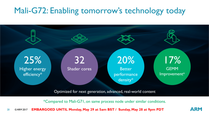
The density increase as well as the process node shrink allowed HiSilicon to increase the GPU core count by 50% from 8 to 12 while still reducing the GPU block complex in terms of absolute silicon area. There is no mincing around with words on last year’s G71 performance: The GPU unfortunately came nowhere near the projected efficiency goals stated by ARM in neither the Exynos 8895 nor the Kirin 960. The Kirin 960 especially was remarkable in terms of how we saw devices powered by it reach until then unheard of average power figures at the peak performance states, ranging at around the 9W mark for the Mate 9. I still remember 2 years ago I had praised HiSilicon for implementing a GPU conservative enough that it could properly sustain its maximum performance state within the device thermal envelope, staying below 4W. Nevertheless before continuing the power argument any power figures of the Kirin 970, let’s go over the peak performance figures of the most commonly used industry 3D benchmarks.
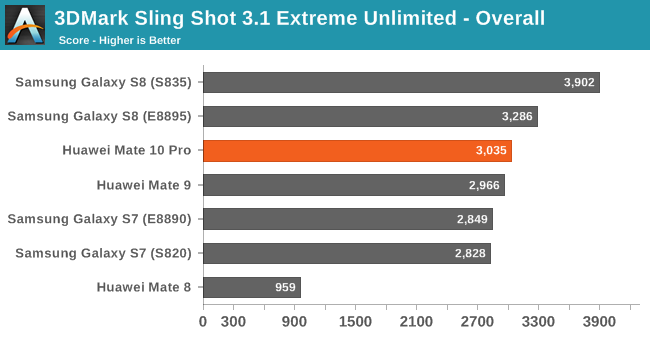
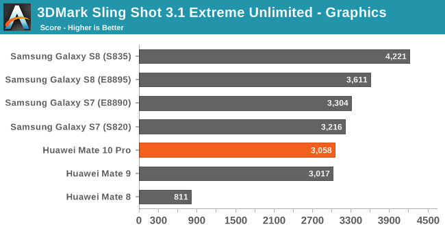
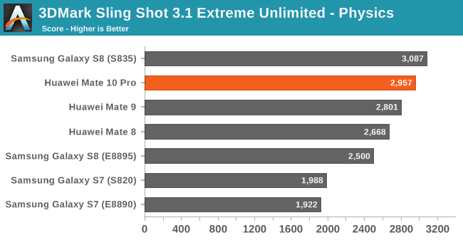
In 3DMark Sling Shot 3.1 Extreme Unlimited we see the G72 on the Kirin 970, oddly enough, not improving at all. I ran the benchmark several times and made sure thermals weren’t the causen but still the phone wasn’t able to increase performance over the Kirin 960 save for a small increase in the physics score. I’m not yet sure what the cause is here – I wasn’t able to monitor GPU frequency as I haven’t rooted the device yet so I can’t be sure that it’s using some kind of limitation mechanism.
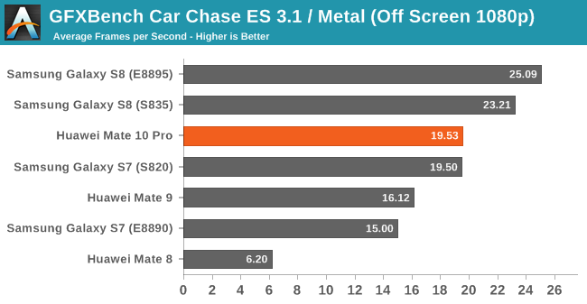
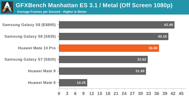
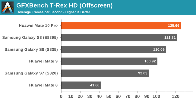
Moving on to Kishonti’s GFXBench we see the Kirin 970 achieve its theoretical gains of 15-20%. As a reminder while the GPU core count increased 50% from 8 to 12 cores, the frequency has been vastly reduced from the maximum 1033MHz down to 746MHz, leaving only a more marginal performance upgrade to be expected.
The Kirin 970’s G71MP12 ends up slightly below the Exynos 8895’s G71MP20 and the Snapdragon 835’s Adreno 540 in more compute bound workloads such as Manhattan 3.1 or Car Chase. In TRex the GPU has a slight lead over the Exynos 8895, but only when the device is cool as it quickly starts throttling down from its maximum frequencies at slightly more elevated temperatures.
GPU Power Efficiency
| GFXBench Manhattan 3.1 Offscreen Power Efficiency (System Active Power) |
||||
| Mfc. Process | FPS | Avg. Power (W) |
Perf/W Efficiency |
|
| Galaxy S8 (Snapdragon 835) | 10LPE | 38.90 | 3.79 | 10.26 fps/W |
| LeEco Le Pro3 (Snapdragon 821) | 14LPP | 33.04 | 4.18 | 7.90 fps/W |
| Galaxy S7 (Snapdragon 820) | 14LPP | 30.98 | 3.98 | 7.78 fps/W |
| Huawei Mate 10 (Kirin 970) | 10FF | 37.66 | 6.33 | 5.94 fps/W |
| Galaxy S8 (Exynos 8895) | 10LPE | 42.49 | 7.35 | 5.78 fps/W |
| Meizu PRO 5 (Exynos 7420) | 14LPE | 14.45 | 3.47 | 4.16 fps/W |
| Nexus 6P (Snapdragon 810 v2.1) | 20Soc | 21.94 | 5.44 | 4.03 fps/W |
| Huawei Mate 8 (Kirin 950) | 16FF+ | 10.37 | 2.75 | 3.77 fps/W |
| Huawei Mate 9 (Kirin 960) | 16FFC | 32.49 | 8.63 | 3.77 fps/W |
| Huawei P9 (Kirin 955) | 16FF+ | 10.59 | 2.98 | 3.55 fps/W |
In terms of average platform active power consumption, the Mate 10 shows as significant improvement over last year’s Mate 9. In Manhattan we go down from 8.6W to 6.33W. In terms of efficiency at similar peak performance the Kirin 970 managed only slightly outpace the Exynos 8895 and Mali G71. The architectural improvements that the G72 is promised to bring is counter-acted by the fact that the Exynos uses more cores at lower frequencies (and efficient voltages), with both ending up at a similar performance and efficiency point. The same effect applies between the Kirin 960 and 970, but in reverse. Here the addition of more cores at a lower frequency amplifies the process and architectural efficiency gains versus the G71, resulting in an absolute efficiency gain of 57% at peak performance, which comes near to Huawei’s stated claims of 50% efficiency gain. It’s to be noted that the true efficiency gain at same performance points is likely near the 100% mark, meaning for the same peak Kirin 960 performance levels the Kirin 970 and G72 implementation will be nearly double its efficiency.
Whilst this all might sound optimistic in terms of performance and efficiency gains, it’s all rather meaningless as the Mate 10 and Kirin 970 average power drains are still far above sustainable thermal envelopes at 6.3W.
| GFXBench T-Rex Offscreen Power Efficiency (System Active Power) |
||||
| Mfc. Process | FPS | Avg. Power (W) |
Perf/W Efficiency |
|
| Galaxy S8 (Snapdragon 835) | 10LPE | 108.20 | 3.45 | 31.31 fps/W |
| LeEco Le Pro3 (Snapdragon 821) | 14LPP | 94.97 | 3.91 | 24.26 fps/W |
| Galaxy S7 (Snapdragon 820) | 14LPP | 90.59 | 4.18 | 21.67 fps/W |
| Galaxy S8 (Exynos 8895) | 10LPE | 121.00 | 5.86 | 20.65 fps/W |
| Galaxy S7 (Exynos 8890) | 14LPP | 87.00 | 4.70 | 18.51 fps/W |
| Huawei Mate 10 (Kirin 970) | 10FF | 127.25 | 7.93 | 16.04 fps/W |
| Meizu PRO 5 (Exynos 7420) | 14LPE | 55.67 | 3.83 | 14.54 fps/W |
| Nexus 6P (Snapdragon 810 v2.1) | 20Soc | 58.97 | 4.70 | 12.54 fps/W |
| Huawei Mate 8 (Kirin 950) | 16FF+ | 41.69 | 3.58 | 11.64 fps/W |
| Huawei P9 (Kirin 955) | 16FF+ | 40.42 | 3.68 | 10.98 fps/W |
| Huawei Mate 9 (Kirin 960) | 16FFC | 99.16 | 9.51 | 10.42 fps/W |
Again on T-Rex, which is less ALU heavy and more texture, fill-rate and triangle rate bound we see the Kirin 970 reach impressive performance levels at impressively bad power figures. At 7.93W the phone doesn’t seem to be able to sustain the peak frequencies for long as even on a second consecutive run we see performance go down as thermal throttling kicks in. So while the Kirin 970 slightly outpaces the Exynos 8895 in performance it does so at 25% lower efficiency.
Against the Kirin 960 as again the previous paragraph might sound dire, it’s a vast improvement in comparison. So disastrous was the peak power of the Mate 9 that still at 28% higher peak performance, the Mate 10 still manages to be 53% more efficient, again validating Huawei’s marketing claims. At iso-performance again I estimate that the Kirin 970 is likely near twice as efficient over the Kirin 960.
In all this you’ll have probably noticed Qualcomm consistently at the top of the charts. Indeed over the last few generations it seems Qualcomm is the only company which has managed to increase performance by architectural and process node improvements without ever increasing and exploding the power budget. On the contrary, Qualcomm seems to steadily able to lower the average power generation after generation, reaching an extremely impressive 3.5-3.8W on the Snapdragon 835. It’s widely quoted that mobile GPU’s power budget is 1.5-2W, but over the last few years the only high-end GPU able to achieve that seems to be Adreno, and this gap seems to be ever increasing generation after generation.
In my review of the Mate 8 there were a lot of users in the comments section who still deemed the performance of the T880MP4 in the Kirin 950 unsatisfactory and uncompetitive. Unfortunately this view is the common widespread notion among most users and most media, and was one of main complaints of Huawei devices in the past. Today Huawei is able to compete at the top of the benchmarks, but at a rather ghastly hidden cost of efficiency and unsustainable power that is perfectly honest a lot harder to test and to communicate to users.
AnandTech is also partly guilty here; you have to just look at the top of the page: I really shouldn’t have published those performance benchmarks as they’re outright misleading and rewarding the misplaced design decisions made by the silicon vendors. I’m still not sure what to do here and to whom the onus falls onto. As long as vendors keep away from configuring devices with unreachable and unsustainable performance states on 3D workloads and keep within reasonable levels then the whole topic becomes a non-issue. If things don’t improve then we’ll have to have a hard look on how to handle these situations I’m considering simply no longer posting any GPU peak performance figures in device reviews and keeping them in separate more technical SoC pieces such as this one.
Overall I think we’re at a critical point in time for the mobile GPU landscape. Qualcomm currently holds such an enormous lead in performance, density and efficiency that other silicon vendors who rely on IP vendors for their GPUs are in a tight and precarious situation in terms of their ability to offer competitive products. I see this as a key catalyst as to why Apple has stated to planning to abandon Imagination as their GPU IP provider in upcoming SoCs and why Samsung has accelerated efforts to replace Mali and also introduce their in-house S-GPU maybe as early as 2019. Over the course of the next 2 years we’ll be seeing some exciting shake-ups of the SoC GPU space, that’s for sure.
An Introduction to Neural Network Processing
AI is currently the big buzzword when talking about consumer electronics. While marketing departments all over are trying to embrace the term, when we’re talking about the current use of AI in computing terms we’re specifically talking about machine learning. More precisely when talking about the latest generations of silicon IPs, we’re talking about the implementation of specialized hardware block which are optimized to run convolutional neural networks (CNNs).
While explaining how convolutional neural networks work in detail is far beyond this piece, they have been a research topic since the 1980’s. The idea is to try to simulate the behaviour of the human brain’s neurons. The keyword here again is simulation; no the various neural network IP’s hardware implementations do not mimic the human brain structure. While the field of neural networks in academia has been around for a long time, it’s only been in the last decade with the introduction software implementations that are able to run on GPUs that things have literally accelerated to become a lot more interesting. Via breakthroughs over the last half-decade, we’ve seen researchers iterate and develop CNN models that improve in terms of accuracy and efficiency.
Looking under the hood, it turns out that CNNs map pretty well to highly threaded execution models. The work itself has minimal branching or other "complex" behavior that requires a general purpose processor (CPU), and instead can typically be broken up into discrete, semi-independent threads. Furthermore the required computational accuracy is not all that high – running fully developed networks can be done via low-precision integers in some cases – again simplifying the scope of the problem. As a result, CNN research & development hit its stride earlier this decade when GPUs began shipping with the necessary compute features and the overall performance to resolve complex CNN execution in a reasonable-by-human-standards timeframe.
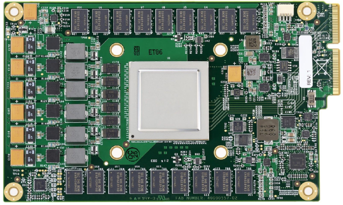
Of course, while GPUs have been the most adapted to running them, GPUs are not the only kind of highly parallel processor out there. As the field is evolving and companies want to commercialize their use in actual use-cases, we saw the need for much higher performance requirements as well as consideration for power efficiency. At this point we started seeing the move towards more specialized processing units whose architecture is built with machine learning in mind. Google was the first to announce such hardware with the announcement of the TPU back in 2016. More specialized hardware loses some flexibility, but in turn it gains power and area (die space) efficiency by only including the hardware and features necessary for the task.
There are two key aspect to actually running NN workloads: first you have to have a trained model which contains the actual information that describes the data that the model is later meant to be run on. The training of models is rather processor intensive – not only is it a lot of work to begin with, but it has to be done with greater levels of precision than the execution of those models, which is to say that efficient neural network training requires more powerful and complex hardware than executing neural networks. Consequently, the idea is that the bulk of models will be trained by high performance hardware, such as server-class GPUs and specialized hardware such a Google’s TPUs on servers in the cloud.
The second aspect of NN is the execution the models; taking the completed models, feeding them new data, and generating results based on what the model perceives. The execution of a neural network model with input data to get an output result is called inferencing. And not unlike the conceptual differences between training and inferencing, the compute requirements for inferencing are quite a bit different as well. The name of the game is still highly parallel compute, but it can be done with lower precision computations and the overall amount of performance required for timely execution is lower as well. Which means that inference can be done on cheaper hardware in many more locations and scenarios.
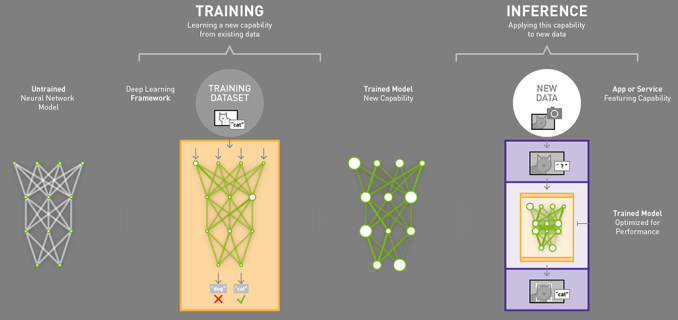
Graphic source: Nvidia Blog
This in turn has caused the industry to move towards inferencing on edge devices (consumer devices) because it’s a much more performant and power efficient. If you have your trained model on your device locally you can just use the processing power of the device to run the inference and avoid having to upload data to the cloud and have a server do it. This alleviates issues such as latency, bandwidth, and power consumption but also eliminates privacy concerns as the input data never leaves your device.
With the goal of running neural network inferencing locally on an edge device, we have the choice of running the implementation on various different processing blocks on devices such as a smartphone. CPU, GPU and even DSPs are all able to run inferencing tasks, however there are vast efficiency differences between them. General purpose CPUs are the least suited for the task as they are not designed with massive parallelised execution in mind. GPUs and DSPs are much better choices but even then there’s much room for improvement. It is here were we see a new class of processing accelerator like the NPU on the Kirin 970.
As these new IP blocks are still new the industry hasn’t had time to agree on a common nomenclature. HiSilicon/Huawei have coined the term NPU/neural processing unit while Apple publicly uses NE/neural engine. Other IP providers such as Cadence/Tensilica just outright call their implementation a neural network DSP (Vision C5), Imagination Technologies (Series 2NX) uses the term NNA/neural network accelerator and CEVA’s NeuPro settled on the marketing friendly “AI processor”. In the sense of simplicity I’ll just continue to refer to them as neural network IPs.
In the case of the Kirin 970 the NPU is provided by a new Chinese IP provider called Cambricon. The Kirin 970 NPU however isn’t a straight off-the-shelf offering but rather a co-development between Cambricon and HiSilicon optimized to HiSilicon’s requirements. Huawei quotes 2 TeraOPS FP16 performance on the IP, however this metric is misleading as the performance figure quotes sparse equivalent peak data, meaning the 8-bit quantized throughput. At this point in time we should largely shy away from theoretical performance figures of the neural network IPs as they don’t necessarily correlate to actual performance and there’s less understood architectural characteristics of the IPs that can play larger roles for the resulting end-performance.
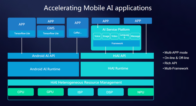
The first hurdle to using a neural network on a hardware block other than the CPU is to make use of the proper APIs to access that block. The SoC and IP vendors all currently ship proprietary APIs and SDKs to enable application development for using hardware acceleration for neural networks. In the case of HiSilicon they offer the HiAI API which can manage the workloads between CPU, GPU and NPU. The API is currently not publicly available as it’s still under development, but developers which reach out to HiSilicon can get early access before the public release later in the year. Vendors such as Qualcomm make available the SNPE (Snapdragon Neural Processing Engine) SDK which does the equivalent task of enabling app developers to tap into resources of the GPU and DSP for neural network processing workloads. Other IP vendors of course have their own SDKs for their respective IPs.
However vendor-specific APIs may end up being a temporary quirk of the present time; the goal in the future is to have a common universal API alongside the respective vendor’s IPs. Google has already been working on this and the NN API introduced in Android 8.1 is already actively shipping on Pixel 2 devices. One note that I’ve been made aware of is that currently the NN API only supports a subset of features that is available to IP like the NPU, so for developers to take full advantage of the hardware and extract maximum performance Huawei still sees application developers targeting the various proprietary APIs while using the NN API as a fall-back method.
NPU Performance Tested
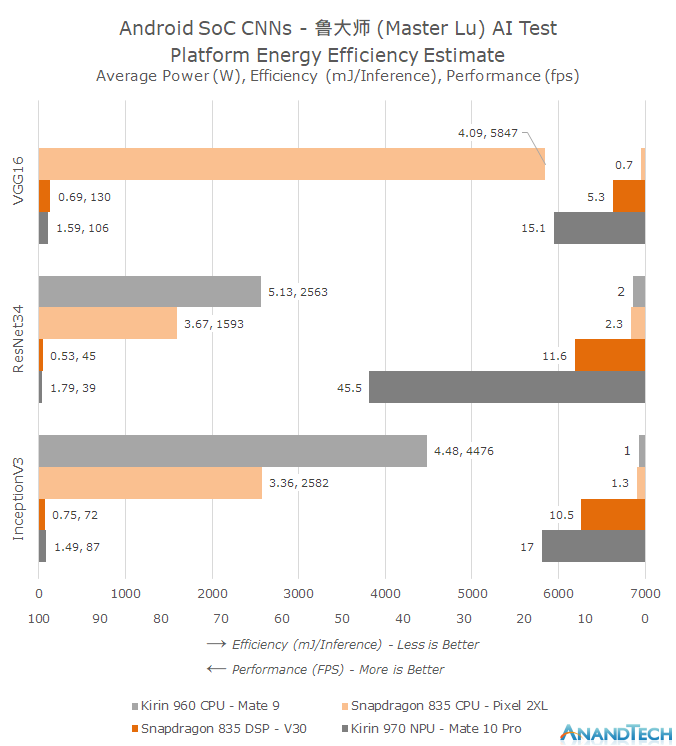
To test the performance of the NPU we need a benchmark which currently targets all of the various vendor APIs. Unfortunately at this stage short of developing our own implementation the choices are scarce, but luckily there is one: Popular Chinese benchmark suite Master Lu recently introduced an AI benchmark implementing both HiSilicon’s HiAI as well as Qualcomm’s SNPE frameworks. The benchmarks implements three different neural network models: VGG16, InceptionV3 as well as ResNet34. The input dataset are 100 images which are a subset of the ImageNet reference database. As a fall-back the app implements the TensorFlow inferencing library to run on the CPU. I’ve ran the performance figures on the Mate 10 Pro, Mate 9 as well as two Snapdragon 835 (Pixel 2 XL & V30) devices respectively running on the CPU as well as the Hexagon DSP.
Similarly to the SPEC2006 results I chose to use a more complex graph to better showcase the three dimensions of average power (W), efficiency (mJ/inference) as well as absolute performance (fps / inferences per second).
First thing we notice from the graph is that we can observe an order of magnitude difference in performance between the NPU and CPU implementations. Running the networks as they are on the CPUs we’re not able to exceed 1-2fps and we do so at very heavy CPU power consumption. Both the Snapdragon 835 as well as the Kirin 960 CPUs struggle with the workloads with average power exceeding sustainable workloads.
Qualcomm’s Hexagon DSP is able to improve on the CPU performance by a factor of 5-8x. But Huawei’s NPU performance figures are again several factors above that, showcasing up to a 4x lead in ResNet34. The reason for the different performance ratio differences between the different models is their design. Convolutional layers are heavily parallelisable whilst the polling and fully connected layers of the models must use more serial processing steps. ResNet in particular makes use of a larger percentage of convolution processing for a single inference and thus is able to achieve a higher utilization rate of the Kirin NPU.
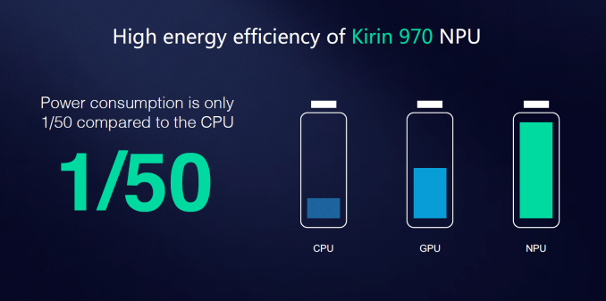
In terms of power efficiency we’re very near to Huawei’s claims of up to a 50x improvement. This is the key characteristic that will enable CNNs to be used in real-world use-cases. I was quite surprised to see Qualcomm’s DSP reach similar efficiency levels as Huawei’s NPU – albeit at 1/3rd to 1/4th of the performance. This should bode quite well in terms of the Snapdragon 845’s Hexagon 685 which promises up to a 3x increase in performance.
I wanted to take the opportunity to make a rant about Google’s Pixel 2: I was able to actually run the benchmark on the Snapdragon 835’s CPU because the Pixel 2 devices lacked support for the SNPE framework. This was in a sense maybe both expected as well as unexpected. With the introduction of the NN API in Android 8.1, which the Pixel 2 phones support and use acceleration through the dedicated Pixel Visual Core SoC, it’s natural that Google would want to push usage of Android’s standard APIs. But on the other hand this is also a limitation on the capabilities of the phone by the OEM vendor which I can’t help but compare to the decision by Google to by default omit OpelCL in Android. This is a decision which in my eyes has heavily stifled the ecosystem and is why we don’t see more GPU accelerated compute workloads, out of which CNNs could have been one.
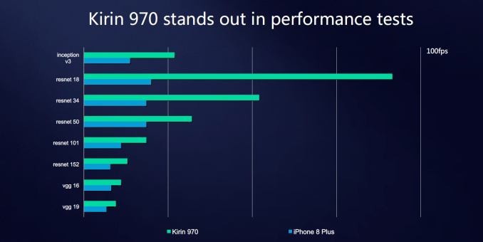
While we can’t run the Master Lu AI test on an iPhone, HiSilicon did publish some slides with reported internally numbers we can try to correlate. Based on the models included in the slide, the Apple A11 neural network IP’s performance should land somewhere slightly ahead of the Snapdragon 835’s DSP but still far behind the Kirin NPU, but again we can't independently verify these figures due to lack of a fitting iOS benchmark we can run ourselves.
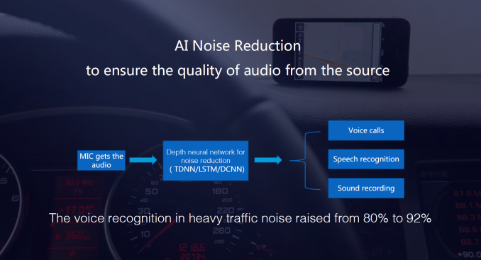
Of course the important question is, what is this all good for? HiSilicon discloses that one use-case being used is noise reduction via CNN processing, and thus is able to increase voice recognition rate in heavy traffic from 80% to 92%.
The other most publicised use-case is the implementation in the camera app. The Mate 10’s camera makes use of the NPU to run inferencing to recognize different scenarios and optimize the camera settings based on pre-sets for those scenarios. The Mate 10 comes with a translation app which was developed with Microsoft, which is able to use the NPU for accelerated offline translation, and this was definitely the single most impressive usage for me. Inside the built-in gallery application we also see the use of image classification to create a new section where pictures are organized by content type. The former scenarios where the SoC is doing live inferencing on a media stream such as the camera feed is also the use-case where HiSilicon has an advantage over Qualcomm as employs both a DSP and the NPU whereas Snapdragon SoCs have to share the DSP resources between vision processing and neural network inferencing workloads.
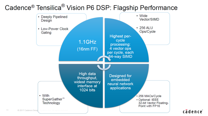
Oddly enough the Kirin 970 has sort of double the silicon IP capable of running neural network efficiently as its vision pipeline also includes a Cadence Tensilica Vision P6 DSP which should be in the same performance class as Qualcomm’s Hexagon 680 DSP, but is currently not exposed for user applications.
While the Mate 10 does make some use of the NPU it’s hard to argue that it’s a definitive differentiating factor for the end-user. Currently neural network usage in mobile doesn’t seem to have the same killer-applications that they have in automotive and security camera sectors. Again this is due to the ecosystem being its early days and the Mate 10 among the first devices to actually offer such a dedicated acceleration block. It’s arguable if it’s worth it for the Kirin 970 to have implemented such a piece and Huawei is very open about the fact that it’s reaching out to developers to try and find more use-cases for the silicon, and at least Huawei should be lauded for innovating with something new.
Huawei/Microsoft's translation app seemed to be the most distinguished experience on the Mate 10 so maybe there’s more non-image based use-cases that can be explored in the future. Currently the app allows the traditional snapshot of a foreign language text and then shows a translated overlay, but imagine a future implementation where it’s able to do it live from the camera feed and allow for an AR experience. MediaTek at CES also showed a distinguishing use-case of using CNNs: for video conferencing the video encoder is fed metadata on scene composition by a CNN layer doing image recognition and telling the encoder to use finer-grained block sizes where a user’s face would be, thus increasing video quality. It’s more likely that neural network use-cases will slowly creep up with time rather than there being a new revolutionary thing, as more devices will start to incorporate such IPs and they become more widespread so will developers be more enticed to find uses for them.
Final Thoughts
What I wanted to showcase with this article was not only the particular advances of the Kirin 970, but also to use it as an opportunity to refresh everyone on the competitive landscape of the high-end Android SoC market. As the modern, post-iPhone smartphone ecosystem enters its 10-year anniversary, we’re seeing the increasing consolidation and vertical integration of the silicon that power today’s devices.
I wouldn’t necessarily say that Apple is the SoC trend setter that other companies are trying to copy, as much as other vendors are coming to the same conclusion Apple has: to be able to evolve and compete in a mature ecosystem you need to be able to control the silicon roadmap yourself. Otherwise you fall into the risk of not being able to differentiate from other vendors using similar component stacks, or risk not being competitive against those vendors who do have vertical integration. Apple was early to recognize this, and to date Huawei has been the only other OEM able actually realize this goal towards quasi-silicon independence.
I say quasi-independence because while the companies are designing their own SoCs, they are still relying on designs from the big IP licensing firms for key components such as the CPUs or GPUs. The Kirin 970 for example doesn’t really manage to differentiate itself from the Snapdragon 835 in regards to CPU performance or efficiency, as both ARM Cortex-A73 powered parts end up end up within margins of error of each other.
Snapdragon 820’s Kryo CPU core was a hard sell against a faster, more efficient, and smaller Cortex-A72. Samsung’s custom CPU efforts fared slightly better than Qualcomm’s, however the Exynos M1 and M2 haven’t yet managed to present a proper differentiating advantage against ARM’s CPUs. Samsung LSI’s performance claims for the Exynos 9810 are definitely eye-brow raising and might finally mark the point where years of investment and development on a custom CPU truly pay off, but Samsung’s mobile division has yet to demonstrate true and committed vertical integration. Considering all of this, HiSilicon’s decision to stick with ARM CPUs makes sense.
While Qualcomm has backpedalled on using its custom CPU designs in mobile, the company does demonstrate the potential and advantages of controlling your own IP designs when it comes to the GPU. To draw parallels, on the desktop GPU side of things we already see the competitive and market consequences of one vendor having a ~33% efficiency advantage (Nvidia GeForce GTX 1080 vs AMD Radeon Vega 64). Just imagine that disparity increasing to over 75-90%, and that’s currently the state that we have in the mobile landscape (Snapdragon 835 vs Kirin 970). In both cases silicon vendors can compensate for efficiency and performance by going with a larger GPU, something that is largely invisible to the experience of the end-user but definitely an unsustainable solution as it eats into the gross margin of the silicon vendor. With PPA disparities on the high end nearing factors of 4x it definitely gives moment to pause and wonder where we’ll be heading in the next couple of years.
Beyond CPU, GPU and modem IP, SoCs have a lot more component blocks that are generally less talked about. Media blocks such as encoder/decoders eventually end up summarized as feature-checkboxes going up to X*Y resolution at Z frames per second. Even more esoteric are the camera pipelines such as the ISPs of modern SoCs. Here the lack of knowledge of how they work of what the capabilities are both part due to the silicon vendor’s secrecy but also due to the fact that currently truly differentiating camera experiences are defined by software algorithm implementations. The Kirin 970’s new use a Cadence Tensilica Vision P6 DSP definitely uplifts the camera capabilities of the devices powered by the new SoC, but that’s something that we’ll cover in a future device-centric review.
The NPU is a new class of IP whose uses are still in its infancy. Did the Kirin 970 need to have it included to be competitive? No. Does its addition make it more competitive? Yes. Well, maybe. With the software ecosystem lagging behind it’s still early to say how crucial neural network acceleration IPs in smartphones will become, and we have sort of a chicken-or-egg sort of situation where certain use-cases might simply not be feasible without the hardware. The marketing advantages for Huawei have been loud and clear, and it looks industry wide adoption is inevitable and on its way. I don’t foresee myself recommending or not recommending a device based on its existing, or lack of “AI” capabilities for some time to come, and similarly consumers should apply a wait & see approach to the whole topic.
While going on a lot of tangents and comparisons against competitors, the article’s main topic was the Kirin 970. HiSilicon’s new chipset proves itself as an excellent smartphone SoC that's well-able to compete with Qualcomm’s and Samsung’s best SoCs. There’s still a looming release schedule disadvantage as Huawei doesn’t follow the usual spring Android device refresh cycle, and we expect newer SoCs to naturally leapfrog the Kirin 970. This might change in the future as both semiconductor manufacturing and IP roadmaps might become out of sync with the spring device product launches.
I come back to the fact that Huawei is only one of two OEM vendors – and the only Android vendor – whom is leveraging vertical integratation between their SoC designs and the final phones. The company has come a long way over the past few years and we’ve seen solid, generational improvements in both silicon as well as the complete phones. What is most important is that the company is able to put both reasonable goals and execute on its targets. Talking to HiSilicon I also see the important trait of self-awareness of short-comings and the need to improve in key areas. Intel’s Andy Grove motto of “only the paranoid survive” seems apt to apply to Huawei as I think the company is heading towards the right directions in the mobile business and a key reason for their success.

