Original Link: https://www.anandtech.com/show/1210
Socket 940 Roundup: Motherboards for the Athlon64 FX
by Wesley Fink on December 18, 2003 1:39 PM EST- Posted in
- Motherboards
While the Athlon64 FX is clearly the fastest processor currently available, several developments have made finding motherboards to use with these FX chips something of a problem. First of all, the FX chip has had very limited availability until recently. Now, we are seeing greater quantities of the expensive FX chips, but even those few manufacturers producing Socket 940 boards have been caught with out-of-stock product because they underestimated AMD production. Second, the Socket 940 Athlon64 FX requires Registered DDR 400 memory instead of the more common unbuffered DDR that most already own. This became an even bigger handicap when AMD let it be known at the 9/23 introduction that the FX would be launched in a new 939 socket version in the first half of 2004. The new Socket 939 version will allow use of regular unbuffered memory instead of the more expensive, harder-to-find registered DDR memory required by 940 boards. It now seems that the 939 should appear somewhere in the March/April 2004 time frame.
Whatever the liabilities of the Socket 940 Athlon64 FX motherboards, there is no disputing that the Enthusiast community has recently embraced the FX chip. Recently, an FX-based board was the first to crack 30,000 on the FutureMark 2001SE Hall of Fame. With this kind of attention to the FX processor, and about 3 to 4 months until Socket 939, it was time for a closer look at the performance of Socket 940 motherboards.
When AMD launched the Athlon64 FX on September 23rd, the only motherboard readily available was the Asus SK8N, a board developed for the Opteron and based on the nVidia nForce3-150 Pro chipset. The MSI K8T Master, which was also developed for the Opteron and based on the VIA chipset, also went through some revision and emerged as an FX motherboard. AnandTech evaluated the MSI board in its review of the ElitePC Titan FX gaming system. Gigabyte also introduced a Socket 940 board for the FX, and we reviewed the nF3-150 Pro Gigabyte K8NNXP-940 in October. Asus has recently introduced a second Socket 940 motherboard, based on the VIA chipset, called the SK8V. The SK8V is just now entering the marketplace.
These 4 motherboards are the only Socket 940 motherboards that you will likely find for sale. A few others like Leadtek have shown Socket 940 products, but they have been very difficult or impossible to find, at least in the US. There also have been many BIOS revisions to these boards as they have developed and matured. In fact, these seemingly endless updates have delayed this Socket 940 roundup several times as we ended up retesting boards with the latest BIOS update, offering improved performance and added features. Our goal is to find the best Athlon64 FX board that you can buy. Is there a clear winner among the four motherboards that can be bought for the top-of-the-line FX processor?
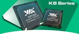
A Closer Look at nForce3 150 Pro and VIA K8T800
We took a close look at the single-channel nForce3 150 and K8T800 in our launch review of Athlon64 Motherboards. The biggest distinction of the Socket 940 FX compared to the Socket 754 Athlon64 is the support of Dual-Channel memory. However, the memory controller for Athlon64 processors is on the processor itself, which makes the differences between chipsets for 940 and 754 fairly minimal — much less than would be seen with a chipset-based memory controller.
nVidia's nForce3 PRO is the only Athlon64/Athlon64 FX/Opteron chipset in a single-chip package. Both VIA K8T800 and SiS755 use the more familiar Northbridge/Southbridge arrangement. Key Features for nForce3 PRO are:
- Single-Chip Solution — Revolutionary single-chip solution designed for the AMD Opteron CPU enables higher-quality, full-featured motherboards and delivers maximum performance with the lowest latency. The single-chip design also means less power consumption and less heat dissipation.
- Dual-Channel DDR400 Memory — Full support for Dual-Channel DDR Registered ECC memory, and the Athlon64 version also supports non-ECC memory.
- 64-Bit Architecture — NVIDIA nForce3 Pro provides advanced processing capabilities and system innovations for the new 64-bit AMD processor architecture.
nVidia will soon introduce the nForce3 250 and 250 PRO chipsets, which they say will fully implement the 800 HT bus at full 16-bit speed, and will include support for SATA and SATA RAID. The nF3 150 is dated in terms of features, and nVidia promises that this will be corrected in the 250 incarnation.
One of the most interesting features of the Athlon64/Athlon64 FX/Opteron is AMD's decision to include the memory controller on the CPU. For a chipset maker, the move of the memory controller to the CPU itself means that the chipset design is much simplified. In fact, about half of the requirements of the supporting chipset are eliminated, which allows a much simpler design. VIA chose to use a traditional North Bridge/South Bridge design instead of a single chip solution. However, VIA also added many features to the chipset like SATA RAID.
Key Features of VIA K8T800
- Supports full range of AMD Opteron/Athlon64/FX processors
- Hyper8 Technology enables 16-bit/1.6GHz HyperTransport processor-to-chipset link
- Support for AGP 8X/4X
- V-Link 533 MB/sec high bandwidth North/South Bridge interconnect
- Support for VIA Vinyl 5.1 & Vinyl Gold 7.1 Multichannel Audio Suite
- Serial ATA support for up to 4 devices
- Integrated V-RAID with RAID 0, RAID 1
- Parallel ATA133/100/66 support for up to 4 devices
- Support for up to 8 USB 2.0/USB 1.1 ports, UHCI compliant
- Support for VIA Gigabit Ethernet controller & Integrated 10/100 Fast Ethernet
- Integrated MC'97 Modem
The VIA K8T800 is a very contemporary chipset when combined with the VT8237 Southbridge. By offering SATA, SATA RAID, 8 USB 2.0, and ATA133, the feature set of the K8T800, unlike the nF3-150, is comparable to any of the best Intel boards on the market. While manufacturers have added supplementary chips to nF3-150 boards to make their boards competitive, the K8T800/VT8237 provides most of these same features with the chipset. Although the upcoming 250 chipset will bring features back into balance, for now, the VIA K8 solution has a much better feature mix than nVidia.
In the Athlon64 roundup we found no performance difference between nVidia and VIA on the single-channel A64 motherboards. However, nVidia boards did overclock further, apparently because of their ability to fix the PCI/AGP bus in BIOS. The Athlon64 chips are locked, or at the very least, “top-locked”. This means that you cannot presently exceed the stated multiplier of Athlon64 chips. However, there are utilities and even BIOS options on some boards that allow lower multipliers to be selected. All of this means that the ability to run a “locked” PCI/AGP — or Asynchronous bus — allows for better performance on motherboards designed for the Athlon64.
It is important to understand that the Athlon64 FX is quite different, since AMD, from the beginning, has emphasized that this “Enthusiast” processor is unlocked. With the ability to select both higher and lower multipliers on the FX, the choice to fix AGP/PCI is much less important. Many also do not understand that, despite what you have read, the Opteron 1xx and Athlon64 FX do differ in one very important way. The Athlon64 FX is unlocked and multipliers can be adjusted; the Opteron 1xx is multiplier locked and ratios can not be adjusted. This is a very important distinction if you plan to overclock your processor to achieve higher performance levels.
Basic Features: Socket 940 Motherboards
| Motherboard Specifications | ||
| Asus SK8N | Gigabyte K8NNXP-940 | |
| CPU Interface | Socket 940 AMD Athlon64 FX and Opteron | |
| Chipset | nVidia nForce 3 150 | |
| Bus Speeds | 200 to 300MHz (in 1MHz increments) | |
| PCI/AGP Speeds | Auto, or Fixed | Auto, or Fixed 66-100 (in 1 MHz increments) |
| Available CPU Ratios | 4.0 to 20.0 in 0.5 increments | 4.0 to 25.0 in 0.5 increments |
| Core Voltage | 1.075V - 1.775V in 0.025V increments | 0.8V - 1.7V in 0.025V increments |
| DRAM Voltage | 2.5V – 2.7V in 0.1V increments | Normal, +0.1, +.2, +.3V |
| AGP Voltage | 1.5V to 1.7V in 0.1V increments | Normal, +0.1, +.2, +.3V |
| Chipset Voltage | No Adjustment | Normal, +0.1, +.2, +.3V |
| Memory Slots | Four 184-pin DDR DIMM Slots Dual-Channel Configuration Registered or Registered ECC DDR to 4GB Total |
|
| Expansion Slots | 1 AGP 8X Slot 5 PCI Slots |
|
| Onboard Serial ATA/RAID | Promise PDC20378 (2 Drives, 0, 1) |
Silicon Image Sil3112 supports Raid 0/1 |
| Onboard IDE/RAID | Two ATA133/100/66 (4 devices) Plus Promise PDC20378 (2 Drives, RAID 0, 1) |
Two ATA133/100/66 (4 devices) Plus 2 GigaRAID ATA133 IDE RAID 0, 1, 0+1 |
| Onboard USB 2.0/IEEE-1394 | 6 USB 2.0 ports by nF3 2 1394a (400 MB/s) FireWire ports |
6 USB 2.0 ports by nF3 TI 1394B (800 MB/s) FireWire (2 ports) |
| Onboard LAN | CK8 Realtek RTL8201BL 10/100 LAN | DUAL LAN, Realtek Gigabit LAN + Realtek 10/100 LAN |
| Onboard Audio | Realtek ALC650 codec | Realtek ALC658 codec AC '97 2.3 6-Channel with UA |
| BIOS Revision | 1004 (12/09/03) | F3 (10/23/03) |
| Motherboard Specifications | ||
| Asus SK8V | MSI K8T Master-FAR | |
| CPU Interface | Socket 940 AMD Athlon64 FX and Opteron | |
| Chipset | VIA K8T800 Northbridge, VIA VT8237 Southbridge | |
| Bus Speeds | 200 to 300MHz (in 1MHz increments) | 200 to 233MHz (in 1MHz increments) |
| PCI/AGP Speeds | No Adjustment | No Adjustment |
| Available CPU Ratios | 800 - 4000MHz in 100MHz increments | Not Adjustable |
| Core Voltage | 0.80V – 1.75V in 0.025V increments | Fixed, Not Adjustable |
| DRAM Voltage | Auto, 2.6V to 2.8V in 0.1V increments |
Fixed, Not Adjustable |
| AGP Voltage | 1.5V, 1.7V in 0.1V increments |
Fixed, Not Adjustable |
| Chipset Voltage | VLink, 2.5V, 2.6V | Not Adjustable |
| Memory Slots | Four 184-pin DDR DIMM Slots Dual-Channel Configuration Registered or Registered ECC DDR to 4GB Total |
|
| Expansion Slots | 1 AGP 8X Slot 5 PCI Slots, WiFi Slot |
1 AGP 8X Slot 4 PCI Slots |
| Onboard Serial ATA/RAID | VIA 8237 (2 Drives, 0, 1) Promise PDC20378 (2 Drives, 0,1) |
VIA 8237 (2 Drives, 0, 1) |
| Onboard IDE/RAID | 8237 (4 drives ATA133) Promise PDC20378 (2 Drives, 0, 1) |
8237 (4 drives ATA133) No IDE RAID |
| Onboard USB 2.0/IEEE-1394 | 8 USB 2.0 ports by 964 2 1394a FireWire ports |
6 USB 2.0 ports by 8237 No FireWire ports |
| Onboard LAN | 3Com 3C940 Gigabit LAN | Broadcom Gigabit LAN |
| Onboard Audio | ADI AD1985 SoundMax 6-Channel with SPDIF |
AC '97 2.2 Audio |
| BIOS Revision | Beta 1002.018 (11/23/03) | 1.1 (11/07/03) |
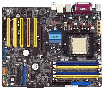
Asus SK8N: Board Layout and Features
The Asus SK8N was one of the first boards to be introduced for the Opteron. However, as a single CPU board, the SK8N has gone through many BIOS revisions and has evolved into a feature-rich Athlon64 FX board. The latest 1004 BIOS completes the transition with a wide range of multipliers and voltages for the FX Enthusiast.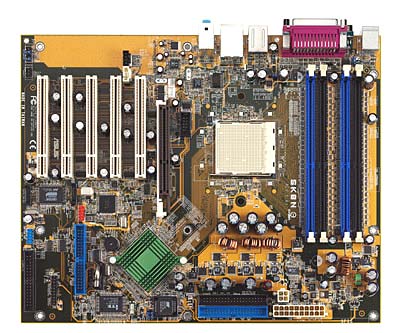
The Asus SK8N is a full-size, ATX 3-phase design with plenty of room for an effective layout of the on-board options. The basic layout of the board is a bit different than usually seen; the CPU is in the middle of the board and the 4 memory slots are at the top of the board, instead of the more commonly seen upper-right location. In general, the layout works quite well with only 1 complaint.
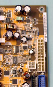
The 20-pin ATX connector and the 4-pin 12 volt connector are both in our preferred upper right position. The location of the memory at the top of the board removes all chances of interference with the 8X AGP slot, and will work well in most designs except those with extra CPU cooling just below the Power Supply.
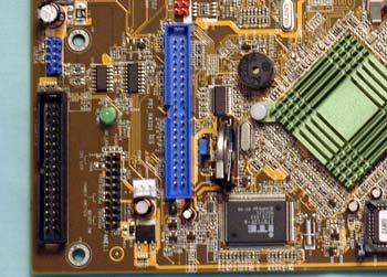
The only issue in the board design is the location of the floppy, which is at the bottom right of the motherboard. Since the SK8N is designed for the Enthusiast Athlon64 FX chip, this board is more likely to be used in a full tower. In some tower designs, this will be an issue.
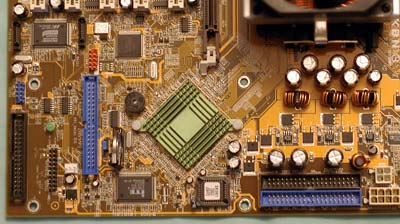
The IDE connectors, IDE RAID, and 2 SATA connectors are all in good locations. They should present no problems in most case designs.
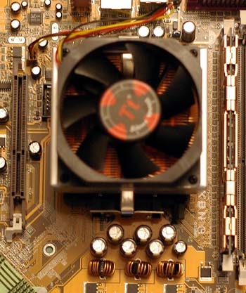
With the CPU in the middle of the board, it should be an easy task to have enough room for just about any heatsink/fan that you can imagine. Certainly, there will be no problems with standard Socket 754/940 coolers. There was no problem mounting any of the HSF on hand, including the huge Zalman CNPS7000.
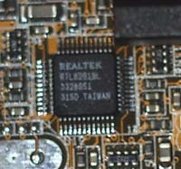
LAN is provided by the Realtek RTL8201BL chip.
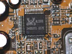
Since the SK8N design is one of the older Asus designs, we see the Realtek ALC650 used for audio. This is an acceptable solution if audio is not a critical issue, but it is not at the same quality level as the more recent 100db S/N ratio Realtek ALC658 or the ADI SoundMax seen on more recent Asus designs.
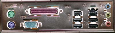
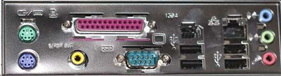
I/O port offerings on the SK8N are good, if a bit puzzling. It is unlikely that Asus planned for an integrated video model of the SK8N, so the missing serial port is a puzzle. Included are 4 USB 2.0 ports, LAN, Firewire, Parallel, one serial, 3 mini audio jacks, and PS2 keyboard and mouse ports. Two additional brackets are included: one provides a single Firewire port, and the other provides 2 USB 2.0 ports. An additional audio bracket is not included.
Asus SK8N: BIOS and Overclocking
BIOS
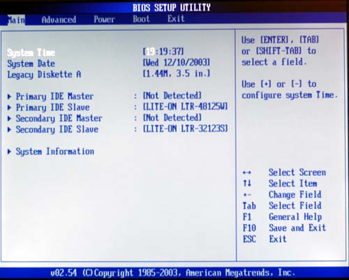
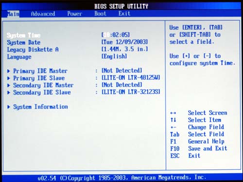
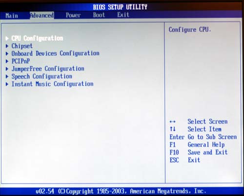
Asus uses AMI BIOS on almost all of their current boards, including the SK8N. Major categories are across the top and each category has many submenus.
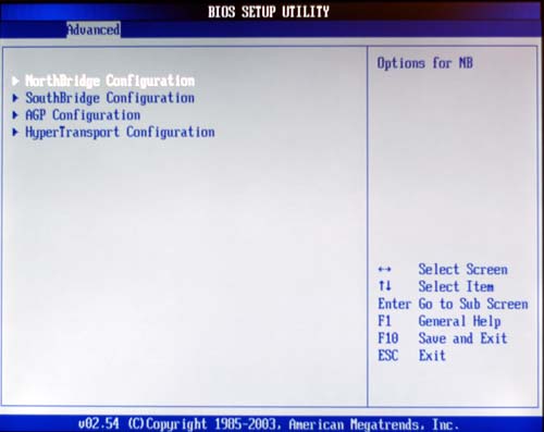
Most of the adjustment options that we normally use are in the Advanced section, which includes Northbridge Configuration, Southbridge Configuration, AGP Configuration, and HyperTransport Configuration.
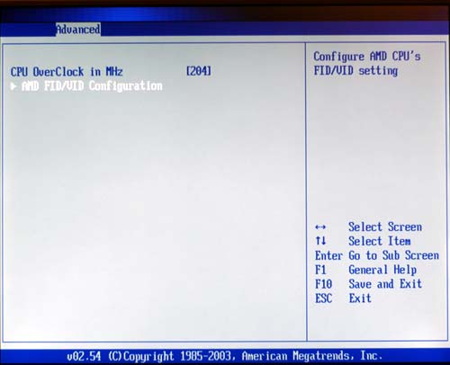
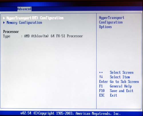
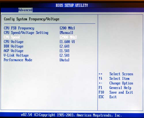
While the SK8N has a reorganized BIOS to improve understanding, even the 1004 BIOS for the SK8N still uses an arrangement that can be confusing. Adjustments for multipliers and voltage are under “Advanced” in the “AMD FID/VID Configuration” sub-menu.
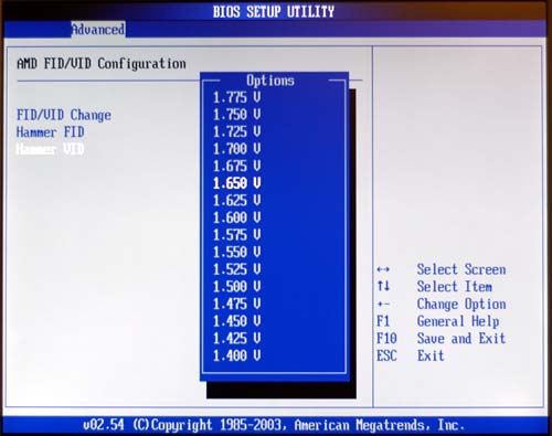
While there is an overall CPU voltage adjustment in another menu, the fine tuning is done in the “Hammer VID” submenu.
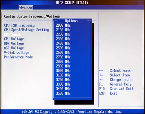
Multipliers can be adjusted in the “Hammer FID” submenu. A wide range from 4 to 20 is available with half multipliers. As already mentioned, Asus has reworked the arrangement and descriptions in the SK8V BIOS that we will be examining later. Unfortunately, the SK8N arrangement is just as obscure as ever.
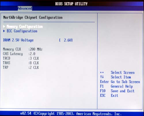
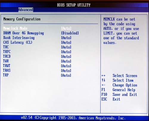
Adjustments for memory are under “Advanced”, “Northbridge Chipset Configuration”. Once you locate them, you will find a complete range of memory timing adjustments, but a limited vDIMM range to 2.7V.
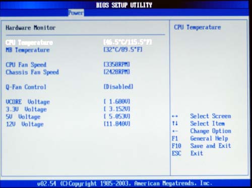
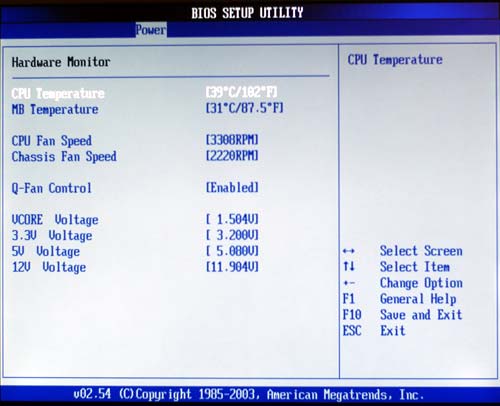
PC Health information is very complete, and can be found under the Power Menu, “Hardware Monitor” submenu. You will find system temperatures, fan speeds, and voltages. There are also controls for the Asus Q-fan utility, which enables fan speeds to be controlled by temperature.
FSB Overclocking Results
We have not found the Athlon64 FX to be a particularly good overclocker, which is not a surprise for a new top-line processor. However, with the recent Asus SK8N BIOS updates, we were able to squeeze more from the FX than we have seen in the past.| Front Side Bus Overclocking Testbed | ||
| Default Voltage | Maximum Overclock | |
| Processor: | Athlon64 FX51 2.2GHz |
Athlon64 FX51 2.2Ghz |
| CPU Voltage: | 1.5V (default) | 1.65V |
| Cooling: | Cooler Master Silent K8 Heatsink/Fan | Cooler Master Silent K8 Heatsink/Fan |
| Power Supply: | Enermax 465W | Enermax 465W |
| Maximum OC: | 2346MHz (+6.6%) 11x213 |
2452MHz (+11.5%) 12x204 |
The above overclocking setup at default voltage allowed us to reach the highest stable setting of 213 (852 HT). The highest MHz speed achieved was at 12x204 or 2452MHz at 1.65V. Higher overclocks may be possible at higher voltages, but we were not comfortable running greater than 10% voltage increase with air cooling.
The SK8N, particularly with the 1004 BIOS, has the tools needed to overclock an FX processor effectively. The only adjustment that is a bit lacking is memory voltage or vDIMM, which only allows adjustment to 2.7V. This is less of an issue with Registered memory than it might be with standard unbuffered DDR, where many high-end manufacturers are now certifying performance to 3.0V.
Asus SK8N: Stress Testing
We performed stress tests on the Asus SK8N in these areas and configurations:1. Chipset and motherboard stress testing, conducted by running the FSB at 213MHz at default voltage. We also ran a few stability tests at the highest overclock of 2452GHz at 1.65V.
2. Memory stress testing, conducted by running the Registered ECC Memory at 400MHz with 2 Dual-Channel (1 bank) DIMM slots filled, and at 400MHz with all 4 Dual-Channel (2 bank) DIMM slots filled at the lowest memory timings possible with Mushkin Registered ECC 3200 memory. Since the Athlon64 FX does not require ECC for proper operation, all memory tests were run with ECC disabled.
Front Side Bus Stress Test Results:
We ran a full range of stress tests and benchmarks to ensure that the Asus SK8N was absolutely stable at the overclocked speed at default voltage. This included Prime95 torture tests, and the addition of other tasks — data compression, various DX8 and DX9 games, and apps like Word and Excel — while Prime95 was running in the background. At default voltage, 213MHz was the highest overclock that we were able to achieve; 2452MHz was the highest overclock that we could achieve by raising the CPU voltage or Hammer VID to 1.65V.Memory Stress Test Results:
This memory stress test is very basic, as it simply tests the ability of the SK8N to operate at its officially supported memory frequency (400MHz DDR) at the lowest supported memory timings that our Mushkin High Performance ECC Registered Modules will support. The Registered Modules were run at SPD timings:| Stable DDR400 Timings — 2 DIMMs 2/4 DIMMs populated — 1 DC bank |
|
| Clock Speed: | 200MHz |
| Timing Mode: | 128-bit DC |
| CAS Latency: | 2.0 |
| Bank Interleave: | N/A |
| RAS to CAS Delay: | 3T |
| RAS Precharge: | 6T |
| Precharge Delay: | 2T |
| Command Rate: | Auto |
| ECC: | Disabled |
We had no problem running 2 DS 512MB DIMMs of our standard Mushkin ECC Registered in the SK8N at the aggressive SPD timings at default memory voltage.
Filling all available memory banks is more strenuous on the memory subsystem than testing 2 DIMMs, but we had no problem at all running with all 4 matching DIMMs installed providing 2 Dual-Channel Banks.
| Stable DDR400 Timings — 4 DIMMs 4/4 DIMMs populated — 2 DC bank |
|
| Clock Speed: | 200MHz |
| Timing Mode: | 128-bit DC |
| CAS Latency: | 2.0 |
| Bank Interleave: | N/A |
| RAS to CAS Delay: | 3T |
| RAS Precharge: | 6T |
| Precharge Delay: | 2T |
| Command Rate: | Auto |
| ECC: | Disabled |
The required memory timings with 4 DIMMs were the same as 2 DIMMs, the fastest 2-2-3-6 SPD timings of the Mushkin Registered memory. No memory voltage increase was required for stability as the SK8N was stable at default memory voltage with 4 DIMMs.
Prime95 torture tests were successfully run at the timings listed in the above charts. We also ran ScienceMark (memory tests only) and Super Pi. None of the three stress tests created any stability problems for the Asus SK8N at these memory timings and standard memory voltage.
Gigabyte K8NNXP-940: Features and Board Layout
The Gigabyte K8NNXP-940 was reviewed in early October and the full review can be found here. The 6-phase design K8NNXP-940 is one of the most feature-rich motherboards that you can buy for any processor. It is positioned as the Gigabyte flagship design for their extensive Athlon64 motherboard line-up.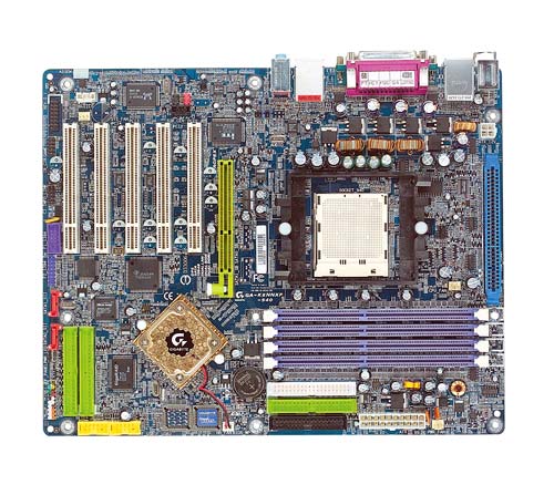
For this Socket 940 roundup, all testing for the K8NNXP-940 was repeated with the latest F3 BIOS and the November release of nVidia nForce platform drivers. In general, performance had changed little from the October review, except in the SPECviewperf 7.1 workstation performance benchmarks. The latest nVidia platform drivers do appear to improve performance significantly in workstation tests.
Asus SK8V: Features and Board Layout
Since Asus often provides Reference Boards for technology introductions, and the Socket 940 SK8N was already available in the marketplace, it was a bit of a surprise to see Asus introduce a new Socket 940 motherboard. The SK8V, based on the competing VIA K8T800 chipset, was an all-new design for Asus, and unquestionably, a risky venture in a limited market segment. With a somewhat limited lifespan expected for boards catering to the Socket 940 version of the Athlon64 FX processor, Asus must be confident that this board will stand out from the competition.The Asus SK8N was one of the first boards to be introduced for the Opteron, and with BIOS revisions, it has remained a very competitive Socket 940 board with a good feature set. However, with the new SK8V, Asus pulled out all the stops and loaded it with all the latest Asus trademark features.
Please refer to the table below for the main difference between SK8V and SK8N.
| SK8V | SK8N | |
| North Bridge | VIA K8T800 VIA VT8237 |
nVidia nForce 3 Pro150 |
| South Bridge | ||
| DDR 400 support | Yes (With Athlon 64 FX) | |
| RAID | Dual RAID (Promise 20378 & VIA 8237) | Promise 20378 |
| Audio chipset | ADI 1985-6CH | ALC650-6CH |
| Gigabit LAN | 3Com 3C940 | CK8 MAC+ Realtek RTL8201BL PHY |
| Max 1394 ports | 2 | 2 |
| Max USB 2.0 ports | 8 | 6 |
| WiFi Slot | Yes | No |
| PCI standard | PCI 2.2 | PCI 2.3 |
As you can see, the SK8V certainly has a different look than most current Asus boards. Instead of the gold/pale brown color that Asus normally uses, the SK8V is finished in all black. The Asus SK8V is a full-size, ATX 3-phase design that is a very different design and layout from the earlier SK8N.
Probably a result of the 2-chip VIA K8T800, the SK8V uses a more familiar layout that is similar to other top motherboards. The only placement that is a bit unique is the CPU socket in the top center instead of the top left as seen in many boards. This allows more room between the CPU and the back of the I/O ports. The layout of the board is a little different than what we normally see, but it was well-conceived and in general, works very well.
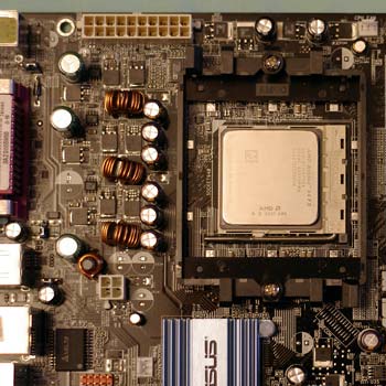
The 20-pin ATX connector and the 4-pin 12 volt connector are both to the left of the CPU instead of our preferred upper right position. However, with more space between the CPU and I/O ports, this does not create a routing problem in our standard tower case. In some designs, this could be a little more of a challenge, so please check your case design to make sure that this placement will work for you. The 4 memory slots on the SK8V are in the more common upper right location. There is plenty of room for adding and removing dimms, and the 8X AGP slot does not interfere with the dimm slots in any way.

The IDE connectors, IDE RAID, floppy, and 4 SATA connectors are all in good locations. The floppy connector is edge-mounted about the middle right of the board, which works well in larger cases, but is disliked by some. None of these locations presented any problems in a full tower design, and should present no problems in most case designs.
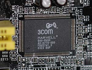
The Asus SK8V uses the familiar 3Com Gigabit LAN seen on many Asus designs.
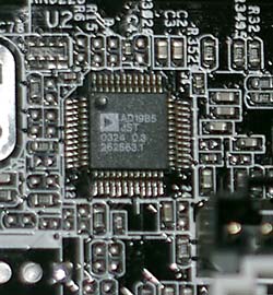
In the continuing upgrades to on-board audio, Asus is using the high-quality Analog Devices SoundMax AD1885 codex to supply 6-channel audio. This is the same chip that Asus uses on its top-end boards, and it is the chip pioneered by Intel on their top 875 boards along with the auto-jack-sensing feature. A Coaxial SPDIF out jack is provided on the rear panel for Dolby Digital setups. More information on the SoundMax audio codec is available at http://www.soundmax.com/.
I/O port offerings on the SK8V include the PS2 ports, SPDIF out, Parallel, Serial, Firewire, 4 USB 2.0 ports, Gigabit LAN, and 3 mini jacks with auto-sensing for up to 6 external speakers. The auto-sensing feature is nice, but keep in mind that with 6 speakers connected, you will no longer have a MIC port available in this configuration. 3 Accessory brackets are included: 4 USB 2.0, 1 Firewire, and SPDIF coax/Optical.
Asus SK8V: BIOS and Overclocking
BIOS
The SK8V uses AMI BIOS, which is seen on most current Asus boards. While the layout of the AMI is quite different from the familiar Award layout, it is really easy to use once you get the hang of the logic. Major categories are across the top and each category has many submenus.
With the 1002.012 and 1002.018 BIOS used for benchmarking, Asus has redesigned the SK8V BIOS so that it will be easier to use. The Advanced section now includes a “JumperFree Configuration” submenu with many of the adjustments that Enthusiasts will be using.
The “Advanced”, “CPU Configuration” sub-menu contains adjustments for HyperTransport and Memory.
Memory Configuration allows adjustment of a complete range of memory timings, as well as the ability to force memory timings.
“Jumperfree Configuration” has settings for CPU and Memory Frequencies and Voltages. Instead of the obscure Hammer FID and Hammer VID names, Asus is using more familiar descriptions like “CPU Speed” and “CPU Voltage”.
Beginning with 1002.012, Asus has added a full range of multipliers to the SK8V, which now includes half multipliers. On the 1002.018 BIOS, you can set speeds form 800MHz to 4000MHz in 100MHz increments.
PC Health information is in the standard Asus location for AMI BIOS. It can be found under the Power Menu, “Hardware Monitor” sub-menu. There, you will find system temperatures, fan speeds, voltages, and the controls for the Asus Q-fan utility, which allows fan speeds to be controlled by temperature.
FSB Overclocking Results
As mentioned in the SK8N section, the latest BIOS' from Asus are restoring our faith in the overclocking abilities of the Athlon64 FX. This is even more true with the recent BIOS' and new options available for the Asus SK8V.| Front Side Bus Overclocking Testbed | ||
| Default Voltage | Maximum Overclock | |
| Processor: | Athlon64 FX51 2.2GHz |
Athlon64 FX51 2.2Ghz |
| CPU Voltage: | 1.5V (default) | 1.625V |
| Cooling: | Cooler Master Silent K8 Heatsink/Fan | Cooler Master Silent K8 Heatsink/Fan |
| Power Supply: | Enermax 465W | Enermax 465W |
| Maximum OC: | 2346MHz (+6.6%) 11x213 |
2475MHz (+12.5%) 11x225 or 12x206 |
The above overclocking setup at default voltage allowed us to reach the highest stable setting of 213 (852 HT). The highest MHz speed achieved was at 11x225/12x206 or 2475MHz at 1.625V. Higher overclocks may be possible at higher voltages, but we were not comfortable running greater than 10% voltage increase with air cooling. These were the highest overclocks that we could achieve up to 1.65V.
Higher overclocks may also be possible using a future BIOS from Asus. We did have some difficulties with random Multiplier/FSB resets on the 018 Beta BIOS. We had no such problem with the 012 BIOS, but the voltage range is not as wide in the 012 BIOS. Asus Engineers are looking at the issues that we found and updates will be incorporated in the release 1002 BIOS.
The range of overclocking options available on the SK8V from BIOS 1002.012 up is truly outstanding. The options also are effective, yielding the highest overclock that we have seen with modest air cooling on this Athlon64 FX. The voltage ranges in the most recent BIOS' are even better than the SK8N and Gigabyte K8NNXP-940, which have been praised for their wide voltage ranges. Asus seems to have found ways to unlock the VIA K8T800 chipset by providing even half multipliers. It had been widely speculated that only the nF3 chipset could do half multipliers, but Asus has proven that this is not the case.
Asus SK8V: Stress Testing
We performed stress tests on the VIA-chipset Asus SK8V in these areas and configurations:1. Chipset and motherboard stress testing, conducted by running the FSB at 213MHz at default voltage. We also ran a few stability tests at the highest overclock of 2475GHz at 1.625V.
2. Memory stress testing, conducted by running the Registered ECC Memory at 400MHz with 2 Dual-Channel (1 bank) DIMM slots filled, and at 400MHz with all 4 Dual-Channel (2 bank) DIMM slots filled at the lowest memory timings possible with Mushkin Registered ECC 3200 memory. Since the Athlon64 FX does not require ECC for proper operation, all memory tests were run with ECC disabled.
Front Side Bus Stress Test Results:
We ran a full range of stress tests and benchmarks to ensure that the Asus SK8V was absolutely stable at the overclocked speed at default voltage. This included Prime95 torture tests, and the addition of other tasks — data compression, various DX8 and DX9 games, and apps like Word and Excel — while Prime95 was running in the background. 213MHz was the highest overclock that we were able to achieve at default voltage; 2475MHz was the highest overclock that we could achieve by raising the CPU voltage or Hammer VID to 1.625V. Raising the voltage to 1.65V did not improve overclocking or stability.Memory Stress Test Results:
This memory stress test simply tests the ability of the SK8V to operate at its officially supported memory frequency (400MHz DDR) at the lowest supported memory timings that our Mushkin High Performance ECC Registered Modules will support. The Registered Modules were run at SPD timings:| Stable DDR400 Timings — 2 DIMMs 2/4 DIMMs populated — 1 DC bank |
|
| Clock Speed: | 200MHz |
| Timing Mode: | 128-bit DC |
| CAS Latency: | 2.0 |
| Bank Interleave: | N/A |
| RAS to CAS Delay: | 3T |
| RAS Precharge: | 6T |
| Precharge Delay: | 2T |
| Command Rate: | Auto |
| ECC: | Disabled |
Two Double-Sided 512MB DIMMs of our standard Mushkin ECC Registered ran with no problem in the SK8V at the aggressive SPD timings and default memory voltage. However, for best stability we needed to raise the memory voltage to 2.6V. At that setting, all testing at 2-2-3-6 was completely stable.
Filling all available memory banks is more strenuous on the memory subsystem than testing 2 DIMMs, but we had no problem running with 4 matching DIMMs installed providing 2 Dual-Channel Banks.
| Stable DDR400 Timings — 4 DIMMs 4/4 DIMMs populated — 2 DC bank |
|
| Clock Speed: | 200MHz |
| Timing Mode: | 128-bit DC |
| CAS Latency: | 2.0 |
| Bank Interleave: | N/A |
| RAS to CAS Delay: | 3T |
| RAS Precharge: | 6T |
| Precharge Delay: | 2T |
| Command Rate: | Auto |
| ECC: | Disabled |
The required memory timings with 4 DIMMs were the same as 2 DIMMs, the fastest 2-2-3-6 SPD timings of the Mushkin Registered memory. For best stability, a memory voltage setting of 2.6V was required, the same setting needed for best stability with 2 DIMMs.
Prime95 torture tests were successful at the timings listed in the above charts. We also ran ScienceMark (memory tests only) and Super Pi. None of the three stress tests created any stability problems for the Asus SK8V at these memory timings and standard memory voltage.
MSI K8T Master2-FAR: Features and Board Layout
The MSI K8T Master is still basically a server board in 1 and 2 processor versions. In fact, you will still find it listed at MSI's web site in their server section. While MSI has made BIOS revisions to allow the K8T Master to work with an Athlon64 FX processor (but not 2 — that distinction is left to Opteron), the board is really in a different category than other boards in this roundup.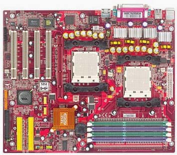
Our recent review of the ElitePC Titan FX, which uses the K8T Master, proves that the board is very fast, but the limited features, lack of voltage adjustments, lack of multiplier adjustments, and limited memory support do not really make it competitive with other boards aimed at the Computer Enthusiast looking for a home for the Athlon64 FX. While the Asus SK8N was also first introduced as an Opteron motherboard, Asus has upgraded the board and continues to add features that make the SK8N competitive with other boards in this roundup.
The MSI K8T Master 2 series are excellent Opteron boards, since multipliers are not supported on Opteron, and this will not be a handicap. Clearly, the inability of the K8T Master 2 to run 4 DIMMs in the Stress Test in the ElitePC review was not a result of any issues with the VIA K8T800 chipset. This is proven by the excellent performance of the Asus SK8V, also based on the K8T800, with 4 DIMMs at the fastest memory speeds available. We suspect that the single CPU version of the K8T Master series may not have any issues running 4 DIMMs. This is speculation, however, until we actually test a single CPU version of the K8T.
Since benchmarks of the MSI K8T Master 2 in the Elite PC Gaming System were run with an ATI Radeon XT 256Mb Video Card in a Dual 10,000 rpm SATA RAID platform, all benchmarks were recompiled for the Socket 940 roundup. Retesting used our standard ATI Radeon 9800 PRO 128mb Video Card and a single 120GB 7200 rpm IDE hard drive.
ASUS: Tech Support and RMA
While we retested all Socket 940 motherboards for this roundup, the two new boards that are included are both from Asus. It therefore made sense to take a look at Asus' Technical Support again since Support and RMA will be a consideration for many trying to decide whether or not to buy an Asus SK8N or SK8V motherboard for their Athlon64 FX.For your reference, we will repost our support evaluation procedure here:
The way our Tech Support evaluation works is first we anonymously email the manufacturer's tech support address(es), obviously not using our AnandTech mail server to avoid any sort of preferential treatment. Our emails (we can and will send more than one just to make sure we are not getting the staff on an “off” day) all contain fixable problems that we have had with our motherboard. We then give the manufacturer up to 72 business hours to respond and then we will report whether or not they responded within the time allotted, and if they were successful in fixing our problems. In case we don't receive a response before the review is published, any future responses will be added to the review, including the total time it took for the manufacturer to respond to our requests.
The idea here is to encourage manufacturers to improve their technical support as well as provide new criteria upon which to base your motherboard purchasing decisions. As motherboards become more similar every day, we have to help separate the boys from the men in as many ways as possible. As usual, we are interested in your feedback on this and other parts of our reviews, so please do email us with your comments.
Things have been changing recently at Asus, and frankly, we were pleasantly surprised to receive a reply from Asus Technical Support in 61 hours. This is the first time in recent memory that Asus has met our 72-hour response deadline. While one incident may be a fluke, we hope this is the first indication that Asus is making changes in their Technical Support procedures. Only consistent performance over time will provide a clear answer.
Several months ago, Asus revised their web site to include a clear and readable RMA policy on their site. We've reposted ASUS' RMA policy for your convenience:
Dear Sir/Madam Please provide the following information so that we may process your request for warranty repair service. Once we have obtained that information from you, we will issue an RMA # and provide the proper shipping instructions. Please read and provide all of the information below. We cannot complete your request, if all of the information below is not provided.This is a reasonably clear RMA policy without all the convoluted wording that could confuse some end users.
Thank you, ASUS Computer International
PLEASE PROVIDE US WITH:ASUS Computer International (USA) is a warranty repair service center. Please contact place of purchase for credit, refund, upgrade, or advance replacement. Asus does not provide these services under any circumstances.
- THE MODEL & SERIAL NUMBER OFF OF YOUR PRODUCT model (name of product) serial# (10 digits/characters long, no dashes).
- YOUR FULL NAME/NAME OF COMPANY (Only provide company name if the shipping address is to a company).
- YOUR SHIPPING ADDRESS (no PO boxes please).
- YOUR DAYTIME PHONE/FAX NUMBER.
ASUS does not cover physical damage. Please refer to page 2 of your users manual. There is a $15.00 fee to replace a broken socket. There is a $40.00 fee to repair all other physical damage. If a product is not repairable, the product will be sent back to the customer. If a product is sent in with physical damage and is not accompanied with a payment, the product will be rejected and customers will not be reimbursed for shipping charges. A payment can be made by check, money order (payable to ASUS), or a credit card#. The payment must be sent in with the damaged product. Customers from Canada must make payments with a credit card #.
The following procedures should be used to contact Asus Support and RMA on the web:
- Click the “contact ASUS” hyperlink on their North American (U.S.) web page.Here, you will find several international contact listings, including the North American contact information, which will read Asus Computer International (AMERICA).
- Click on the http://helpdesk.asus.com hyperlink, which will connect you to their support website. In the lower left hand corner, there will be a hyperlink that reads “ASUS RMA Online”, and three options will appear.
- Go to the option that reads “issue a new RMA online”, where you will be immediately taken to their online RMA form.
ASUS' tech support is also available on the same website as their RMA and warranty information. The ASUS tech support email address is [email protected], or you can try to reach ASUS at (502) 995-0883 in the U.S. Press “3” on your phone for full access. One positive aspect of ASUS' tech support is their phone line hours, which are from 5:30 AM to 5:00 PM (Pacific Standard Time).
Performance Test Configuration
| Performance Test Configuration | |
| Processor(s): | AMD Athlon64 FX51 |
| RAM: | 2 x 512MB Mushkin ECC Registered High Performance 2:3:2 #991125 |
| Hard Drive(s): | Seagate 120GB 7200 RPM (8MB Buffer) |
| Video AGP & IDE Bus Master Drivers: | VIA Hyperion 4.51 (12/02/03) nVidia nForce Platform 3.13 (11/03/03) |
| Video Card(s): | ATI Radeon 9800 PRO 128MB (AGP 8X) |
| Video Drivers: | ATI Catalyst 3.9 |
| Operating System(s): | Windows XP Professional SP1 |
| Motherboards: | Asus SK8N (nVidia nForce3-150 PRO) Gigabyte K8NNXP-940 (nVidia nF3-150 PRO) Asus SK8V (VIA K8T800) MSI K8T Master 2 (VIA K8T800) |
All performance tests were run with the ATI 9800 PRO 128MB video card with AGP Aperture set to 128MB with Fast Write enabled. Resolution in all benchmarks is 1024x768x32.
Benchmarks were run under the same conditions with the same components on the four Socket 940 motherboards with an Athlon64 FX51 processor. For a broader comparison, benchmarks from other AnandTech reviews of Socket 754 Athlon64 motherboards have been included where they were available.
Additions to Performance Tests
We have just updated our test suite to ZD Labs Multimedia Content Creation Winstone 2004 and ZD Labs Business Winstone 2004 for system benchmarking. We have included both Multimedia Content Creation 2003/Business Winstone 2002 and the 2004 version results to assist in comparing to other reviews.Game Benchmarks
We have added Gun Metal DirectX Benchmark 2 from Yeti Labs, the new X2 Benchmark, which includes Transform and Lighting effects, and Aquamark3 to our standard game benchmarks. We will be adding other game benchmarks from our Video Testing Suite in the near future.Content Creation and General Usage Performance
Until the introduction of the Athlon64 series, Content Creation was a benchmark dominated by Intel processors. That is no longer the case, with the Athlon64 FX as the current best performer in both Content Creation and General Usage benchmarks. Since we had seen virtually no difference in chipset performance in our Athlon64 reviews, we were more than a bit surprised to find the VIA K8T800-based boards on top of both Multimedia Content Creation and Office Productivity in this Socket 940 roundup. This was true in both Multimedia Content Creation 2003 and Office Winstone 2002, as well as the latest 2004 versions of the same benchmarks.
One of the big surprises was the substantial drop in scores for the MSI K8T Master2 on the retest with our standard test components. We did not expect such a large drop from benchmarks run on the K8T in the Elite PC review. It is obvious that the 10,000 rpm SATA RAID, ATI Radeon XT 256 Mb, and system tweaks improve Content Creation and General Usage performance significantly. While the VIA-chipset based Asus SK8V is the winner in these benchmarks, the MSI, which also uses the VIA chipset, is virtually the same in performance.
Media Encoding and Gaming Performance
The most recent BIOS upgrades from Asus have really improved gaming performance. The SK8V is now dominant across all gaming benchmarks except GunMetal 2, which produces unusual results on the Socket 940 platforms. If we discard the suspect GunMetal 2 results, the Performance advantage of the SK8V is very clear. With the on-chip Memory Controller of the A64 series, this kind of variation in motherboards was not expected at all. Asus has done an outstanding job with the SK8V as you can see in the gaming benchmarks.
nVidia assured us that the recent 11/03 update to their nForce platform drivers would bring better performance in nF3-150 PRO benchmarks. For that reason, we retested the Gigabyte nF3-150 PRO and re-ran benchmarks with the SK8N to provide the fairest comparison. The 11/03 nVidia drivers made almost no difference in gaming benchmarks, but we did see some improvements in other areas. Our standard Video card for benchmarking is the ATI Radeon 9800 PRO 128Mb. Perhaps we would have seen an improvement in game scores had we tested with a top nVidia card. However, in our standard A64 FX test setup, the nForce3-150 PRO lags behind the K8T800 in gaming and encoding performance.
High End Workstation Performance
The VIA K8T800, in general, and the Asus SK8V, in particular, dominate the Workstation Performance benchmarks. While the biggest improvement in nF3-150 PRO performance with the 11/03 platform drivers is in Workstation Performance benchmarks, the nF3 still lags behind the K8T800 on these high-end boards. The SK8V once again dominates, outperforming the other three Socket 940 boards in every benchmark.
We first ran the SPECviewperf benchmarks several weeks ago. At that time, the SK8V performed very well, but it did not dominate the Workstation Performance tests as we now are seeing. Asus is making some significant improvements in performance with recent SK8V BIOS updates. The enhanced performance has not come by sacrificing stbility, however, as the SK8V has remained stable in all benchmarks.
To understand why the VIA chipset boards were performing better on the A64 FX, we ran several benchmarks at overclocked speeds on both the nF3-150 PRO and the K8T800 boards. The difference that we are seeing at stock speed gets wider at overclocked speeds. This suggests that the increased bandwidth of the A64FX and the demands of overclocking take its toll on the capabilities of the 600HT and 8-bit uplink used in the nForce3-150 PRO. If this is true, it might also explain why we find no difference at all in the performance of the lower-bandwidth mainstream Athlon64 when run on the nF3-150 or K8T800.
Final Words
When AnandTech took a look at Athlon 64 motherboards, we found no difference in the performance of the nVidia nForce3-150 and VIA K8T800 chipsets. Our recommendation for the Athlon64 was to buy the Athlon 64 board with the best features for the money if you planned to run at stock speed. Since the nForce3-150 boards did overclock better on the A64, we recommended the nF3 boards for those planning to overclock.The Athlon64 FX is a completely different ball game, however. nVidia's slower 600 HyperTransport and 8-bit uplink appear to have met their match in the broader bandwidth of the Socket 940 processors. The VIA K8T800-based boards are clear winners at stock speed in our Socket 940 shootout. Perhaps just as important, the top overclocker in the 940 shootout is also the VIA K8T800-based Asus SK8V. In fact, the SK8V's ability to run very well at a 225 setting forces a re-examination of our assumptions about how VIA manages the PCI/AGP bus on the Socket 940 design.
With the memory controller on the Athlon64 FX chip, we really expected the performance of Socket 940 motherboards to be extremely close. Instead, there is a clear winner in the shootout. The Asus SK8V is the best performing, best overclocking, and best featured Socket 940 motherboard. While the MSI K8T Master 2 also performed well in our tests, the very limited Enthusiast features (no multipliers, no voltage adjustments) combined with the inability to run 4 DIMMs with a A64 FX makes the MSI a lesser choice for the Athlon64 FX user. The K8T would be an excellent choice, however, for Opteron users who do not have multipliers, or especially for those planning an Opteron Dually rig.
The nVidia nForce3-150 PRO boards performed well and were quite stable. Where features are most important, the Gigabyte K8NNXP-940, in particular, is hard to ignore. It is the only board in the Socket 940 roundup that even includes the latest “B” version Firewire with the 800MB/s data rate. In the end, though, all of the nForce3-150 PRO motherboards were overshadowed by the incredible performance of the Asus SK8V. nVidia will soon be updating the nForce3 chipset to the Nforce3-250 PRO version, and that will likely change the performance landscape again. We are also expecting the SiS755FX, which should provide competition to both VIA and nVidia.
 |
It is rare to find such a clear winner in a shootout, but the Asus SK8V is that clear winner. It is the Socket 940 board that will please most Computer Enthusiasts aiming to squeeze the most from an Athlon64 FX processor. In fact, the SK8V is the best performing desktop motherboard AnandTech has ever tested. AnandTech is pleased to honor the Asus SK8V with our Gold Editor's Choice as the best motherboard for the Athlon64 FX. |
AMD will launch a revised Athlon64 FX around the end of the first quarter of 2004. The new Socket 939 A64 FX will be able to use the standard unbuffered memory that most Enthusiasts already own instead of the more expensive, harder-to-find Registered memory required by the Socket 940 processors. This will not represent the death of Socket 940, however, since the FX 940 versions will continue and the Opteron will remain a Socket 940 processor. However, it will mean new boards, new revisions, and a new round of performance comparisons. Until March/April 2004, though, the best Athlon64 motherboard you can buy is the Asus SK8V.


