Original Link: https://www.anandtech.com/show/11750/hot-chips-ibms-next-generation-z14-cpu-mainframe-live-blog-5pm-pt-12am-utc
Hot Chips: IBM's Next Generation z14 CPU Mainframe Live Blog (5pm PT, 12am UTC)
by Ian Cutress on August 22, 2017 6:55 PM EST- Posted in
- CPUs
- Enterprise CPUs
- IBM
- IBM z14
- Mainframe
07:56PM EDT - Sitting down, ready to go
08:01PM EDT - This is the last set of talks at Hot Chips. Starting with IBM, then Intel Xeon, AMD EPYC and Qualcomm Centriq
08:02PM EDT - We've covered Xeon, EPYC and Centriq in recent articles, and nothing new is being announced for the show for them except some minor things that we'll summarize in a news post
08:02PM EDT - But the IBM z14 will be interesting
08:02PM EDT - To clarify, the z series is IBM's mainframe product line
08:02PM EDT - So this isn't POWER8 or POWER9
08:04PM EDT - IBM's z-series has central processors and system control chips with integrated fabric and off-compute chip caches
08:05PM EDT - This is under a 'mainframe' setup, rather than a standard CPU/co-processor setup.
08:05PM EDT - Dr Christian Jacobi to the stage, Chief Architect
08:06PM EDT - z14 was technically announced a few weeks ago
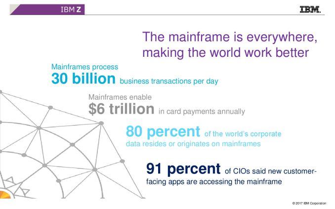
08:06PM EDT - A lot of mainframes still exist
08:06PM EDT - Still used in large corporations for transactional data, e.g. credit card has a mainframe involved. 90% of airline booking systems involve mainframes
08:07PM EDT - Run large databases and large virtualised linux
08:07PM EDT - Have to make design decisions tailored for those workloads
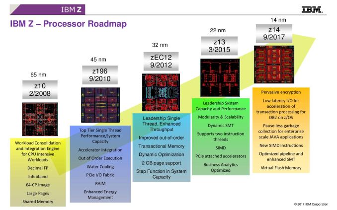
08:07PM EDT - z10 was high frequency, z196 had OoO, z13 had SMT and now z14
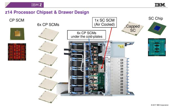
08:08PM EDT - The mainframe uses two different chips - the CP (cores and shared L3) and SCP (large L4 and interconnect logic)
08:08PM EDT - Picture is a deep drawer with DRAM, PCIe, and six CP chips under cold plates and one SC (SCP)
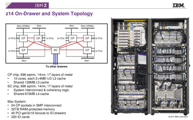
08:08PM EDT - Two clusters of CP chips connect to the SC. Can connect four drawers together
08:09PM EDT - CP and SC are large chips, 17 layer metal in 14nm SOI
08:09PM EDT - 10 cores has private 2MB L2-i and 4MB L2-D and 128 MB shared L3
08:09PM EDT - SC chip has 672MB of L4 and coherency logic
08:10PM EDT - Up to 24 sockets int he system, 32 TB RAIM protected memory, 40 PCIe lane fanouts, 320 IO cards
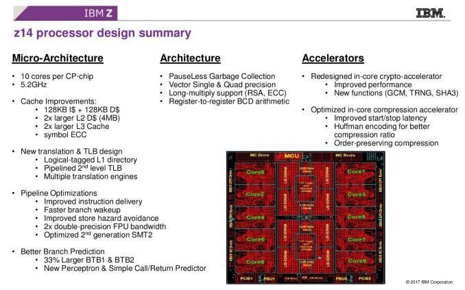
08:10PM EDT - New translation and TLB design over z13, and general pipeline optimations. Changes in instruction set too
08:10PM EDT - Pauseless garbage collection for Java, single and quad vector precision for crypto
08:11PM EDT - Register to register arithmatic
08:11PM EDT - Optimizing for COBOL performance (........)
08:11PM EDT - E.g. gazillions of lines of COBOL in online booking systems
08:11PM EDT - Compression acceleration
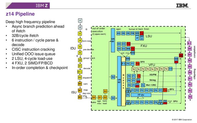
08:11PM EDT - This is the pipeline diagram
08:12PM EDT - 5.2 GHz, super long pipeline
08:12PM EDT - 6 instruction parse and decode, CISC instruction cracking
08:12PM EDT - 4-cycle load/use
08:12PM EDT - Directory and TLB pipeline changes
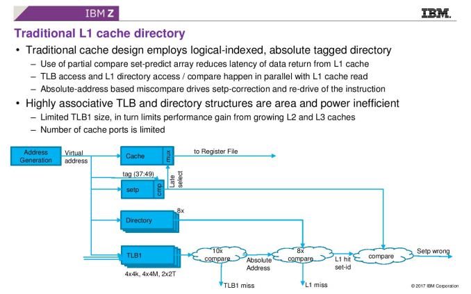
08:13PM EDT - Most designs use logical indexed, absolute tagged directory
08:13PM EDT - Use of partial compare set-predict array reduces latency of data return from L1 cache - TLB and L1 directory access happen in parallel with L1 cache read
08:13PM EDT - (doesn't that sound like way-prediction?)
08:14PM EDT - Highly associative TLB is area and power inefficiency, to limit TLB L1 size
08:14PM EDT - Sorry, I misread the slide, This is how L1 cache looks today
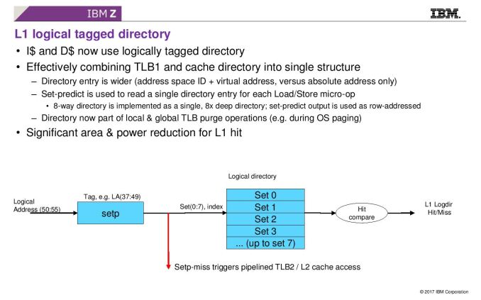
08:14PM EDT - This new slide shows how IBM is using it in z14
08:15PM EDT - I-cache and D-cache is now logically tagged, combining TLB1 and cache directory into single structure
08:15PM EDT - Significant area and power reduction for L1 hit
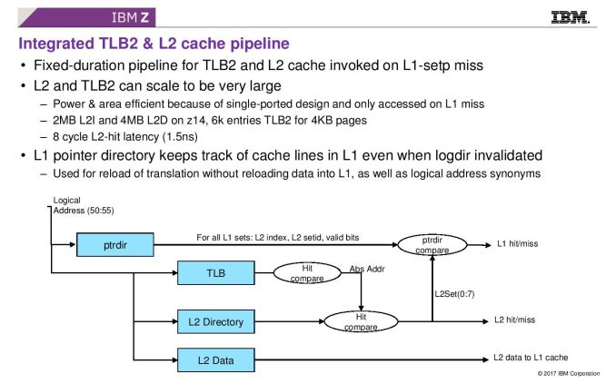
08:15PM EDT - Now a super large L2 TLB
08:16PM EDT - L2 and TLB2 can be large - 2MB L2I and 4MB L2D, 6k entries TLB2 for 4KB pages
08:16PM EDT - 8 cycle L2 hit latency (that's only 1.5 ns) ...
08:17PM EDT - Now crypto
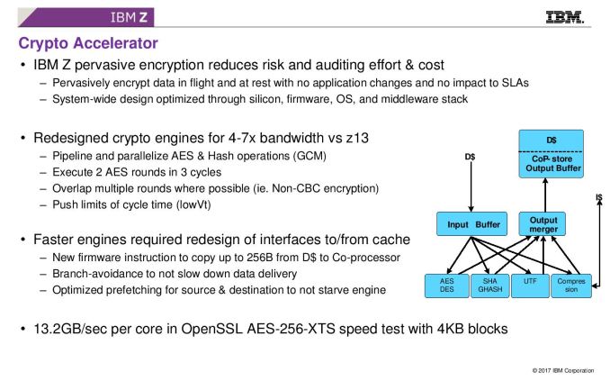
08:17PM EDT - Now redesigned for 4-7x bandwidth
08:17PM EDT - make it simple and fast enough to be able to encrypt all data
08:17PM EDT - combination of OS, firmware and hardware implementation
08:18PM EDT - Execute 2 AES in 3 cycles
08:18PM EDT - Copy up to 256B per instruction from D-cache to coprocessor
08:18PM EDT - can execute multiple AES at once, multiple engines on die
08:19PM EDT - 13.2GB/sec per core (so 132GB/s per CP, and about 1TB/s per 6-socket server)
08:19PM EDT - Use new instructions to feed crypto engine to avoid branches
08:19PM EDT - Avoid pipeline bubbles using new instructions
08:19PM EDT - Significant effort in prefetching as well
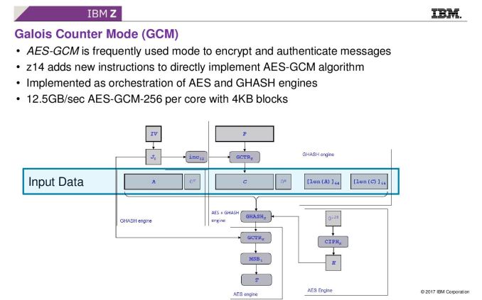
08:20PM EDT - New GCM instruction
08:20PM EDT - Algorithm that does encryption and signature authentication
08:20PM EDT - Implement use AES and GHASH engines
08:20PM EDT - the 2 engines used in concert rather than independently
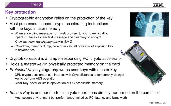
08:21PM EDT - Now key protection - most CPUs work with keys in memory. CryptoExpress6S is a tamper responding PCIe crypto accelerator. Master key is in physically protected memroy on card
08:21PM EDT - 'Clear Key Cryptography'
08:22PM EDT - Root key access usually means can steal key through mem access or core dump. This method means that the key is protected by tamper protection
08:23PM EDT - Secure Key is another mode, which diverts all crypto off the CPU onto the card instead
08:23PM EDT - This way the application never sees the key, just sees the encrypted data
08:24PM EDT - Creates a key token from the data, which remains in tamper resistent memory, and when data is decrypted, key is thrown away and new key generated
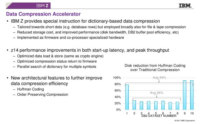
08:24PM EDT - Data Compression Accelerator
08:24PM EDT - Dictionary based data compression
08:25PM EDT - Reduces bandwidth need between memroy and disks, increases efficiency, implemented as irmware and co-processor specialized hardware
08:25PM EDT - *firmware
08:25PM EDT - z14 performance at peak throughput and start up latency. Optimized compression status return to firmware
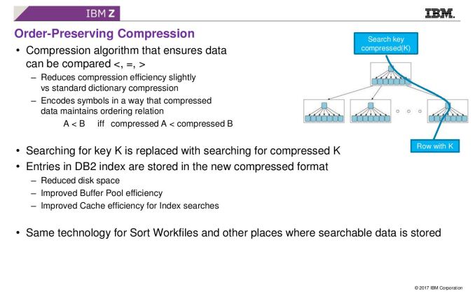
08:26PM EDT - Order-preserving compression: Allows data still be compared when compressed
08:26PM EDT - Allows compressed directory/tree structures to do comparisons between elements without decompression
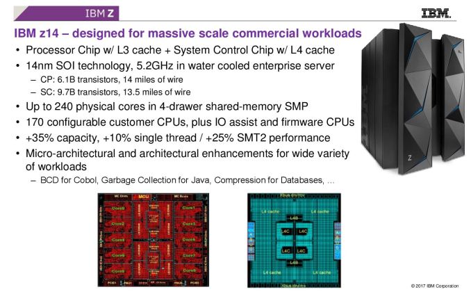
08:27PM EDT - CP has 7b transistors, SC has 10b transistors
08:27PM EDT - water cooled
08:28PM EDT - of 240 CPUs in a full system, 170 can be customer configured
08:28PM EDT - +35% capacity, +10 single thread, +25% SMT2 perf over z13
08:29PM EDT - Now for Q&A
08:29PM EDT - Q: Please generate workstations. I want to swap out x86 with z14
08:29PM EDT - (at same price, insert laughs)
08:29PM EDT - Not a serious question
08:30PM EDT - Q: What power for the chips?
08:31PM EDT - A: You can get the chips to run at any power you need. Could go 400-500W on high workload. We aim around 300-350W. We don't bin - there's only one product and we stay within the drawer power
08:31PM EDT - The chips themselves are water cooled, but customers can run an aircooled system, or you can hook up datacenter water
08:32PM EDT - Q: Doesn't going over the PCI card cause extra latency
08:32PM EDT - A: Card only has the master key - the data has a key token, which doesn't need to keep going back and forth
08:32PM EDT - Q: Have you considered something like SGX?
08:33PM EDT - A: That's not an apples to apples comparison. We consider the tamper resistant element a key feature of our products.
08:34PM EDT - Q: But SGX prevents someone with a logic analyzer going in
08:34PM EDT - A: Our solution does not need recoding - our customers use older software and it is transparent
08:34PM EDT - Q: What would you do to make COBOL run faster?
08:35PM EDT - A: COBOL does a lot of time doing BCD arithmetic, but there's traditional issue queue limitations, so we use packed BCD compute to reduce that bottleneck
08:36PM EDT - Q: What did +35% capacity and +25% SMT2 mean
08:37PM EDT - A: +35% is instructions for a whole system. The +10% single thread is a large scale number for benchmarks on capacity planning. +25% SMT2 from tuning and tweaking in our implementation due to maturity
08:37PM EDT - That seems to be a wrap. This is our last live blog on Hot Chips - I'll be writing up some of these talks on my flight home tomorrow. Hope you enjoyed them :)

