Original Link: https://www.anandtech.com/show/11737/analyzing-falkors-microarchitecture-a-deep-dive-into-qualcomms-centriq-2400-for-windows-server-and-linux
Analyzing Falkor’s Microarchitecture: A Deep Dive into Qualcomm’s Centriq 2400 for Windows Server and Linux
by Ian Cutress on August 20, 2017 11:00 AM EST- Posted in
- CPUs
- Qualcomm
- Enterprise
- SoCs
- Enterprise CPUs
- ARMv8
- Centriq
- Centriq 2400
Developing a custom microarchitecture is difficult. Even with all the standards in place and licensing an instruction set such as ARM, the actual development takes time and the right people to put together, then the infrastructure to deploy at scale.
In the mobile space, we’ve seen custom cores – most notably from Apple – deviating from the regular ARM design, but also Samsung and Qualcomm are playing in that space. Qualcomm however is going one further by developing a custom core for the server and enterprise market, focusing purely on typical enterprise workloads. The current commercial ARM success in the data center comes from companies such as Cavium, who use ARM architecture licenses in a custom SoC. By developing its own high-performance core, Qualcomm is hoping to offer something different in the data center, and they’ve lifted the lid on a good chunk of the core.
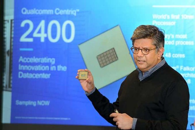
The Qualcomm Centriq 2400 SoC Family, with the Falkor CPU
Back in December 2016, Qualcomm announced that it has developed its own SoC for the data center, all the while also reveaing details such as the fact that it is a custom core and that Qualcomm will be involved in the Open Compute Project (and is based on the latest version of Microsoft’s Project Olympus). We knew that Qualcomm has been aiming for a 48 core design, using ARM’s instruction set, and is aiming for the data center and enterprise markets. The goal is to carry forward knowledge of the ARM instruction set and custom core design into markets that could potentially leverage it – it also helps that the data center market has a very interesting TAM (total addressable market, in USD) of which even a small slice could reap rewards. Back in December, they were beginning to sample cloud partners and potential future customers.
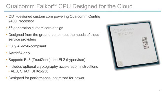
The first set of products to come out will be the Qualcomm Centriq 2400 family of SoCs. The top parts will feature 48 cores, and while today Qualcomm is ultimately communicating about said 48-core model, they have stated that the 2400-series will be a range of parts segregated by core count, performance, and power. The CPU cores, code named Falkor, will be ARMv8.0 compliant although with ARMv8.1 features, allowing software to potentially seamlessly transition from other ARM environments (or need a recompile). The Centriq 2400 family is set to be AArch64 only, without support for AArch32: Qualcomm states that this saves some power and die area, but that they primarily chose this route because the ecosystems they are targeting have already migrated to 64-bit. Qualcomm’s Chris Bergen, Senior Director of Product Management for the Centriq 2400, stated that the majority of new and upcoming companies have started off with 64-bit as their base in the data center, and not even considering 32-bit, which is a reason for the AArch64-only choice here.
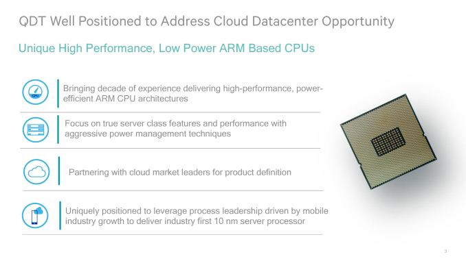
The design team behind the Centriq, as explained to us, was partly formed from the custom core team from the mobile side. On the mobile side we have seen Qualcomm custom cores based on ARM’s instruction set in the form of Krait and Kryo, although this new Falkor design is not derived from either. Qualcomm states that Falkor is their 5th generation of custom CPU core design, and has been a complete ground up design specifically for the data center. The focus, we were told, was on high overall performance, high performance per watt, but also the ability to run at low power. To do this, the Centriq 2400 is set to be the first major data center design built on a 10nm process.
We already know that it will be fabbed on a 10nm process, and various media/analysts have postulated which foundry will be playing that role. Qualcomm currently has 10nm volume with Samsung through the Snapdragon 835, which is shipping in the millions. Samsung’s 10nm processes are more mature than the competition at this point, however Samsung does not have much experience with large silicon dies, tending to favor smaller SoCs due to the naturally higher yields and helping to keep fab production at a high level. The other alternative is TSMC, whose CLN10FF process was technically available for select customer orders later than Samsung, but is currently being used by Apple's A10X in the iPad Pro 2. TSMC also has experience with larger silicon, which would be of considerable benefit. Qualcomm is not announcing who their foundry partner is at this time unfortunately, although it would likely depend on relations, volume, pricing and performance.
Enterprise Features: Security
With security being a strong focal point in data center tasks, all of the major players that want to provide processors for cloud deployments have been getting their hands dirty and talking security. The ability to provide security keys for hypervisors, VMs, and everything else that can be sandboxed from other users is paramount. To this extent, the Centriq 2400 is supporting two levels of security: EL3 and EL2. This means TrustZone at a system level (EL3) as well as a hypervisor level (EL2), although Qualcomm has not gone into detail if this extends through to having some VMs secure and others not within the same hypervisor environment. Where some of Qualcomm’s competitors are using ARM’s TrustZone implementation – which is an ARM Cortex-A5 for the management – Qualcomm has stated that their solution is not ARM based but a custom design that is TrustZone compliant. We confirmed that this wasn’t another re-use of an ARM architecture license.
Also for security, Qualcomm has added instructions geared towards cryptography acceleration, supporting AES, SHA1, and SHA2-256.
Enterprise Features: Secure Boot
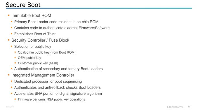
Implementing a Root of Trust has also being making the rounds in recent years. With nefarious code potentially rewriting firmware, or zero-day flaws in technology being exploited by friend and foe, being able to verify the underlying system is as intended and only as intended becomes paramount. Qualcomm’s Centriq 2400 will use Secure Boot functionality.
This is accomplished by providing an Immutable Boot ROM via an integrated management controller, with burned in code and cryptographic keys to authenticate firmware and software before any other firmware is loaded. Qualcomm states that this guarantees knowledge of ownership at the base level, as it allows customers to store (at purchase) public keys from Qualcomm, the OEM or the customer to authenticate secondary and tertiary bootloaders with an anti-rollback check. The management controller also supports accelerated cryptography on SHA for digital signatures and RSA public key operations.
Enterprise Features: QoS
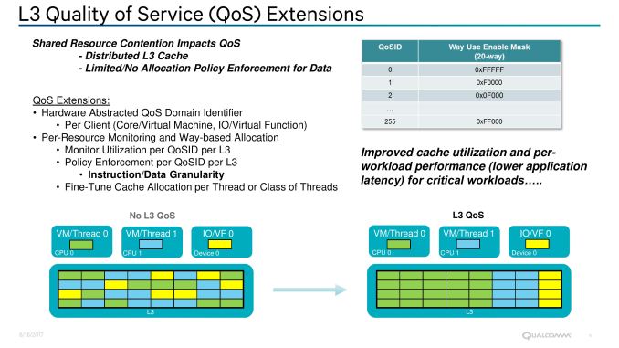
Also on the cards is L3 quality of service. In shared resource environments, mission critical applications can be disturbed by ‘noisy neighbors’. With multiple virtual machines vying for the same resources on a single machine, issues such as shared cache contention have flared up in recent quarters for data center use. If one VM is relying on consistent performance from memory accesses from cache but another program is thrashing it and causing inconsistent performance, the user experience can noticeably be disturbed.
There are multiple ways to tackle this, such as increasing the amount of private cache per core/VM, or by providing L3 cache Quality of Service (QoS) features. Intel has done both in recent years, such as increasing the amount of L2 private cache on the Skylake-SP Xeons from 256KB to 1MB, as well as offering L3 QoS since Broadwell-EP. AMD uses 512KB of L2 private cache, and also has QoS in play. Qualcomm isn’t disclosing the amount of L2 or L3 cache in today’s announcement, but were happy to discuss their QoS strategy.
Qualcomm has stated (despite some odd diagrams perhaps suggesting otherwise) that the L3 cache in the Centriq family is a distributed cache, which likely means that each core (or Duplex, more on that later) has a certain amount of associated L3 cache and L3 cache tags with it. By using a hardware abstracted QoS identification method per client, the SoC can monitor resources and enforce L3 QoS policies per domain ID and per L3 segment, down to the instruction and data level granularity. This is done using Way-based allocation, and policies can be adjusted or fine-tuned on the fly per thread or class of threads. Qualcomm’s implementation can support up to 256 defined environments, one of which can be designated or the SoC IO.
Enterprise Features: Memory Bandwidth Compression
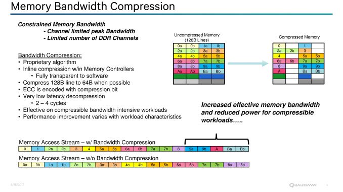
One of Qualcomm’s angles in the data center space is going to be that many data center workloads are memory bandwidth constrained. ‘Feeding the Beast’ is the limit for the markets they want to enter, so by enabling transparent memory compression out to DRAM, Qualcomm is attempting to address the issue. This feature will be transparent to any software, with the effect seen mostly in compressible data streams and memory streaming benchmarks.
By using a proprietary algorithm, Qualcomm’s inline compression will attempt to reduce a 128-byte cache line to 64-bytes with ECC as it moves into main memory. When recalling the data back into the core or for committing to storage, decompression adds an additional 2-4 cycles (1-2% on 250-cycle latency) but aims to bring more data in per request than uncompressed data. There could be a slight added benefit of lower power consumption as well, as less data is transferred. We’ve seen these techniques in the GPU space for a number of years.
From the software perspective, the effect will vary considerably from test to test depending on the workload. The Centiq 2400 series comes with six DDR4 memory channels, supporting two DIMMs per channel and up to DDR4-2667, so there’s going to be a lot of bandwidth to begin with – but sometimes that just isn’t enough.
The SoC: 48 Falcor Cores, DDR4, PCIe
Two decades ago, when processors were a single core with external memory controllers, external caches, and external IO, routing was comparatively easier than what we have today. Now we have many core systems, multiple cache levels of different varieties, more IO than we can shake a stick at, and it all has to communicate with each other in a low power, low latency and high bandwidth way using a variety of interfaces. For the Centriq 2400, Qualcomm is implementing a number of enterprise requirements as well as integrating its own developed fabric.
For those that have been following our Intel/AMD coverage of late, we discussed how internal coherent fabrics are changing: Intel has moved from a ring-bus topology to a per-core networking mesh, and AMD uses its scalable Infinity Fabric within a die, between dies, between sockets, and from GPUs to memory. In the mobile space, coherent fabrics like ARMs CCI/CCN are typically all the rage, and ARM allows its partners to modify and tune those IPs as they need to (and most do). Rather than using off-the-shelf IP, Qualcomm has stated that its new interconnect is homegrown.
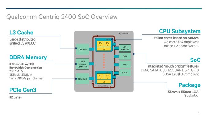
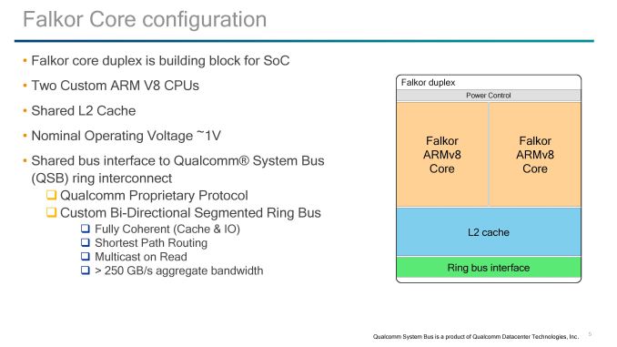
The Qualcomm System Bus (QSB) is a proprietary protocol based, bidirectional segmented ring bus. While Qualcomm shows a ring bus in the image above, we are told that the segmented ring bus might not exactly look like a ring inside the chip – by creating a segmented core-to-core design, it means the cores might not be in a ring at all, with some elements sprouting from off shoots and cores having more than one direction to travel. If Qualcomm were to share a false-color die shot, this would likely be visible. The QSB also allows for multicast on read as well as shortest path routing, which again sounds more like a mesh based networking implementation. Qualcomm quotes a >250GB/s aggregate bandwidth for the QSB.
On the Fabric is everything the system needs: cores, cache, memory, PCIe and IO.
The Centriq family will implement a pair of Falkor cores into a Falkor ‘Duplex’, where each core with have a private L1 cache and a shared L2 cache with ECC. We’ll cover the Falkor design in the next few pages.
For the L3 cache, Qualcomm has not quoted a size but has said that it will scale with the number of cores on the chip. In the above slide it states that it is a distributed unified cache, which can be confusing. Ultimately the cache is fully accessible from all cores, unless a QoS policy is in play, but the cache is likely segmented to allow for the relevant QoS policy tags to bind certain regions to certain cores/VMs. Despite it saying unified, it means that there will be partitions of the L3 around the QSB interconnect. The L3 will be with ECC as well.
Memory controllers are also accessed from the QSB interconnect, with the Centriq 2400 supporting six memory channels of up to DDR4-2667 at up to 2 DIMMs per channel. Support will include RDIMM and LRDIMM, which would suggest up to 1.5TB of LRDIMM support per socket using 128GB LRDIMMs, similar to Intel’s premium memory offerings.
Connectivity comes via 32 lanes of PCIe 3.0, which falls below that offered by Intel (32-44, fewer when chipset level Quick Assist or 10GbE is being used), AMD (128 PCIe in 1P or 2P), X-Gene 3 (42), or Cavium. We probed Qualcomm on features such as NVMe, NVMe RAID, and fall-over support, although in our limited time briefing there was not time to cover it – we might hear more while we are at Hot Chips this week.
Qualcomm has designed the chip as a true SoC such that it doesn’t need a chipset. We’ve confirmed that this is on-die connectivity, rather than via a multi-chip package add-in. The information we have states that the chip will support the usual array of SATA, USB, I2C, UART, GPIO and DMA, although how much of anything has not been stated.
The Duplex and Power Management
Like many processors on the market, design companies will use building blocks to assemble their complete processors. Equip those blocks with the right protocols, put them together, optimize, and create an advanced piece of sand that can decompress cat gifs if we prod it in the right way. Qualcomm’s main building block at the SoC level is the Falkor duplex, containing two Falkor cores, a shared L2 cache, QSB/fabric connectivity, and represents the lowest level of power management.
For SoC design followers, one might look at this design and think they see similarities with other dual-core designs such as AMD’s original Bulldozer design from 2011 or Intel's Xeon Phi. Internally, the cores are completely separate in terms of instruction throughput with no shared resources before the L2 cache. Consequently, between the two ends of the spectrum, Falkor is much closer to a Xeon Phi dual-core module, where each core has its own set of execution ports and vector extensions, but share an L2 cache and network connectivity.
But before diving into the cores, the L2 cache and power control require some explaining.
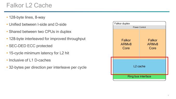
The L2 cache is a unified cache between both cores with ECC support, and inclusive of the L1-Data caches on both. Accesses are 128-byte interleaved with 128-byte lines, with 32-bytes per direction per interleave per cycle and 8-way associativity. ECC is using SEC-DED methodology, and the overall result as a minimum 15 cycle latency for an L2 hit, which is very competitive in the market. Qualcomm isn’t stating the size of the L2 cache at this time, which is somewhat of a surprise. In the market we see a variety of L2 cache options, so Qualcomm might end up offering a series of processors with different amounts of L2, especially if L2 defects are a factor in the manufacturing.
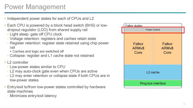
For power control, Qualcomm uses this unified design to control both cores. During our briefing we were told that both cores have to share the same frequency for L2 consistency; however the voltage per core can be adjusted and optimized for the best power implementation. As a result, power states between the cores can vary, and depending on the workflow needed, the cores and the L2 can also have different power states.
The cores in the duplex are powered by a block head switch or a low-dropout regulator (LDO), depending on the requirement. This allows for a variety of power down modes for the core logic, registers and caches:
- Light Sleep: CPU Clock is gated/lowered
- Voltage Retention: Registers and Caches retain state, logic is effectively off
- Register Retention: Registers retail state using main chip power rail, caches are off
- Collapse: Registers and L1 state not retained
The power control also maintains the state of the L2 cache, which offers modes similar to the CPU and may clock gate completely even with the CPUs in use. We confirmed that the L2 cache can only be on or off, and not in a half-use state.
Overall for power, Qualcomm is also implementing hardware state machines, to enable quick entry and exit to and from low power modes. Qualcomm explained that CPU use in data centers can be super low depending on time of day and requirements, so the ability to save power wake quickly was a fundamental design aspect for this chip, with the aim of reducing the electricity bill.
We know that these chips are built on a 10nm process, and when questioned Qualcomm stated that they will run above 2.0 GHz, while talking in about 1.0 V to do so while also being competitive in performance per watt. Unfortunately requests regarding TDP were returned with 'competitive for a data center environment'.
Getting Intimate with Falkor: The Front End
So we have to admit that we were surprised by Qualcomm releasing so much information about the pipeline. When we’ve ever asked the mobile CPU team about Krait and Kryo, we usually hit a brick wall, left with a PR answer of a ‘custom core design’ or the guide of ‘protecting our design’. So when Falkor was offered on a plate, we grabbed a knife and a chopstick to devour the soup at hand.
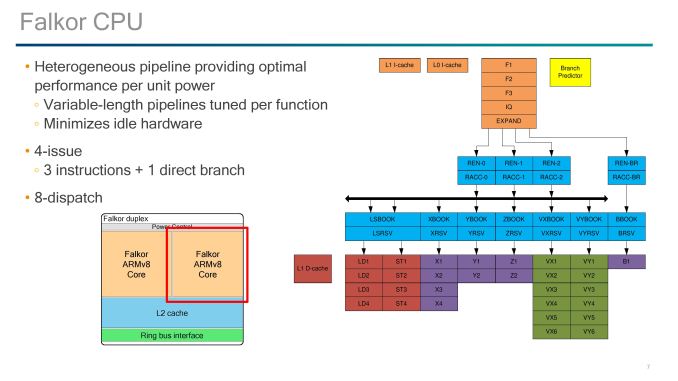
The headline features are as follows:
- Variable length pipelines, 10-15 stage depending on instruction
- 4-wide decode (3 + 1 branch)
- 8-wide out-of-order dispatch
- 8 execution ports
- Micro-op cache / L0 I-cache with Way prediction
- Retire 4/cycle usually (some situations >4)
Much like most modern cores and those built on ARM’s instruction sets, pipeline lengths vary for the different execution ports, and Qualcomm states that these are tuned depending on the instruction at play.
Just to add some terminology changes in here: what Intel calls a scheduler, ARM calls an Issue Queue, and Qualcomm calls a ‘Reserve’.
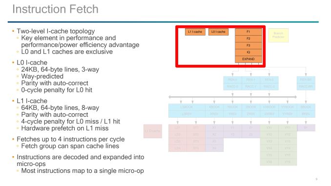
We start with a 4-stage instruction fetch, with the design able to fetch up to four instructions per cycle. These go into a single stage decode that converts the instructions into micro-ops, with most instructions becoming a single micro-op. Branches out of the decode are fed into their own branch rename stage and issue queue, before hitting its own execution port. Micro-ops not fed into the branch stage go into the single-stage rename and single-stage ‘register acccess’ followed by the out-of-order dispatch window.
Up to eight instructions can move into the two-stage Reserves/issue queues, with each execution port having one Reserve except for the load/store units which have a combined Reserve. Loads and stores take 4 stages, ALUs take 2 stages (most) or 4 stages (MUL), while FP and vector pipes take six stages.
For the fetch stages of the pipeline, Qualcomm doesn’t say much about its prefetch policies here. However we do have information about the branch predictor and L0/L1 caches.
The Front End: Prefetch and Branch Predictor
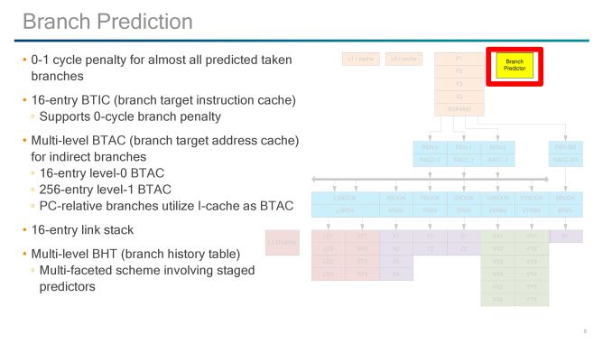
Qualcomm has implemented a custom branch predictor, and the design gives a 0-1 cycle latency penalty for taking most predicted branches. For instructions, there is a 16-entry branch target instruction cache (BTIC) that supports 0-cycle access, and for addresses there is a two-level branch target address cache (BTAC) for indirect branches: a 16-entry level 0 and a 256-entry level 1. This combines with the 16-entry link stack and multi-level branch history table for predictions.
The Front End: L0/L1 Instruction Caches
The instruction caches are an interesting part of the design, with Qualcomm implementing an L0 I-cache and an L1 I-cache. Qualcomm has implemented L0 caches before, since Krait, but when I initially saw it in this design I instantly thought it looks like a micro-op cache. (in LLVM commits it even states it as a micro-op cache). Normally the test is that if it walks like a micro-op cache and talks like a micro-op cache then it’s a micro-op cache, but the difference here is that rather than storing already-decoded micro-ops, it stores instructions ready to decode.
The special element to the L0 instruction cache here is that it is Way-predicted, meaning that the cache is checked for the instruction as the prefetch also checks the L1. As the L0 is smaller and closer to the event, it offers a 0-cycle latency for any instruction that achieves an L1 hit. The L0 sits at 24 KB, using 64-byte lines and 3-way associativity, but due to the way prediction, the L0 itself is transparent to software and will be seen as part of the L1 cache when metrics probe the size and capability.
The L1 I-cache is 64KB, which is similar to other ARM architecture core designs, and also uses 64-byte lines but with an 8-way associativity. To software, as the L0 is transparent, the L1 I-cache will show as an 88KB cache. Both the L0 and L1 have parity with auto-correct, and the L1-I has a four cycle penalty on an L0 miss. An L1 miss will initiate a hardware prefetch.
Instructions that go through the fetch end up in the decoders, with the Falkor design supporting 4-issue decode (3 decode + one branch).
The Front End: Rename, Register Access and Reserve (Rename and Dispatch)
It’s worth noting at this point that Qualcomm’s slides seem to make instructions and micro-ops interchangeable at this point, or rather use the term ‘instruction’ where they mean ‘micro-op’.
Direct branches out of the decoder hit their own rename and dispatch pipeline and execution, so the main focus is on the three other decoded micro-ops. Each of these hits the rename and completion buffer, which can support up to 256-entries.
The Qualcomm diagram gets a bit odd here as after the rename/register access stages, the micro-ops hit the out-of-order dispatch buffer. This supports 76 committed micro-ops ready for dispatch or retirement while 128 uncommitted micro-ops can remain in flight, although Qualcomm doesn’t state if these numbers include the Direct Branch decode (it’s worth noting that A73/A75 do not, but A53 does).
The dispatch buffer can push through eight micro-ops per cycle into the reserve stations/issue queues, although only one reserve will serve each execution port, much like a Cortex-A75 design. This means that in order to dispatch eight per cycle, it needs one of each of the execution ports in play. The exceptions to the rule are the two load/store units that use a combined reserve station.
Getting Intimate with Falkor: The Back End
The meat and potatoes of Getting Things Done™ is in the core logic – processing instructions with the right data to get the output. The Falkor design has eight of these execution ports: two for load/data, three for ALU/INT, two for FP/vector extensions, and one for direct branches.
The Back End: Load/Store and the L1-Data Cache
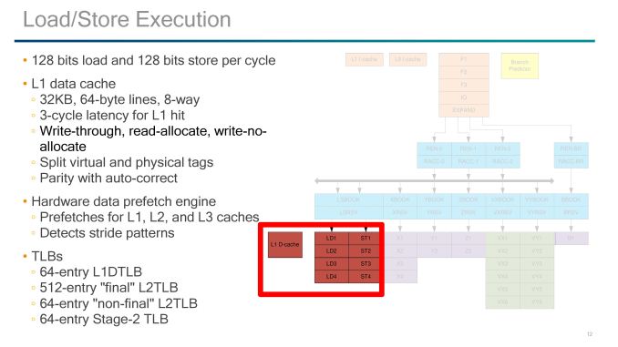
The load and store units are usually some of the most vital elements to the design, and here Qualcomm implements 1x128-bit Load and 1x128-bit Store per cycle. Unlike some other competitor designs, there is one unit specifically for load and one specifically for store, rather than issuing two of the same per cycle. These two units have a 3-cycle latency to a hit in the L1-Data cache, which is one cycle faster than most of the competition.
In order to get the latency low, the L1-D cache has to be designed appropriately. So here is a 32KB 8-way design, supporting 64-byte lines but also implementing a write-through strategy. This means that any data committed to L1-D will also be written to the L2. Hardened veterans may recall that the write-through policy was a sizeable bottleneck on AMD’s early Bulldozer designs, so the hope here is that Qualcomm won’t fall into the same trap. The L1-D also supports read-allocate and write-no-allocate modes with split virtual and physical tag addressing.
If a miss occurs on the L1-data cache, hardware data prefetchers are used to probe the L2 and L3 caches. Mechanisms are in place to also detect stride pattern access and compensate accordingly. There are two levels of data TLB in place, although as written it comes across as a four-level TLB. It starts with a 64-entry level 1 DTLB, then a larger 512-entry level 2 ‘final’ DTLB. This is backed by a 64-entry level 2 ‘non-final’ DTLB and another 64-entry ‘stage 2’ TLB.
The Back End: ALUs, Vector Extensions, and Branches
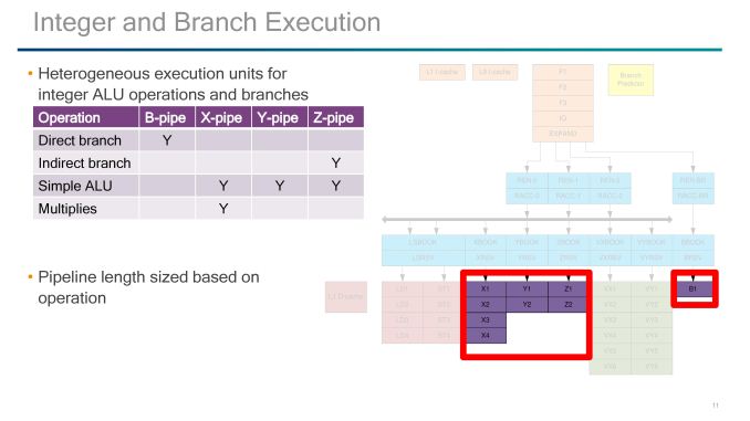
On the simple ALU side of the execution ports, Qualcomm labels theses as B, X, Y, and Z-pipes, with a mixed functionality between them and they have different pipeline lengths based on which pipe is needed.
B is for the Branch Pipe, which is for direct branches through the branch side of the decode/rename/queue of the back-end.
The XYZ pipes all perform simple ALU tasks, however only the X pipe can perform MUL operations and takes four stages, and the Z-pipe is the only one for indirect branches. The Y is a simpler ALU-only pipe, with the Y and Z pipe both taking two stages.
The pipes that Qualcomm did not talk about are the VX and VY pipes, which both come in at six stages each. V in this case likely stands for vectors, and may represent traditional NEON/FP operations found in the smartphone cores in mobile or perhaps the new Vector Extensions (VX?) which ARM introduced last year but have so far not been announced in any commercial product. Vector Extensions would allow for 128-2048 bit wide FP compute, and the idea is that the code required for implementing the vector extensions should be agnostic to how big the vector units actually are. Under ARM’s description, the pipeline should be able to process the data appropriately (although this has a knock on effects for latency if not configured for the ideal vector width).
Closing Thoughts: Qualcomm’s Competition
For the most part, five/six major names in this space are competing for the bulk of data center business: Intel, AMD, IBM, Cavium, and now Qualcomm. The first two are based in the omnipresent x86 architecture and are using different microarchitecture designs to account for most of the market (and Intel is most of that).
Intel’s main product is the Xeon Scalable Processor Family, launched in July, and builds on a new version of their 6th Generation core design by increasing the L2 cache, adding support for AVX-512, moving to an internal mesh topology, and offering up to 28 cores with 768 GB/DRAM per socket (up to 1.5TB with special models). Omnipath versions are also available, and the chipset ecosystem can add support for 10 gigabit Ethernet natively, at the expense of PCIe lanes. Xeon systems can be designed with up to 8 sockets natively, depending on the processor used (and cost). Interested customers can buy these parts today from OEMs.
Intel also has the latest generation of Atom cores, found in the new Denverton products. While Intel doesn’t necessarily promote these cores for the data center, some OEMs such as HP have developed ‘Moonshot’ style of deployments that place up to 60 SoCs with up to 8 cores each in a single server (which can move up to 16 cores per SoC with Denverton).
- Intel Unveils the Xeon Scalable Processor Family: Skylake-SP in Bronze, Silver, Gold and Platinum
- Intel's Skylake-SP Xeon versus AMD's EPYC 7000 - The Server CPU Battle of the Decade
AMD meanwhile launched their attack back on the high-end server market earlier this year with EPYC. This product uses their new high-performance Zen microarchitecture, and implements a multi-silicon die design to supports up to 32 cores and 2 TB of DRAM per socket. By implementing their new Infinity Fabric technology, AMD is promoting a wide bandwidth product that despite the multi-silicon design is engineered with strong FP units and plenty of memory and IO bandwidth. Each EPYC processor offers 128 PCIe lanes for add-in cards or storage, and can use 64 PCIe lanes to connect to a second socket, offering 64 cores/128 threads with 4TB of DRAM and 128 PCIe lanes in a 2P system. AMD is slowly rolling out EPYC to premium customers first, with wider availability during the second half of 2017.
IBM is perhaps the odd-one out here, but due to the size is hard to ignore. IBM’s POWER architecture, and subsequent POWER8 and upcoming POWER9 designs, aim heavily on the ‘more of everything’ approach. More cores, wider cores, more threads per core, more frequency, and more memory, which translates to more cost and more energy. IBM’s partners can have custom designs of the microarchitecture implementation depending on their needs, as IBM tends to focus on the more mission critical mainframe infrastructure, but is slowly attempting to move into the traditional data center market. Large numbers such as ‘5.2 GHz’ can be enough to cause potential customers do a double take and analyze what IBM has to offer. We’ve tested IBM’s base POWER8 in the lab, and POWER9 is just around the corner.
- Assessing IBM's POWER8, Part 1: A Low Level Look at Little Endian
- Assessing IBM's POWER8, Part 2: Server Applications on OpenPOWER
Cavium is the most notable public player using ARM designs in commercial systems so far (there are a number of non-public players focusing on niche scenarios, or whom have little exposure outside of China). The original design, the Cavium ThunderX, uses a custom ARMv8 core, and is designed to provide large numbers of small CPU cores with as much memory bandwidth and IO as possible. For a design that uses relatively simple 2 instruction-per-clock CPU cores, the ThunderX chips are quite large, and Cavium is positioning that product in the high performance networking market as well as environments where core counts matter than peak performance, as seen in our review which pegged per-core performance at the level of Intel’s Atom chips. The newer ThunderX2 is aiming at HPC workloads, so it will focus more on higher per-core performance. With ARM having recently announced the A75 and A55 cores under the DynamIQ banner, we’re expecting Cavium’s future designs to use a number of new design choices.
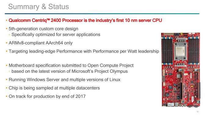
So now Qualcomm enters the fray with the Centriq 2400 family, using Falkor cores, aiming to go above Cavium and push into the traditional x86 and data center arena where others have tried and got stuck into a bit of a quagmire. Qualcomm is hoping that its expertise within the ARM ecosystem, as well as the clout of the new product, will be something that the Big Seven Plus One cannot ignore. One big hurdle is that this space is traditionally x86, so moving to ARM requires potential code changes and recompiling that will lose potential software efficiency developed over a decade. Also the Windows Server market, which Qualcomm is solving with Microsoft with a form of x86 emulation. Much like we have been hearing about Windows 10 on Qualcomm’s Snapdragon 835 mobile chipsets, Qualcomm is going to be supporting Windows Server on Centriq 2400-series SoCs.
Wrapping thigns up, while Qualcomm has given us more information than we expected, we’d still love to hear exact numbers for L2 and L3 cache sizes, die sizes, TDPs, frequencies (we’ve been told >2.0 GHz with no turbo modes), the different SKUs coming to market, and confirmation about which foundry partner they are using. Qualcomm will also have to be wary about ensuring sufficient support on all operating systems for customers that are interested, especially if this hardware migrates out of the specific customer set that are amenable to testing new platforms.
The Centriq 2400 family is currently being sampled in data centers, and moving into production by the end of 2017. The media sample timeframe unknown, however we're hoping we can get one in for testing before too long.

