Original Link: https://www.anandtech.com/show/1160
Gigabyte 8S655FX Ultra (SiS 655FX): Price/Performance Reaches a New Level
by Evan Lieb on September 22, 2003 12:13 AM EST- Posted in
- Motherboards
Weeks ago, SiS introduced their SiS 655FX chipset to a rather uninterested crowd of enthusiasts who were already immersed with the latest 865PE and 875P motherboards. Understandably so, motherboard makers haven’t been too keen on the SiS 655FX because of Intel’s great success with the 865PE and 875P chipsets in the enthusiast market (though, Intel obviously didn’t have any competitors, until now that is).
However, if there’s one thing SiS has always been good at, it’s been introducing products with great price/performance. The SiS 655FX chipset, thankfully, is no different. The Gigabyte 8S655FX Ultra is absolutely packed to the brim with onboard features, making it a high-end motherboard. But one characteristic that the 8S655FX Ultra doesn’t carry as a high-end motherboard is a high price; the 8S655FX Ultra’s retail price rivals that of low-end value motherboards, such as the ABIT IS7-E and IS7.
Read on to find out why you will love, and why you may even hate, this high-end motherboard with a value level price tag.
First Look at SiS 655FX Chipset
Before we get to Gigabyte’s 8S655FX Ultra motherboard, we’d like to take a quick look at the SiS 655FX chipset itself, seeing as how this is our first review of a retail motherboard based on this chipset. Let’s get right to it.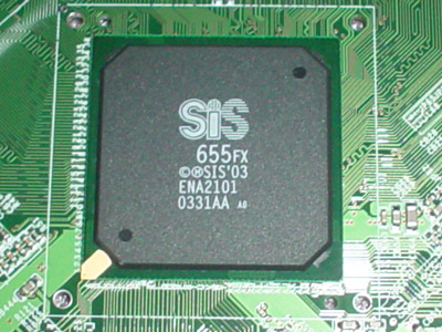
The SiS 655FX North Bridge itself differs from SiS’ previous flagship Pentium 4 North Bridge, the SiS 655, in one significant way — a revamped memory controller capable of operating at dual DDR400 memory speeds. In other words, the SiS 655FX, like Intel’s 875P chipset, is a dual channel DDR chipset that is capable of offering a total memory bandwidth of 6.4 GB/s.
Of course, what good would a memory bandwidth of 6.4 GB/s do if the FSB (Front Side Bus) wasn’t operating at a speed that could take advantage of that bandwidth? Well, this is exactly where the second and final most significant difference between the 655FX and 655 comes into play — support for 800MHz FSB Pentium 4 processors, otherwise known as Northwood “C” series of processors (such as Intel’s flagship 3.2C processor).
While the SiS 655 North Bridge did indeed support Intel’s Hyper-Threading (HT) technology, it was only able to do so with a second spin of that North Bridge, the B0 revision. For a while, retail motherboards were shipping with early stepping SiS 655 North Bridges (an “A” series stepping of some sort) that could not support Intel HT. Some motherboards (Gigabyte’s, in particular) were able to support HT with “A” stepping North Bridges, but it entailed a BIOS update that involved turning off power related features that normally wouldn’t be advisable for overclockers and other such performance users (like ACPI). So, with the SiS 655FX, you won’t have to worry about HT support, because all 655FX will support HT no matter what.
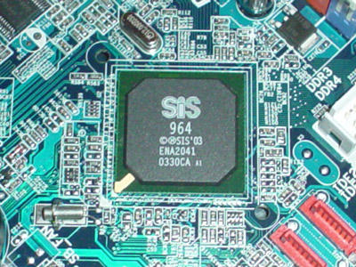
The SiS 964 is just the third South Bridge in the world shipping with native Serial ATA support. The SiS 964 supports two independent Serial ATA connectors with support for RAID 0 and RAID 1. Unfortunately, it looks as if RAID 0 + 1 isn’t possible for now, though we’ll have to confirm details about a supposed SiS 964 revision that adds some very interesting features, including RAID 0 + 1 array capability among other things.
A second unique feature that is less interesting, but new nonetheless, is the support for two additional USB 2.0 compliant ports. Previously, the SiS 963 South Bridge supported just six total USB 2.0, as did Intel’s South Bridges before the ICH5 and VIA’s South Bridges before the VT8237. Luckily, SiS followed suit and supports a total of eight USB 2.0 ports, just as the VT8237 and ICH5. Eight USB 2.0 ports should truly be enough for the overwhelming majority of computer users, especially since IEEE 1394 FireWire 400 capability is integrated on many high-end desktop motherboards (like the Gigabyte 8S655FX Ultra) or can be purchased and installed as a PCI device.
Everything else about the SiS 964 is identical in nature to the SiS 963 that so many motherboards before it were based on, such as the 1GB/s MuTIOL I/O link and AC’97 V2.3 compliant audio controller, among other basic features.
Gigabyte 8S655FX Ultra Rev. 1.0: Basic Features
| Motherboard Specifications | |
| CPU Interface | Socket-478 |
| Chipset | SiS 655FX North Bridge SiS 964 South Bridge |
| Bus Speeds | up to 355MHz (in 1MHz increments) |
| Core Voltage | up to 1.600V (in 0.0125V increments) |
| DRAM Voltage | up to 2.60V (in 0.1V increments) |
| Chipset Voltage | N/A |
| AGP Voltage | up to 1.80V (in 0.1V increments) |
| Memory Slots | 4 X 184-pin DDR DIMM Slots |
| Expansion Slots | 1 X AGP 8X Slot 5 X PCI Slots |
| Onboard IDE RAID | ITE GigaRAID IT8212F controller |
| Onboard USB 2.0/IEEE-1394 | Eight USB 2.0 ports supported by SiS 964 South Bridge TI TSB43AB23 IEEE 1394 FireWire (up to 3 ports) |
| Onboard LAN | Realtek RTL8169 10/100/1000 Gigabit adapter |
| Onboard Audio | Realtek ALC658 AC’97 codec |
| Onboard Serial ATA | Two SATA connectors via SiS 964 (RAID 0 & RAID 1) |
| BIOS Revision | F1 (August 18th, 2003) |
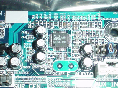
Gigabyte uses a Realtek ALC658 AC’97 Codec for sound processing onboard the 8S655FX Ultra. This is the first motherboard that we’ve seen with this brand new Realtek Codec, but this isn’t at all surprising considering Gigabyte was the first to ship a desktop motherboard with the Realtek ALC655 AC’97 Codec. Anyway, the ALC658 AC’97 Codec is actually a Professional-level Codec and not a mainstream-level Codec like the ALC655. The primary difference between these two Codecs is that the ALC658 has six 20-bit DAC channels, whereas the ALC655 contains just one 16-bit DAC channel. Basically, the ALC658 will output higher quality sound than a similarly equipped ALC655-based motherboard.
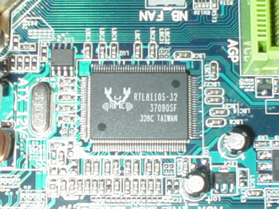
The 8S655FX Ultra utilizes Realtek’s latest Gigabit controller, dubbed the RTL8169. This IC, like any other Gigabit device, is capable of supporting 10/100/1000 transfer rates. There’s nothing especially unique about this Gigabit controller, though we’re certainly happy that Gigabyte decided to add on a Gigabit controller to their 8S655FX Ultra, as this standard needs to be pushed aggressively for full support to come as soon as possible to take full advantage of it. Unfortunately, SiS did not develop its own proprietary GbE (Gigabit Ethernet) bus separate from the PCI bus. Intel was able to do this with their CSA (Communications and Streaming Architecture) GbE technology (we proved this back in April), which is much more effective than transferring data via the 133 MB/s constrained PCI bus.
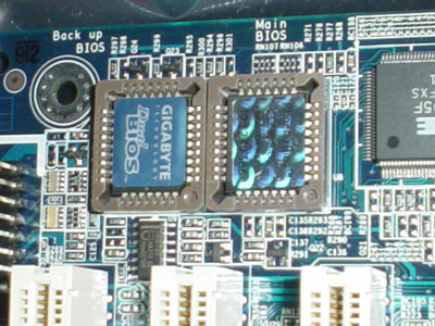
Common among Gigabyte’s high-end motherboards, the 8S655FX Ultra includes dual BIOS technology. Having a backup BIOS is beneficial when you accidentally corrupt your first BIOS chip (i.e. you lose power to your system as you're updating your primary BIOS). Simply switch over to the second BIOS chip, and your machine becomes operational once again, and your original BIOS settings originating from the first chip are even mirrored to the second chip. This feature gets rid of all the frustration and inconvenience of correcting the problem through other, time-consuming methods, such as a full board RMA or the swap-trick.
Gigabyte includes a nice array of I/O ports onboard the 8S655FX Ultra. These I/O ports include two PS/2 ports, one parallel port, two serial ports, four USB 2.0 ports, one GbE 10/100/1000 port, and Mic in, Line in, and Line out, which drives the onboard sound. We’re pleased to see more than just two rear USB 2.0 ports, especially since there are many more convenient reasons to use USB devices today with the advent of such innovative technologies as USB memory keys. Thankfully, there are two onboard USB 2.0 headers if you feel the need to expand beyond four USB 2.0 ports. Unfortunately, you’ll have to use up two PCI slots, but this may likely not be an issue considering the sheer amount of onboard components the 8S655FX Ultra carries. Still, if you feel the need to add on something like a modem, a better RAID controller, or any other such PCI devices, you’ll have three PCI slots available with the other two PCI slots occupied by two 2-port USB 2.0 headers.
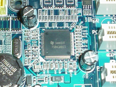
Texas Instruments has been doing quite well with their IEEE 1394 FireWire controllers, and the 8S655FX Ultra is no exception. The onboard FireWire controller is powered by the TI TSB43AB23, which supports a total of three FireWire ports. We’re disappointed that Gigabyte didn’t throw in at least one rear FireWire port. After all, it does take extra time out of the day to install that FireWire bracket. Still, FireWire is FireWire, and it’s always good to see an alternative to USB, especially if you’re a heavy DV camera user. Hopefully, we’ll see a future SiS South Bridge with native support for IEEE 1394 FireWire 400 so that DV camera users can take advantage of that 1GB/s I/O link.
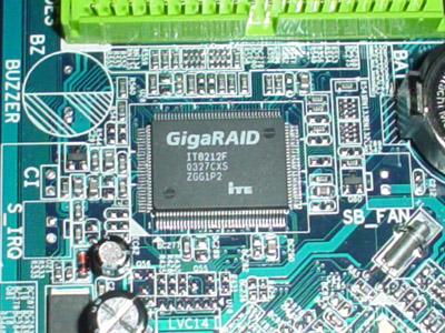
One of the most notable features the 8S655FX Ultra carries is onboard IDE RAID from ITE, named the GigaRAID IT8212F controller. There are two onboard IDE connectors that are powered by the GigaRAID IT8212F controller, which is capable of RAID 0 (striping), RAID 1 (mirroring) and RAID 0 + 1 RAID arrays. Not only can this controller support a total of four HDDs (hard disk drives), but four ATAPI (optical) drives as well. This is a considerable advantage over other motherboards with Promise or Silicon Image controllers that are only capable of supporting HDDs.
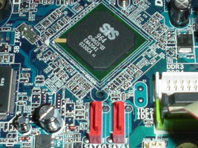
The final significant onboard feature that the 8S655FX Ultra carries is native SATA support courtesy of the SiS 964 South Bridge. The two SiS 964-controlled SATA connectors use the 1GB/s MuTIOL I/O link for data transfer, so you aren’t bound to the 133MB/s PCI bus. This will free up your PCI bus and improve your SATA slightly (though the difference is minuscule knowing that most apps can hardly use all that bandwidth). Both these SATA connectors are SATA150 compatible. Skip back to the “First Look at SiS 655FX Chipset” for more details about this feature.
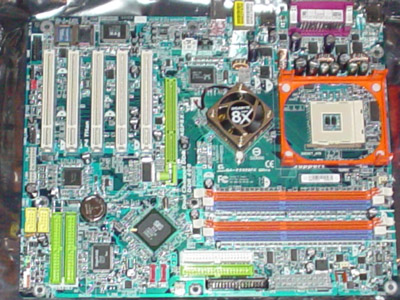
Gigabyte 8S655FX Ultra: Board Layout
Gigabyte does a fine job of laying out yet another motherboard. The 8S655FX Ultra has a nearly flawless components layout.
The 8S655FX Ultra’s ATX connector is placed on the right-hand side of the motherboard, just over an inch below the top right-hand corner of the PCB. This is just about the ideal location for the ATX connector due to the fact that standard PSUs often do not have an extra long ATX cable, which would normally cause an increase in clutter and obstruction of the installation/uninstallation of the CPU HSF, memory modules, or other components with a poor ATX connector placement. However, the 8S655FX Ultra’s ATX is placed where it should be and so this is not a problem. However, since the 8S655FX Ultra is a high-end motherboard, most users aren’t going to think twice about a no-name PSU and will instead opt for a high-quality PSU with an extra-long ATX connector.
As usual, Gigabyte places their Primary and Secondary IDE connectors in the absolute ideal locations above the midsection of the motherboard on the right-hand corner of the PCB. This location is good because it allows the 8S655FX Ultra’s bundled IDE cables to reach the first and second bays of a full sized ATX computer case. Normally, with the Primary and Secondary connectors located below the midsection of the motherboard, it would be almost impossible to route a standard pair of IDE cables high enough to reach the first drive bay, and perhaps even the second bay. For enthusiasts who are fanatical about case organization, this layout design choice is an absolute must for any modern day desktop motherboard.
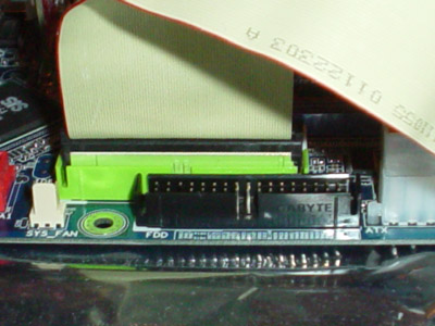
You wouldn’t normally hear us say that having the Floppy connector high up on the right-hand side of the motherboard is a good location, but in the 8S655FX Ultra’s case, it’s actually not too bad of a situation. In this situation, the Serial ATA connectors and IDE RAID connectors onboard the 8S655FX Ultra are located well enough below the Floppy connector that the Floppy cable won’t collide or cause any other organizational havoc. And because the Floppy connector is placed directly to the right of the Primary and Secondary connectors, the Floppy cable and IDE cables won’t cross paths. Gigabyte nicely avoids a potential nightmare for neat freaks out there.
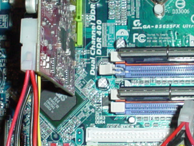
One of the best layout decisions a motherboard maker can make is the placement of the DIMM connectors. The 8S655FX Ultra’s DIMM connectors are positioned far enough away from the AGP slot (the video card) that end users will have no worries about swapping out or upgrading memory modules in the future. You see, normally, if the DIMM connectors were located so close to the AGP slot that they could not be fully opened with a video card installed, the user would be forced to go through the painstaking process of unscrewing the video cards primary screw, physically uninstalling the video card from its AGP slot (not to mention any 4-pin connectors or other connectors depending on the video card) and unscrewing the VGA monitor cable just to have access to the memory slots. Clearly, it would be much easier if a motherboard maker were just to locate the DIMM connectors far enough away from the AGP slot so that this does not become a problem. Thankfully, Gigabyte is one of these motherboard makers, and given their past execution on the board layout front, we’re not surprised that they continue to excel at this area of desktop motherboard design.
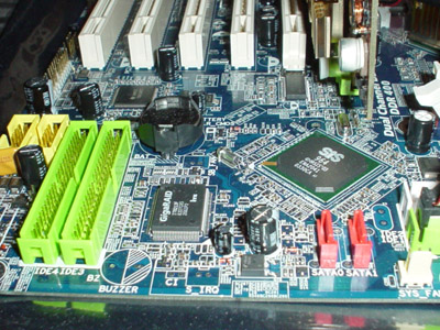
The final excellent layout choice Gigabyte’s engineers made with the 8S655FX Ultra is the placement of the ITE GigaRAID IDE connectors and SiS 964 Serial ATA connectors. The IDE RAID connectors’ location is excellent because they are placed at the bottom of the motherboard where a good computer case will have several HDD (hard drive disk) bays for a RAID array to be constructed. The Serial ATA connectors’ location is equally good for the same reason — near the bottom of the board (though, admittedly, a bit too high) where they can be cleanly routed to their respective SATA drives.
Gigabyte 8S655FX Ultra: BIOS and Overclocking
Gigabyte continues to use an Award BIOS for their desktop motherboards. Luckily for Gigabyte, they’ve been one of the few manufacturers to encounter very few BIOS-related performance issues with their desktop motherboards, and this is worth commendation given the rather inconsistent early BIOS performance issues that plague many other manufacturers’ BIOSes.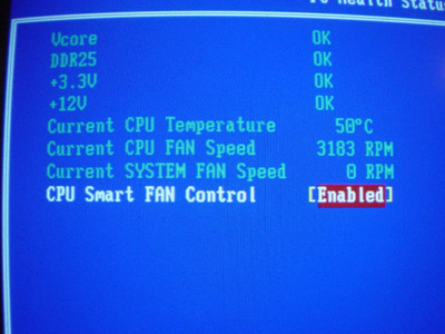
Looking at Gigabyte’s PC Health section within the 8S655FX Ultra BIOS, we see that Gigabyte is continuing the unfortunate trend of using an “OK” in place of an actual reading for many of the vital options that many users like to know about in their system. For example, Vcore, VDIMM, and the 3V and 12V PSU rails are given an “OK” instead of a reading voltage value. This is simply unacceptable for enthusiasts, as most of these types of users prefer to have some understanding of how their voltages are fluctuating. An “OK” is simply too vague. The one vital reading shown in this section is CPU temperature, which reads 50C running at 3.0GHz at 800MHz FSB, spot on. The only other readings left in the PC Health section are CPU and System fan speed readings. One nice touch to this BIOS is the addition of a “CPU Smart Fan Control” option in the PC Health section. PC noise is a big deal nowadays, so options like this one are important. Still, this option is limited in nature, and the rest of the 8S655FX Ultra’s PC Health is simply too incomplete. Hopefully, Gigabyte will improve in this area.
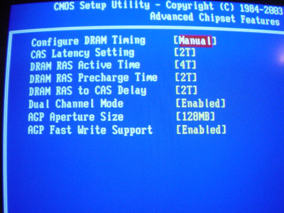
The 8S655FX Ultra’s Advanced Chipset Features section is hidden. This is a common feature among Gigabyte motherboard BIOSes, because Gigabyte feels that it’s in the best interest of its customers that they not play with settings with which they are unfamiliar. We agree to a point, but still think it’s unnecessary to hide this section. Anyway, the 8S655FX Ultra’s Advanced Chipset Features section includes memory timing settings such as CAS Latency, RAS Precharge, RAS to CAS Delay, and Precharge Delay. By default, dual channel DDR mode is enabled if you install one memory module into DIMM’s number one and three in your motherboard. An option called “Dual Channel Mode” is available in this section that can be set to enabled or disabled; obviously, you should keep it enabled. The final two available options in this section are AGP Aperture Size (which was set to 128MB for our 9800 Pro benchmark tests) and AGP Fast Write support. Thankfully, loading the “Optimized Defaults” in the 8S655FX Ultra’s BIOS keeps fast writes enabled. If you are experiencing reliability issues with your system, however, there is a possibility that enabling fast writes could be causing the problem. ATI 9700 Pro video cards were notorious for having odd issues with AGP 8X and fast writes with certain motherboards, so be wary if you’re a 9700 pro owner. We haven’t experienced this issue with the 9800 Pro on any of the motherboards that we’ve tested in the last two months though, and our sources tell us that this isn’t an issue anymore, so we’re fairly confident that everything has been resolved.
|
Click to enlarge. |
Click to enlarge. |


In the Frequency/Voltage Control section, the 8S655FX Ultra offers a huge range of DRAM selection. When the FSB is set to 200MHz (or 800MHz quad pumped), you end up with DRAM frequency options such as 400MHz, 606MHz, 362MHz, 538MHz, 672MHz, 504MHz, 484MHz, and 454MHz, among other lower frequencies. This is an extremely impressive range of DRAM options, probably the most varied array of DRAM settings that we’ve ever seen from an Intel motherboard.
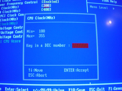
True to tradition, Gigabyte includes FSB adjustments well in excess of what any overclocker will be able to achieve. The 8S655FX Ultra BIOS allows up to 355MHz FSB, which even hardcore overclockers will never be able to reach. This will allow the sort of performance and tweaking ability that enthusiasts enjoy.
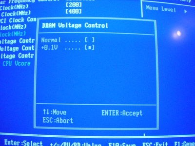
The Gigabyte 8S655FX Ultra’s “weakest link” in terms of BIOS options is most definitely its lack of wide VDIMM control. VDIMM is available up to a paltry 2.6V. As Wesley Fink proved in his Holy Grail Memory articles (Part 1 and Part 2), high speed memory modules can run well at lower voltages, but that higher than 2.6V is needed for stable DDR500 operation and higher. Because the Pentium 4’s FSB bandwidth is so large at overclocked FSB speeds (between 1000MHz FSB and 1200MHz FSB mostly), having too low a VDIMM BIOS option will hinder the amount of bandwidth that your memory modules can feed to your system. Therefore, 2.6V is unacceptable. High-speed memory (such as PC3700, PC4000, and PC4200 modules) absolutely need more voltage, as we proved in our Holy Grail series of Memory articles.
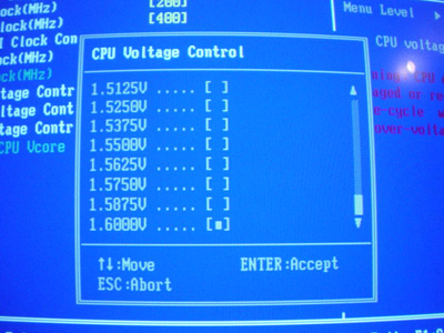
If the 8S655FX Ultra’s “weakest link” in terms of BIOS options is its lack of wide VDIMM control, then second in line for the “weakest link” would be its lack of varied Vcore control. The 8S655FX Ultra BIOS, unfortunately, only allows up to 1.60V in 0.0125V increments. While this won’t limit your stable FSB overclock too much, it will limit the absolute potential of this motherboard. Therefore, hardcore overclockers will definitely be disappointed with the 8S655FX Ultra and will stray far away from it. However, since low-end P4 processors such as the 2.4C are usually such spectacular overclockers on default Vcore (1.525V), 1.60V should be more than enough for even serious (but not hardcore) overclockers. We must warn you that the 8S655FX Ultra may be undervolting Vcore a bit, but we can’t know for sure since the 8S655FX Ultra’s PC Health section did not list any Vcore readings.
The 8S655FX Ultra’s VAGP options range from 1.5V to 1.8V in 0.1V increments. Video card overclocking enthusiasts will be more than pleased with this voltage range, as anything over 1.6V really isn’t necessary the vast majority of the time.
In what is certainly a positive sign for enthusiasts looking to entrust their overclocking hopes on a SiS 655FX motherboard, the 8S655FX Ultra BIOS has an AGP/PCI lock. The PCI adjusts accordingly to what the AGP bus is set; for example, a 66MHz AGP bus speed would obviously yield a 33MHz PCI bus speed. However, a 70MHz AGP bus speed would yield a 35MHz PCI bus speed, not 33MHz. This is the only unfortunate side affect of not having a truly locked PCI bus, but during FSB overclocking, the AGP and PCI buses are definitely locked at their respective default speeds, that much is certain (and a boon for overclockers everywhere).
FSB Overclocking Results
For FSB overclocking, the following setup was used on the 8S655FX Ultra:| Front Side Bus Overclocking Testbed | |
| Processor: | 2.4C Pentium 4 (800MHz FSB) |
| CPU Vcore: | 1.525V (default) |
| Cooling: | Thermalright SK-900U with 120mm Thermaltake Fan |
| Memory: | Two 256MB Corsair 3200LL at SPD |
| Power Supply: | Enermax 350W |
Using the above overclocking setup, 239MHz FSB was the highest reliable overclock that we were able to sustain with the 8S655FX Ultra. Unfortunately, this is ridiculously low compared to 865PE and 875P motherboards that have been available on the market for many months, and not even better than single channel DDR 848P motherboards, such as the ASUS P4P800S-E that just arrived on the market.
There’s not much more we can comment on in terms of FSB overclocking, except to say that Gigabyte has assured us that they are working away on a BIOS that should not only improve performance, but overclocking ability. There is some light down the end of the tunnel, but we’re betting on a newer spin of the SiS 655FX (SiS 658?) to turn things around.
Gigabyte 8S655FX Ultra: Stress Testing
We performed stress tests on the Gigabyte 8S655FX Ultra in these areas and configurations:1. Chipset and motherboard stress testing, conducted by running the FSB at 239MHz.
2. Memory stress testing, conducted by running RAM at 400MHz with all four DIMM slots filled and at 500MHz with two of four DIMM slots filled, all at the lowest memory timings possible.
Front Side Bus Stress Test Results:
As standard practice, we ran a full range of stress tests and benchmarks to ensure that the Gigabyte 8S655FX Ultra was absolutely stable at each overclocked FSB speed. These stress tests included Prime95 torture tests, which were run in the background for a total of 24 hours.In addition, we ran several other tasks: data compression, various DX8 and DX9 games, and apps, like Word and Excel. Moreover, Prime95 was running in the background. Finally, we ran our benchmark suite, which includes ZD Winstone suite, Unreal Tournament 2003, SPECViewperf 7.0, and Gun Metal Benchmark 2. While we were able to boot and run some tests at speeds as high as 287MHz FSB and at default voltage on the Gigabyte 8S655FX Ultra, 262MHz was the highest achievable overclock attainable without encountering any reliability issues.
Memory Stress Test Results:
Filling all four available memory banks is more strenuous on the memory subsystem than testing just one bank, which is why we’ve skipped our usual single bank testing with this review and went straight to this often asked about memory configured. Here were our results:| Stable DDR400 Timings (4/4 banks populated) |
|
| Clock Speed: | 200MHz |
| Fast Command: | N/A |
| CAS Latency: | 2.0 |
| Bank Interleave: | N/A |
| RAS to CAS Delay: | 3T |
| RAS Precharge: | 6T |
| Precharge Delay: | 2T |
| Command Rate: | N/A |
Except for RAS to CAS delay, we see that the Gigabyte 8S655FX Ultra is an exceptionally well performing motherboard in terms of memory capability. CAS 2-3-2-6 with three banks filled is quite excellent, to say the least. Luckily, this isn’t a rare occurrence, but is worth mentioning because there have been far too many good motherboards that have been crippled due to poor main memory implementation.
Continuing our tradition from our previous Intel motherboard review (ASUS P4P800S-E (848P)), we will be testing how well the 8S655FX Ultra is able to handle speeds of DDR500 and higher. OCZ PC3700 GOLD memory has proven itself capable of well over DDR500 speeds, which is exactly why we used two matched PC3700 GOLD modules for our testing:
| Stable DDR500 Timings (2/4 banks populated) |
|
| Clock Speed: | 250MHz |
| Fast Command: | N/A |
| CAS Latency: | 2.5 |
| Bank Interleave: | N/A |
| RAS to CAS Delay: | 4T |
| RAS Precharge: | 7T |
| Precharge Delay: | 3T |
| Command Rate: | N/A |
Yes, obviously CAS 2.5-4-3-7 are hardly enviable memory timings, but they are quite decent at such an outrageously out of spec speed like DDR500. The performance penalty for a high RAS to CAS like 4T and a high CAS Latency of 2.5T isn’t as bad as you think. This speed is still slightly faster than ultra low latency modules (CAS 2-2-2-5) running at DDR400 speeds, and the price difference in the end isn’t all that much more. Because of this, you may want to consider high speed memory technologies such as PC3700 (DDR466), PC4000 (DDR500), and PC4200 (DDR533) for the 8S655FX Ultra.
In addition to the above two memory scenarios, we performed some additional memory testing and ended up being even more impressed with the 8S655FX Ultra’s memory performance, Not only was the 8S655FX Ultra able to reach DDR500 with ease, but all the way up to DDR540 without a hiccup! Of course, memory timings were running at a paltry CAS 3-4-4-7, so the performance advantage was totally negated. Still, there’s no denying that the 8S655FX Ultra’s memory performance is impressive nonetheless.
We tested all these memory timings using several stress tests and general applications to guarantee stability. Prime95 torture tests were successfully run at the timings listed in the above charts. We also ran Sciencemark (memory tests only) and Super Pi. None of the three stress tests created stability problems for the Gigabyte 8S655FX Ultra at these memory timings.
Gigabyte 8S655FX Ultra: Tech Support and RMA
For your reference, we will repost our support evaluation procedure here:The way our Tech Support evaluation works is first we anonymously email the manufacturer's tech support address(es), obviously not using our AnandTech mail server to avoid any sort of preferential treatment. Our emails (we can and will send more than one just to make sure we're not getting the staff on an "off" day) all contain fixable problems that we've had with our motherboard. We allow the manufacturer up to 72 (business) hours to respond, and then we will report whether or not they responded within the time allotted, and if they were successful in fixing our problems. In case when we don’t receive a response before the review is published, any future responses will added to the review, including the total time it took for the manufacturer to respond to our requests.
The idea here is to encourage manufacturers to improve their technical support as well as provide new criteria upon which to base your motherboard purchasing decisions; as motherboards become more similar everyday, we have to help separate the boys from the men in as many ways as possible. As usual, we're interested in your feedback on this and other parts of our reviews, so please do email us with your comments.
Gigabyte's RMA policy is easy to follow and fairly good for a tier one motherboard maker. They offer a one-to-three year (depending on the model) manufacturer's Limited warranty. If you are experiencing difficulties in warranty service through your dealer, Gigabyte may attempt to resolve this issue. You must provide the following details to process your RMA request: Name, Address, Phone/Fax number, Model/Revision number, Serial number (10 digits), the precise issues you are experiencing, vendor from which you purchased your Gigabyte product (include vendor contact info), CPU type and size, and memory module type and size.
Like ASUS, Gigabyte prefers that you deal directly with the vendor from where you purchased the motherboard rather than directly with them. This is understandable, as the cost of RMAs, facilities, employees, etc. can be prohibitive. Still, we would love it if the tier one manufacturers would adopt similar RMA policies akin to ABIT and Albatron, among a select few others.
We were pleased to see that Gigabyte's tech support responded within 72 hours, 23 hours to be exact. This is a vast improvement over Gigabyte's past tech support record and nicely compliments Gigabyte’s quick response time from our last review. Though Gigabyte's RMA policy is still only adequate, our last few experiences with Gigabyte’s tech support response times have been excellent. Let’s hope that this is the beginning of a permanent trend, and that other top tier motherboard makers, such as ASUS and MSI, start to develop this kind of consistency.
Performance Test Configuration
| Performance Test Configuration | |
| Processor(s): | Intel Pentium 4 3.0C (800MHz FSB) |
| RAM: | 2 X 256MB Corsair PC3200 TwinX LL v1.2 Modules (SPD rated) |
| Hard Drive(s): | Western Digital 120GB 7200 RPM Special Edition (8MB Buffer) |
| Bus Master Drivers: | Intel INF Update v5.00.1012 Intel IAA for 875P RAID not installed for consistency of Test Results) SiS AGP v. 1.16a |
| Video Card(s): | ATI Radeon 9800 PRO 128MB (AGP 8X) |
| Video Drivers: | ATI Catalyst 3.6 |
| Operating System(s): | Windows XP Professional SP1 |
| Motherboards: | ABIT IC7-G (875P) @ 200.56MHz FSB ABIT IS7-G (865PE) @ 200.78MHz FSB ASUS P4C800-E (875P) @ 200.50MHz FSB ASUS P4P800S-E (848P) @ 200.65MHz FSB Gigabyte 8KNXP (875P) @ 200.66MHz FSB Gigabyte 8S655FX (SiS 655FX) @ 200.87MHz FSB |
All performance tests that were run used two 256MB Corsair LL TwinX PC3200 Version 1.2 modules set to SPD timings of 2-3-2-6. All tests were with PAT automatically enabled (except the SiS 655FX). This was verified using CPUZ 1.18C to make certain all performance modes were enabled before every benchmark run. All other settings were left at default or “auto”.
Content Creation & General Usage Performance
Media Encoding and Gaming Performance
High End Workstation Performance — SPECViewperf 7.0
High End Workstation Performance — SPECViewperf 7.0 (continued)
Final Words
After giving the Gigabyte 8S655FX Ultra a thorough run-through, it’s clear to us that this motherboard is all about features and not so much about performance. It’s impossible to ignore the 8S655FX Ultra’s pile of onboard components: high-quality AC’97 audio codec with jack sensing capability, GbE 10/100/1000 controller, dual BIOSes, IDE RAID with ATAPI support, native Serial ATA via the brand new SiS 964 South Bridge, IEEE 1394 FireWire 400, and of course dual DDR400 and 800MHz FSB support via a brand new SiS 655FX North Bridge. Based on these features, the Gigabyte 8S655FX Ultra is the most feature-filled Pentium 4 desktop motherboard currently available. Only Gigabyte’s very own 8KNXP is as comparable in sheer feature set.Amazingly enough, when the 8S655FX Ultra becomes available in the middle of next month, it will retail for an unbelievably low price of $105! You would be hard pressed to find a motherboard that costs $175 with a comparable feature set to the Gigabyte 8S655FX Ultra selling at $105. Clearly, SiS is selling SiS 655FX chipsets cheap, very cheap. We hope this kind of pricing continues. Maybe Intel will finally realize that charging an arm and a leg for 875P chipsets may not be the best strategy considering its miniscule performance advantages.
Anyway, the advantages that Gigabyte brings to the table in terms of onboard features, unfortunately, aren’t translated to stock and overclocked performance. A paltry FSB of 239MHz was the highest reliable overclocked speed that we could achieve. Stock performance was just a bit faster than a mere single channel 848P motherboard (the ASUS P4P800S-E), and of course, consistently behind 865PE and 875P motherboards in general. Looking at real world performance, however, the 8S655FX Ultra’s stock performance really wasn’t all that bad, especially knowing that its performance will inevitably improve with future BIOS updates and new SiS AGP drivers, whereas all 865PE and 875P motherboards have spent their potential performance improvements months ago with BIOS and chipset updates. Again, overclocking performance was where the SiS 655FX-based 8S655FX Ultra just couldn’t shine.
However, as we just mentioned, the Gigabyte 8S655FX Ultra is the most feature-packed Pentium 4 motherboard on the market next to the 875P-based Gigabyte 8KNXP, and has respectable stock performance to boot. If Gigabyte releases a faster BIOS with overclocking ability and higher Vcore and VDIMM options, the 8S655FX Ultra will, without a doubt, be the must-have motherboard of the year, especially considering it’s fire sale $105 price tag. Even in its current form, however, the Gigabyte 8S655FX Ultra is a great buy, and we see no reason not to opt for one if you are not a hardcore overclocking enthusiast.


