Original Link: https://www.anandtech.com/show/11544/intel-skylake-ep-vs-amd-epyc-7000-cpu-battle-of-the-decade
Sizing Up Servers: Intel's Skylake-SP Xeon versus AMD's EPYC 7000 - The Server CPU Battle of the Decade?
by Johan De Gelas & Ian Cutress on July 11, 2017 12:15 PM EST- Posted in
- CPUs
- AMD
- Intel
- Xeon
- Enterprise
- Skylake
- Zen
- Naples
- Skylake-SP
- EPYC
This morning kicks off a very interesting time in the world of server-grade CPUs. Officially launching today is Intel's latest generation of Xeon processors, based on the "Skylake-SP" architecture. The heart of Intel's new Xeon Scalable Processor family, the "Purley" 100-series processors incorporate all of Intel's latest CPU and network fabric technology, not to mention a very large number of cores.
Meanwhile, a couple of weeks back AMD soft-launched their new EPYC 7000 series processors. Based on the company's Zen architecture and scaled up to server-grade I/O and core counts, EPYC represents an epic achievement for AMD, once again putting them into the running for competitive, high performance server CPUs after nearly half a decade gone. EPYC processors have begun shipping, and just in time for today's Xeon launch, we also have EPYC hardware in the lab to test.
Today's launch is a situation that neither company has been in for quite a while. Intel hasn't had serious competition in years, and AMD has't been able to compete. As a result, both companies are taking the other's actions very seriously.
In fact we could go on for much longer than our quip above in describing the rising tension at the headquarters of AMD and Intel. For the first time in 6 years (!), a credible alternative is available for the newly launched Xeon. Indeed, the new Xeon "Skylake-SP" is launching today, and the yardstick for it is not the previous Xeon (E5 version 4), but rather AMD's spanking new EPYC server CPU. Both CPUs are without a doubt very different: micro architecture, ISA extentions, memory subsystem, node topology... you name it. The end result is that once again we have the thrilling task of finding out how the processors compare and which applications their various trade-offs make sense.
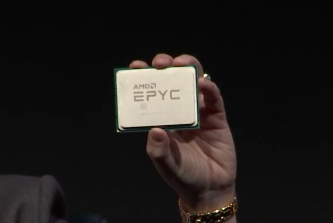
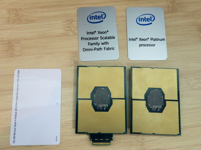
The only similarity is that both server packages are huge. Above you see the two new Xeon packages –with and without an Omni-Path connector – both of which are as big as a keycard. And below you can see how one EPYC CPU fills the hand of AMD's CEO Dr. Lisa Su.
Both are 64 bit x86 CPUs, but that is where the similarities end. For those of you who have been reading Ian's articles closely, this is no surprise. The consumer-focused Skylake-X is the little brother of the newly launched Xeon "Purley", both of which are cut from the same cloth that is the Skylake-SP family. In a nutshell, the Skylake-SP family introduces the following new features:
- AVX-512 (Many different variants of the ISA extension are available)
- A 1 MB (instead of a 256 KB) L2-cache with a non-inclusive L3
- A mesh topology to connected the cores and L3-cache chunks together
Meanwhile AMD's latest EPYC Server CPU was launched a few weeks ago:
On the package are four silicon dies, each one containing the same 8-core silicon we saw in the AMD Ryzen processors. Each silicon die has two core complexes, each of four cores, and supports two memory channels, giving a total maximum of 32 cores and 8 memory channels on an EPYC processor. The dies are connected by AMD’s newest interconnect, the Infinity Fabric...
In the next pages, we will be discussing the impact of these architectural choices on server software.
AMD's EPYC Server CPU
If you have read Ian's articles about Zen and EPYC in detail, you can skip this page. For those of you who need a refresher, let us quickly review what AMD is offering.
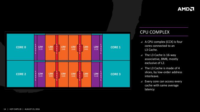
The basic building block of EPYC and Ryzen is the CPU Complex (CCX), which consists of 4 vastly improved "Zen" cores, connected to an L3-cache. In a full configuration each core technically has its own 2 MB of L3, but access to the other 6 MB is rather speedy. Within a CCX we measured 13 ns to access the first 2 MB, and 15 to 19 ns for the rest of the 8 MB L3-cache, a difference that's hardly noticeable in the grand scheme of things. The L3-cache acts as a mostly exclusive victim cache.
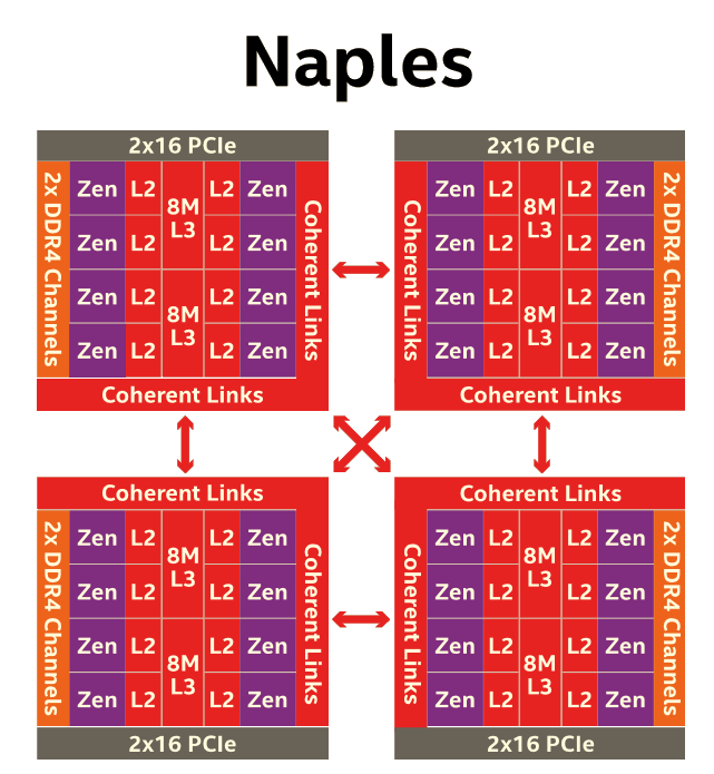
Two CCXes make up one Zeppelin die. A custom fabric – AMD's Infinity Fabric – ties together two CCXes, the two 8 MB L3-caches, 2 DDR4-channels, and the integrated PCIe lanes. That topology is not without some drawbacks though: it means that there are two separate 8 MB L3 caches instead of one single 16 MB LLC. This has all kinds of consequences. For example the prefetchers of each core make sure that data of the L3 is brought into the L1 when it is needed. Meanwhile each CCX has its own separate (not inside the L3, so no capacity hit) and dedicated SRAM snoop directory (keeping track of 7 possible states). In other words, the local L3-cache communicates very quickly with everything inside the same CCX, but every data exchange between two CCXes comes with a tangible latency penalty.
Moving further up the chain, the complete EPYC chip is a Multi Chip Module(MCM) containing 4 Zeppelin dies.
AMD made sure that each die is only one hop apart from the other, ensuring that the off-die latency is as low as reasonably possible.
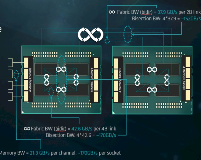
Meanwhile scaling things up to their logical conclusion, we have 2P configurations. A dual socket EPYC setup is in fact a "virtual octal socket" NUMA system.
AMD gave this "virtual octal socket" topology ample bandwidth to communicate. The two physical sockets are connected by four bidirectional interconnects, each consisting of 16 PCIe lanes. Each of these interconnect links operates at +/- 38 GB/s (or 19 GB/s in each direction).
So basically, AMD's topology is ideal for applications with many independently working threads such as small VMs, HPC applications, and so on. It is less suited for applications that require a lot of data synchronization such as transactional databases. In the latter case, the extra latency of exchanging data between dies and even CCX is going to have an impact relative to a traditional monolithic design.
AMD’s EPYC 7000-Series Processors
As announced back at the official launch, AMD is planning to hit both the dual socket and single socket markets. With up to 32 cores, 64 threads, 2TB/socket support and 128 PCIe lanes per CPU, they believe that by offering a range of core counts and frequencies, they have the nous to attack Intel, even if it comes at a slight IPC disadvantage.
AMD’s main focus will be on the 2P parts, where each CPU will use 64 PCIe lanes (using the Infinity Fabric protocol) to connect to each other, meaning that in a 2P system there will still be 128 PCIe 3.0 lanes to go around for add-in devices. There will be the top four SKUs available initially, and the other parts should be in the hands of OEMs by the end of July. All the CPUs will have access to all 64MB of the L3 cache, except the 7200-series which will have access to half.
The new processors from AMD are called the EPYC 7000 series, with names such as EPYC 7301 and EPYC 7551P. The naming of the CPUs is as follows:
EPYC 7551P
- EPYC = Brand
- 7 = 7000 Series
- 30/55 = Dual Digit Number indicative of stack positioning / performance (non-linear)
- 1 = Generation
- P = Single Socket, not present in Dual Socket
So in the future, we will see second generation ‘EPYC 7302’ processors, or if AMD scales out the design there may be EPYC 5000 processors with fewer silicon dies inside, or EPYC 3000 with a single die but for the EPYC platform socket (obviously, those last two are speculation).
But starting with the 2P processors:
| AMD EPYC Processors (2P) | |||||||||
| Cores Threads |
Frequency (GHz) | L3 | DRAM | PCIe | TDP | Price | |||
| Base | All | Max | |||||||
| EPYC 7601 | 32 / 64 | 2.20 | 2.70 | 3.2 | 64 MB | 8-Ch DDR4 2666 MT/s |
8 x16 128 PCIe |
180W | $4200 |
| EPYC 7551 | 32 / 64 | 2.00 | 2.55 | 3.0 | 180W | >$3400 | |||
| EPYC 7501 | 32 / 64 | 2.00 | 2.60 | 3.0 | 155W/170W | $3400 | |||
| EPYC 7451 | 24 / 48 | 2.30 | 2.90 | 3.2 | 180W | >$2400 | |||
| EPYC 7401 | 24 / 48 | 2.00 | 2.80 | 3.0 | 155W/170W | $1850 | |||
| EPYC 7351 | 16 / 32 | 2.40 | 2.9 | 155W/170W | >$1100 | ||||
| EPYC 7301 | 16 / 32 | 2.20 | 2.7 | 155W/170W | >$800 | ||||
| EPYC 7281 | 16 / 32 | 2.10 | 2.7 | 32 MB | 155W/170W | $650 | |||
| EPYC 7251 | 8 / 16 | 2.10 | 2.9 | 120W | $475 | ||||
The top part is the EPYC 7601, which is the CPU we were provided for in this comparison. This is a 32-core part with simultaneous multithreading, a TDP of 180W and a tray price of $4200. As the halo part, it also gets the good choice on frequencies: 2.20 GHz base, 3.2 GHz at max turbo (up to 12 cores active) and 2.70 GHz when all cores are active.
Moving down the stack, AMD will offer 24, 16 and 8-core parts. These will disable 1, 2 and 3 cores per CCX respectively, as we saw with the consumer Ryzen processors, and is done in order to keep core-to-core latencies more predictable (as well as keeping access to all the L3 cache). What is interesting to note is that AMD will offer a 32-core part at 155W (when using DDR4-2400) for $3400, which is expected to be very competitive compared to Intel (and support 2.66x more DRAM per CPU).
The 16-core EPYC 7281, while having half the L3, will be available for $650, making an interesting 2P option. Even the bottom processor at the stack, the 8-core EPYC 7251, will support the full 2TB of DRAM per socket as well as 128 PCIe lanes, making it a more memory focused SKU and having almost zero competition on these sorts of builds from Intel. For software that requires a lot of memory but pays license fees per core/socket, this is a nice part.
For single socket systems, AMD will offer the following three processors:
| AMD EPYC Processors (1P) | |||||||||
| Cores Threads |
Frequency (GHz) | L3 | DRAM | PCIe | TDP | Price | |||
| Base | All | Max | |||||||
| EPYC 7551P | 32 / 64 | 2.0 | 2.6 | 3.0 | 64 MB | 8-Ch DDR4 2666 MT/s |
8 x16 128 PCIe |
180W | $2100 |
| EPYC 7401P | 24 / 48 | 2.0 | 2.8 | 3.0 | 155W/170W | $1075 | |||
| EPYC 7351P | 16 / 32 | 2.4 | 2.9 | 155W/170W | $750 | ||||
These processors mirror the specifications of the 2P counterparts, but have a P in the name and slightly different pricing.
Introducing Skylake-SP: The Xeon Scalable Processor Family
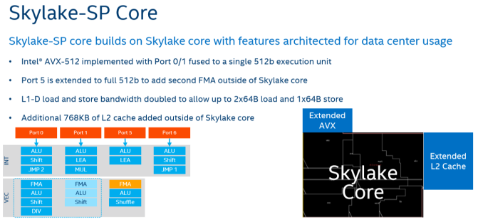
The biggest news hitting the streets today comes from the Intel camp, where the company is launching their Skylake-SP based Xeon Scalable Processor family. As you have read in Ian's Skylake-X review, the new Skylake-SP core has been rather significantly altered and improved compared to it's little brother, the original Skylake-S. Three improvements are the most striking: Intel added 768 KB of per-core L2-cache, changed the way the L3-cache works while significantly shrinking its size, and added a second full-blown 512 bit AVX-512 unit.
On the defensive and not afraid to speak their mind about the competition, Intel likes to emphasize that AMD's Zen core has only two 128-bit FMACs, while Intel's Skylake-SP has two 256-bit FMACs and one 512-bit FMAC. The latter is only useable with AVX-512. On paper at least, it would look like AMD is at a massive disadvantage, as each 256-bit AVX 2.0 instruction can process twice as much data compared to AMD's 128-bit units. Once you use AVX-512 bit, Intel can potentially offer 32 Double Precision floating operations, or 4 times AMD's peak.
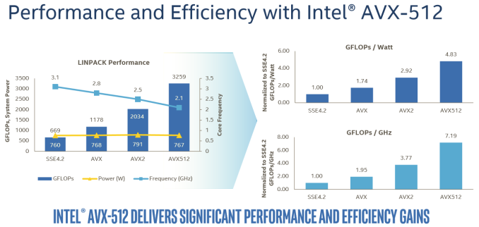
The reality, on the other hand, is that the complexity and novelty of the new AVX-512 ISA means that it will take a long time before most software will adopt it. The best results will be achieved on expensive HPC software. In that case, the vendor (like Ansys) will ask Intel engineers to do the heavy lifting: the software will get good AVX-512 support by the expensive process of manual optimization. Meanwhile, any software that heavily relies on Intel's well-optimized math kernel libraries should also see significant gains, as can be seen in the Linpack benchmark.
In this case, Intel is reporting 60% better performance with AVX-512 versus 256-bit AVX2.
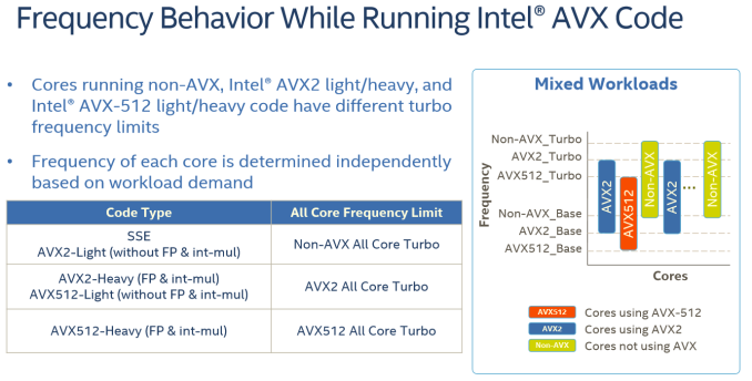
For the rest of us mere mortals, it will take a while before compilers will be capable of producing AVX-512 code that is actually faster than the current AVX binaries. And when they do, the result will be probably be limited, as compilers still have trouble vectorizing code from scratch. Meanwhile it is important to note that even in the best-case scenario, some of the performance advantage will be negated by the significantly lower clock speeds (base and turbo) that Intel's AVX-512 units run at due to the sheer power demands of pushing so many FLOPS.
For example, the Xeon 8176 in this test can boost to 2.8 GHz when all cores are active. With AVX 2.0 this is reduced to 2.4 GHz (-14%), with AVX-512, the clock tumbles down to 1.9 GHz (another 20% lower). Assuming you can fill the full width of the AVX unit, each step still sees a significant performance improvement, but AVX2 to AVX-512 won't offer a full 2x performance improvement even with ideal code.
Lastly, about half of the major floating point intensive applications can be accelerated by GPUs. And many FP applications are (somewhat) limited by memory bandwidth. While those will still benefit from better AVX code, they will show diminishing returns as you move from 256-bit AVX to 512-bit AVX. So most FP applications will not achieve the kinds of gains we saw in the well-optimized Linpack binaries.
Intel's New On-Chip Topology: A Mesh
Since the introduction of the "Nehalem" CPU architecture – and the Xeon 5500 that started almost a decade-long reign for Intel in the datacenter – Intel's engineers have relied upon a low latency, high bandwidth ring to connect their cores with their caches, memory controllers, and I/O controllers.
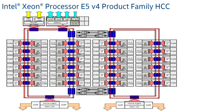
Intel's most recent adjustment to their ring topology came with the Ivy Bridge-EP (Xeon E5 2600 v2) family of CPUs. The top models were the first with three columns of cores connected by a dual ring bus, which utilized both outer and inner rings. The rings moved data in opposite directions (clockwise/counter-clockwise) in order to minimize latency by allowing data to take the shortest path to the destination. As data is brought onto the ring infrastructure, it must be scheduled so that it does not collide with previous data.
The ring topology had a lot of advantages. It ran very fast, up to 3 GHz. As result, the L3-cache latency was pretty low: if the core is lucky enough to find the data in its own cache slice, only one extra cycle is needed (on top of the normal L1-L2-L3 latency). Getting a cacheline of another slice can cost up to 12 cycles, with an average cost of 6 cycles.
However the ring model started show its limits on the high core count versions of the Xeon E5 v3, which had no less than four columns of cores and LLC slices, making scheduling very complicated: Intel had to segregate the dual ring buses and integrate buffered switches. Keeping cache coherency performant also became more and more complex: some applications gained quite a bit of performance by choosing the right snoop filter mode (or alternatively, lost a lot of performance if they didn't pick the right mode). For example, our OpenFOAM benchmark performance improved by almost 20% by choosing "Home Snoop" mode, while many easy to scale, compute-intensive applications preferred "Cluster On Die" snooping mode.
In other words, placing 22 (E7:24) cores, several PCIe controllers, and several memory controllers was close to the limit what a dual ring could support. In order to support an even larger number of cores than the Xeon v4 family, Intel would have to add a third ring, and ultimately connecting 3 rings with 6 columns of cores each would be overly complex.
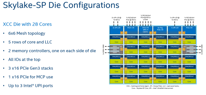
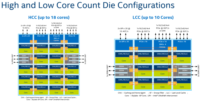
Given that, it shouldn't come as a surprise that Intel's engineers decided to use a different topology for Skylake-SP to connect up to 28 cores with the "uncore." Intel's new solution? A mesh architecture.
Under Intel's new topology, each node – a caching/home agent, a core, and a chunk of LLC – is interconnected via a mesh. Conceptually it is very similar to the mesh found on Xeon Phi, but not quite the same. In the long-run the mesh is far more scalable than Intel's previous ring topology, allowing Intel to connect many more nodes in the future.
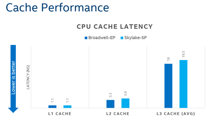
How does it compare to the ring architecture? The Ring could run at up to 3 GHz, while the current mesh and L3-cache runs at at between 1.8GHZ and 2.4GHz. On top of that, the mesh inside the top Skylake-SP SKUs has to support more cores, which further increases the latency. Still, according to Intel the average latency to the L3-cache is only 10% higher, and the power usage is lower.
A core that access an L3-cache slice that is very close (like the ones vertically above each other) gets an additional latency of 1 cycle per hop. An access to a cache slice that is vertically 2 hops away needs 2 cycles, and one that is 2 hops away horizontally needs 3 cycles. A core from the bottom that needs to access a cache slice at the top needs only 4 cycles. Horizontally, you get a latency of 9 cycles at the most. So despite the fact that this Mesh connects 6 extra cores verse Broadwell-EP, it delivers an average latency in the same ballpark (even slightly better) as the former's dual ring architecture with 22 cores (6 cycles average).
Meanwhile the worst case scenario – getting data from the right top node to the bottom left node – should demand around 13 cycles. And before you get too concerned with that number, keep in mind that it compares very favorably with any off die communication that has to happen between different dies in (AMD's) Multi Chip Module (MCM), with the Skylake-SP's latency being around one-tenth of EPYC's. It is crystal clear that there will be some situations where Intel's server chip scales better than AMD's solution.
There are other advantages that help Intel's mesh scale: for example, caching and home agents are now distributed, with each core getting one. This reduces snoop traffic and reduces snoop latency. Also, the number of snoop modes is reduced: no longer do you need to choose between home snoop or early snoop. A "cluster-on-die" mode is still supported: it is now called sub-NUMA Cluster or SNC. With SNC you can divide the huge Intel server chips into two NUMA domains to lower the latency of the LLC (but potentially reduce the hitrate) and limit the snoop broadcasts to one SNC domain.
Intel's Optimized Turbo Profiles
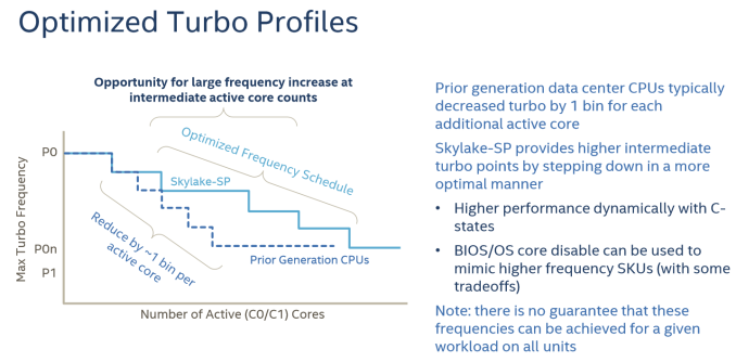
Also new to Skylake-SP, Intel has also further enhanced turbo boosting.
There are also some security and virtualization enhancements (MBE, PPK, MPX) , but these are beyond the scope this article as we don't test them.
Summing It All Up: How Skylake-SP and Zen Compare
The table below shows you the differences in a nutshell.
| AMD EPYC 7000 |
Intel Skylake-SP | Intel Broadwell-EP |
|
| Package & Dies | Four dies in one MCM | Monolithic | Monolithic |
| Die size | 4x 195 mm² | 677 mm² | 456 mm² |
| On-Chip Topology | Infinity Fabric (1-Hop Max) |
Mesh | Dual Ring |
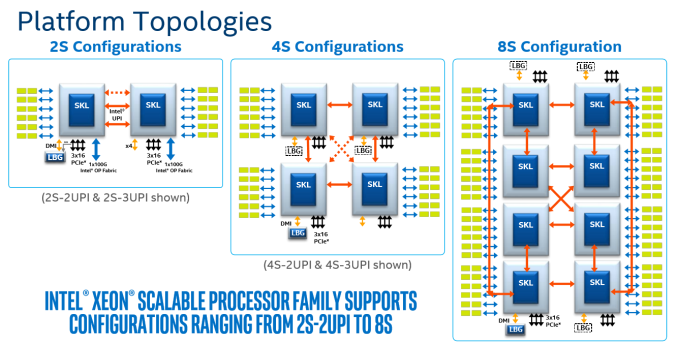
| Socket configuration | 1-2S | 1-8S ("Platinum") | 1-2S |
| Interconnect (Max.) Bandwidth (*)(Max.) |
4x16 (64) PCIe lanes 4x 37.9 GB/s |
3x UPI 20 lanes 3x 41.6 GB/s |
2x QPI 20 lanes 2x 38.4 GB/s |
| TDP | 120-180W | 70-205W | 55-145W |
| 8-32 | 4-28 | 4-22 | |
| LLC (max.) | 64MB (8x8 MB) | 38.5 MB | 55 MB |
| Max. Memory | 2 TB | 1.5 TB | 1.5 TB |
| Memory subsystem Fastest sup. DRAM |
8 channels DDR4-2666 |
6 channels DDR4-2666 |
4 channels DDR4-2400 |
| PCIe Per CPU in a 2P |
64 PCIe (available) | 48 PCIe 3.0 | 40 PCIe 3.0 |
(*) total bandwidth (bidirectional)
At a high level, I would argue that Intel has the most advanced multi-core topology, as they're capable of integrating up to 28 cores in a mesh. The mesh topology will allow Intel to add more cores in future generations while scaling consistently in most applications. The last level cache has a decent latency and can accommodate applications with a massive memory footprint. The latency difference between accessing a local L3-cache chunk and one further away is negligible on average, allowing the L3-cache to be a central storage for fast data synchronization between the L2-caches. However, the highest performing Xeons are huge, and thus expensive to manufacture.
AMD's MCM approach is much cheaper to manufacture. Peak memory bandwidth and capacity is quite a bit higher with 4 dies and 2 memory channels per die. However, there is no central last level cache that can perform low latency data coordination between the L2-caches of the different cores (except inside one CCX). The eight 8 MB L3-caches acts like - relatively low latency - spill over caches for the 32 L2-caches on one chip.
Intel’s Skylake-SP Processors: Platinum, Gold, Silver, Bronze
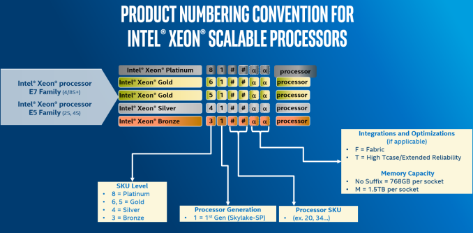
In a break from the traditional naming scheme that Intel has used for several generations, we saw the move to Platinum, Gold, Silver and Bronze SKUs for Skylake-SP. We’re told there is no real conversion between the two, and to some extent Intel is correct: it’s almost impossible to correlate what the conversion from the old chip naming is to the new chip naming is, but also Intel has decided to awkwardly complicate what the numbers in the middle mean, with no real direct pattern to follow on some of the digits. This is the diagram provided:
Aside from the name (Platinum, Gold, Silver, Bronze), the four digits indicate SKU level, Generation, and then a pair of digits for general performance level. After this there are a series of potential suffixes:
- M = Supports 1.5 TB DRAM per socket, up from 768GB as standard
- T = High T-Case, Extended Life
- F = Integrated OmniPath Fabric
This leads to the following lists for the processors. We have sorted these into numerical order, which may be different to Intel’s pricing or specification lists. First up is the Platinum parts, geared for up to 8-Socket use.
Xeon Platinum
So what is the "Platinum" all about? We were told at the briefing:
"One of the reasons for this is that sometimes a customer could take advantage of an 8-socket variant processor (due to high cache per core, for example), but would never consider it because the customer only needed a two-socket configuration. One of the reasons given for the naming is to alleviate this issue."
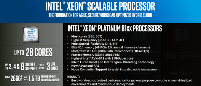
There is no longer an E7, but if you look at the prices ($3000-$13000) and features, the Xeon Platinum is clearly the successor to the E7. There is support for up to 8 sockets, and most of the Platinum SKUs have 24 to 28 cores, and is clearly using the XCC silicon.
| Intel Xeon Skylake-SP Platinum Series | ||||||||||
| Segment | Cores | Base (GHz) |
Turbo (GHz) |
L3 (MB) |
L3/core (MB) |
TDP (W) |
Price (USD) |
|||
| 8180 | Per-Core | 28 | 2.5 | 3.8 | 38.50 | 1.375 | 205 | $10009 | ||
| 8180 | M | 2xDRAM | 28 | 2.5 | 3.8 | 38.50 | 1.375 | 205 | $13011 | |
| 8176 | Perf/Watt | 28 | 2.1 | 3.8 | 38.50 | 1.375 | 165 | $8719 | ||
| 8176 | M | 2xDRAM | 28 | 2.1 | 3.8 | 38.50 | 1.375 | 165 | $11722 | |
| 8176 | F | OmniPath | 28 | 2.1 | 3.8 | 38.50 | 1.375 | 173 | $8874 | |
| 8170 | Perf/Watt | 26 | 2.1 | 3.7 | 35.75 | 1.375 | 165 | $7405 | ||
| 8170 | M | 2xDRAM | 26 | 2.1 | 3.7 | 35.75 | 1.375 | 165 | $10409 | |
| 8168 | Per-Core | 24 | 2.7 | 3.7 | 33.00 | 1.375 | 205 | $5890 | ||
| 8164 | Perf/Watt | 26 | 2.0 | 3.7 | 35.75 | 1.375 | 150 | $6114 | ||
| 8160 | Perf/Watt | 24 | 2.1 | 3.7 | 33.00 | 1.375 | 150 | $4702 | ||
| 8160 | M | 2xDRAM | 24 | 2.1 | 3.7 | 33.00 | 1.375 | 150 | $7704 | |
| 8160 | T | 10yr Life | 24 | 2.1 | 3.7 | 33.00 | 1.375 | 150 | $4936 | |
| 8160 | F | OmniPath | 24 | 2.1 | 3.7 | 33.00 | 1.375 | 160 | $4856 | |
| 8158 | Per-Core | 12 | 3.0 | 3.7 | 24.75 | 2.063 | 150 | $7007 | ||
| 8156 | Per-Core | 4 | 3.6 | 3.7 | 16.50 | 4.125 | 105 | $7007 | ||
| 8153 | Perf/Watt | 16 | 2.0 | 2.8 | 22.00 | 1.375 | 125 | $3115 | ||
I suppose the first thing to note is the pricing. If you want the extended DRAM version of the 28-core CPU, be prepared to shell out $13k for the tray pricing. That is almost 2x the cost of the highest-end previous generation part, and becomes a sizeable chunk of any build. The standard DRAM support version is ‘only’ $10k. For anyone around the $7-8k per CPU budget, like last generation, you can still get a 28-core processor in the form of the 8176, or 8170 if you can give up a couple of cores.
With the double DRAM supported parts, the 30% premium seems rather high. We were told from Intel that ‘only 0.5% of the market actually uses those quad ranked and LR DRAMs’, although that more answers the fact that the base support is 768GB, not that the 1.5GB parts have an extra premium.
This pricing seems crazy, but it is worth pointing out a couple of things. The companies that buy these parts, namely the big HPC clients, do not pay these prices. They’ll likely pay under half these prices, and probably much less. Nonetheless, this is still a sizeable jump over the last generation – exact pricing for the top tier customers will be in their contracts, but it has been predicted by some analysts that there might be a small outcry, even from Intel’s largest customers.
A few users might be confused about the Platinum 8156, a quad core part at $7007. This is a high cache/core part, offering 4.125 MB of L3 per core, up from 1.375MB per core for the standard parts. Intel has offered these parts for a few generations now, for customers that find their code to be L3 sensitive or have licensing agreements base on per-core/per-socket as well. What customers will have to note is that Skylake-SP has a different L3 cache compared to previous generations, by being a non-inclusive cache (and essentially a victim cache) means it will be used very differently. With a larger L2 cache as well, the L3 might become less important, or the fact it becomes a victim cache might make it useful/useless on the code. For customers after these sorts of cores, it is worth profiling the code on the CPU first, just to make sure.
Xeon Gold
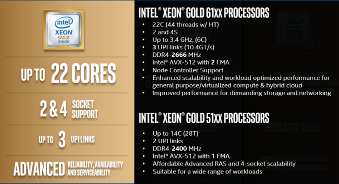
Despite some of the nuance, the Platinum processor list is easy to follow, especially by comparison to the Gold list. The Gold processors are technically split into two groups, the Gold 6100 series, and Gold 5100 series: split in their DRAM and AVX-512 support, as well as the number of UPI links.
The Gold 6100-series will have 2 FMA units per core rather than one, showing that the Port-5 FMA is enabled and can feed the AVX-512 unit better for up to 2x performance. (This is similar to what we saw with the consumer Skylake-X parts, where >10-core parts have both FMAs enabled.) The 6100-series also has DDR4-2666 support, whereas the 5100-series is limited to DDR4-2400 as standard.
There’s also a matter of UPI links to other processors. This matters when these processors are in a quad-socket system: with only 2 UPI links for the 5100-series, that means the processors are in a ring arrangement, rather than a hatch-arrangement, and to access data on the opposite side of the ring requires two hops, rather than the one hop on the hatch. This is perhaps a niche issue, but one worth taking note of.
| Intel Xeon Skylake-SP Gold Series | ||||||||||
| Segment | Cores | Base (GHz) |
Turbo (GHz) |
L3 (MB) |
L3/core (MB) |
TDP (W) |
Price (USD) |
|||
| 6154 | Per-Core | 18 | 3.0 | 3.7 | 24.75 | 1.375 | 200 | $3543 | ||
| 6152 | Perf/Watt | 22 | 2.1 | 3.7 | 30.25 | 1.375 | 140 | $3655 | ||
| 6150 | Per-Core | 18 | 2.7 | 3.7 | 24.75 | 1.375 | 165 | $3358 | ||
| 6148 | Per-Core | 20 | 2.4 | 3.7 | 27.50 | 1.375 | 150 | $3072 | ||
| 6148 | F | OmniPath | 20 | 2.4 | 3.7 | 27.50 | 1.375 | 160 | $3227 | |
| 6146 | Per-Core | 12 | 3.2 | 4.2 | 24.75 | 2.063 | 165 | $3286 | ||
| 6144 | Per-Core | 8 | 3.5 | 4.2 | 24.75 | 3.094 | 150 | $2925 | ||
| 6142 | Per-Core | 16 | 2.6 | 3.7 | 22.00 | 1.375 | 150 | $2946 | ||
| 6142 | M | 2x DRAM | 16 | 2.6 | 3.7 | 22.00 | 1.375 | 150 | $5949 | |
| 6142 | F | OmniPath | 16 | 2.6 | 3.7 | 22.00 | 1.375 | 160 | $3101 | |
| 6140 | Perf/Watt | 18 | 2.3 | 3.7 | 24.75 | 1.375 | 140 | $2445 | ||
| 6140 | M | 2x DRAM | 18 | 2.3 | 3.7 | 24.75 | 1.375 | 140 | $5448 | |
| 6138 | Perf/Watt | 20 | 2.0 | 3.7 | 27.50 | 1.375 | 125 | $2612 | ||
| 6138 | T | 10yr Life | 20 | 2.0 | 3.7 | 27.50 | 1.375 | 125 | $2742 | |
| 6138 | F | OmniPath | 20 | 2.0 | 3.7 | 27.50 | 1.375 | 135 | $2767 | |
| 6136 | Per-Core | 12 | 3.0 | 3.7 | 24.75 | 2.063 | 150 | $2460 | ||
| 6134 | Per-Core | 8 | 3.2 | 3.7 | 24.75 | 3.094 | 130 | $2214 | ||
| 6134 | M | 2x DRAM | 8 | 3.2 | 3.7 | 24.75 | 3.094 | 130 | $5217 | |
| 6132 | Per-Core | 14 | 2.6 | 3.7 | 19.25 | 1.375 | 140 | $2111 | ||
| 6130 | Perf/Watt | 16 | 2.1 | 3.7 | 22.00 | 1.375 | 125 | $1894 | ||
| 6130 | T | 10yr Life | 16 | 2.1 | 3.7 | 22.00 | 1.375 | 125 | $1988 | |
| 6130 | F | OmniPath | 16 | 2.1 | 3.7 | 22.00 | 1.375 | 135 | $2049 | |
| 6128 | Per-Core | 6 | 3.4 | 3.7 | 19.25 | 3.208 | 115 | $1691 | ||
| 6126 | Per-Core | 12 | 2.6 | 3.7 | 19.25 | 1.604 | 125 | $1776 | ||
| 6126 | T | 10yr Life | 12 | 2.6 | 3.7 | 19.25 | 1.604 | 125 | $1865 | |
| 6126 | F | OmniPath | 12 | 2.6 | 3.7 | 19.25 | 1.604 | 135 | $1931 | |
| 5122 | Per-Core | 4 | 3.6 | 3.7 | 16.50 | 4.125 | 105 | $1221 | ||
| 5120 | Perf/Watt | 14 | 2.2 | 3.2 | 19.25 | 1.375 | 105 | $1555 | ||
| 5120 | T | 10yr Life | 14 | 2.2 | 3.2 | 19.25 | 1.375 | 105 | $1727 | |
| 5119 | T | 10yr Life | 14 | 1.9 | - | 19.25 | 1.375 | 85 | $1555 | |
| 5118 | Perf/Watt | 12 | 2.3 | 3.2 | 16.50 | 1.375 | 105 | $1273 | ||
| 5115 | Perf/Watt | 10 | 2.4 | 3.2 | 13.75 | 1.375 | 85 | $1221 | ||
Why all those differences between the two grades of Gold did not result in a separate "grade" for the 51xx is beyond me. For example, for the HPC people, the 51xx gets you slower DRAM and half the FP peak performance. The only logical way to describe the Gold grade is "the 4 socket version with wildly varying features".
Xeon Silver and Xeon Bronze
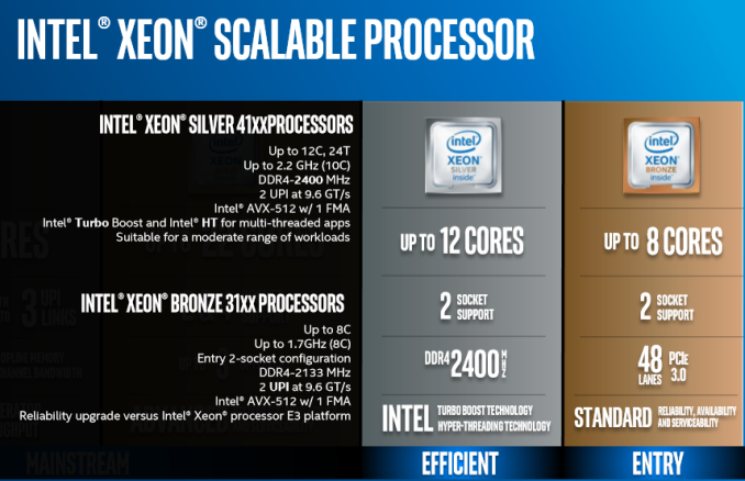
After 16 CPUs for Platinum and 32 CPUs in Gold, the Silver and Bronze parts only have 10 in total. These parts support two sockets at most, and only up to 12 cores, showing that Intel’s market segmentation strategy has changed significantly here. In the last generation, a customer could get a dual-socket high-core-count part like the E5-2699A v4 without the need to look at 8-socket parts, but now Intel has that limited such that you have to look at Gold or Platinum processors to play in this space.
As with the Gold 5100 series, these Silver and Bronze parts only have 1 FMA per core for the AVX-512. The Silver parts support DDR4-2400, hyperthreading, and UPI at 9.6 GT/s (down from 10.4 GT/s on Gold), compared to the Bronze CPUs that use DDR4-2133, no hyperthreading, the slower UPI, but also slower in general – peak frequencies are at 1.7 GHz with AVX-512 at 0.8 GHz.
| Intel Xeon Skylake-SP Silver and Bronze Series | ||||||||||
| Segment | Cores | Base (GHz) |
Turbo (GHz) |
L3 (MB) |
L3/core (MB) |
TDP (W) |
Price (USD) |
|||
| 4116 | Perf/Watt | 12 | 2.1 | 3.0 | 16.50 | 1.375 | 85 | $1002 | ||
| 4116 | T | 10yr Life | 12 | 2.1 | 3.0 | 16.50 | 1.375 | 85 | $1112 | |
| 4114 | Perf/Watt | 10 | 2.2 | 3.0 | 13.75 | 1.375 | 85 | $694 | ||
| 4114 | T | 10yr Life | 10 | 2.2 | 3.0 | 13.75 | 1.375 | 85 | $773 | |
| 4112 | Perf/Watt | 4 | 2.6 | 3.0 | 5.50 | 1.375 | 85 | $473 | ||
| 4110 | Perf/Watt | 8 | 2.1 | 3.0 | 11.00 | 1.375 | 85 | $501 | ||
| 4109 | T | 10yr Life | 8 | 2.0 | 3.0 | 11.00 | 1.375 | 70 | $501 | |
| 4108 | Perf/Watt | 8 | 1.8 | 3.0 | 11.00 | 1.375 | 85 | $417 | ||
| 3106 | Perf/Watt | 8 | 1.7 | - | 11.00 | 1.375 | 85 | $306 | ||
| 3104 | Perf/Watt | 6 | 1.7 | - | 8.25 | 1.375 | 85 | $213 | ||
Overview
It is worth noting that Intel’s documents, such as the price lists do not list these parts in numerical order. At times the higher core count part will be listed higher than a lower core count part with more cache/frequency, and this will be non-obvious, especially when quick glancing. In general, the higher the number, the higher the raw performance is (Cores, frequency), but this does not always hold true.
The Platinum 8170 (165W) has only 2 cores (8%, 26 vs 24) more than the 8168 (205W), but the latter has an almost 30% higher frequency (2.7 vs 2.1). So maybe the higher the number, the better the performance/watt? This doesn’t hold either, because the 8164 (150W) runs 26 cores at a 2 GHz. The Gold 6144 and 6142 look very similar, but the former is an 8-core at 3.5 GHz (with 25 MB of L3), while the latter is a 16-core at 2.6 GHz (with 22 MB L3).
The new numbering and grade scheme has some merits, but there are still too many exceptions to rely on it. Especially the Gold grade having two sets of parts, and the last two numbers are not logical at all. You will still need to decipher every SKU at ark.intel.com to know what you are buying.
Intel’s Turbo Modes
A last minute detail from Intel yesterday was information on the Turbo modes. As expected, not all of the processors actually run at their rated/base frequency: most will apply a series of turbo modes depending on how many cores are registered as ‘active’. Each core can have its frequency adjusted independently, allowing VMs to take advantage of different workload types and not be hamstrung by occupants on other VMs in the same socket. This becomes important when AVX, AVX2 and AVX-512 are being used at the same time.
Most of the turbo modes are a sliding scale, with the peak turbo used when only one or two cores are active, sliding down to a minimum frequency that may be the ‘base’ frequency or just above it. There’s a lot of information for the parts here, so we’ll break it down into stages.
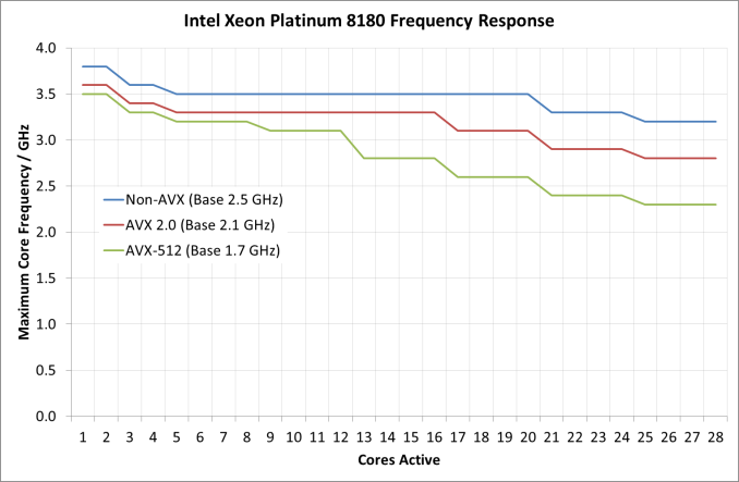
First up, a look at the Platinum 8180 in the different modes:
It should be worth noting what the base frequency actually is, and some of the nuance in Intel’s wording here. The base frequency is the guaranteed frequency of the chip – Intel sells the chip with the base frequencies as the guarantee, such that when the chip is not idle and not in normal conditions (i.e. when not in thermal power states to reduce temperature) should operate at this frequency or above it. Intel also lists the per-core turbo frequencies as ‘Maximum Core Frequencies’ indicating that the processors could be running lower than listed, depending on power distribution and requirements in other areas of the chip (such as the uncore, or memory controller). It’s a vague set of terms but ultimately the frequency is determined on the fly and can be affected by many factors, but Intel guarantees a certain amount and provides guides as to what it expects the turbo frequencies to be.
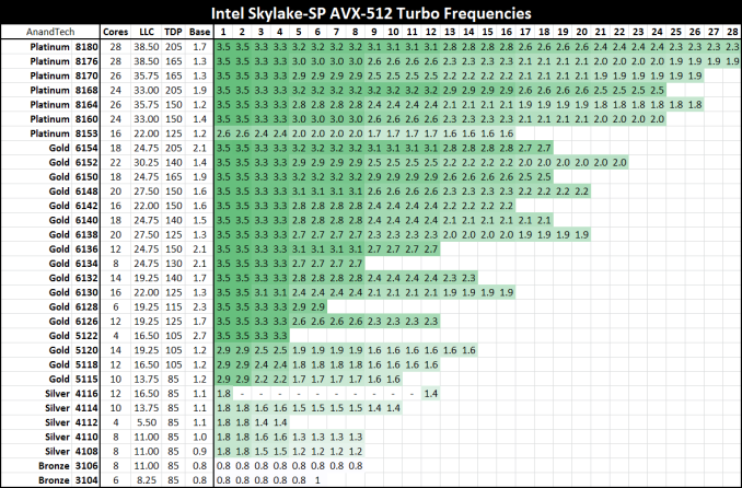
As for the Platinum 8180, it keeps its top turbo modes while up to two cores are active, and then drops down. It does this again for another two cores, and a further two cores. From this point, under non-AVX load the CPU is pretty much the same frequency until >20 cores are loaded, but does not decrease that much in all. For AVX 2.0 and AVX-512, the downward slope of more cores means less frequency continues, with AVX-512 taking a bigger jump down at 13 cores loaded. The final turbo frequency for AVX-512 running on all cores is 2.3 GHz.
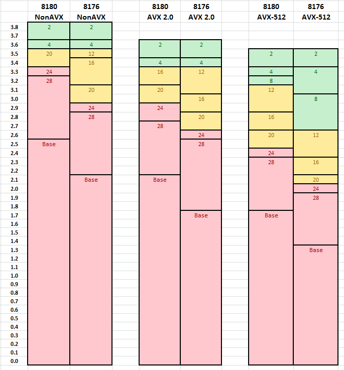
Comparing the two 28-core CPUs for which we have turbo information gives this graph. The numbers relate to the number of cores need to be loaded for that frequency.
Both processors are equal to each other for dual core loading, but the separation occurs when more cores are loaded. As we move through to AVX 2.0 and AVX-512, it is clear where the separations are in performance – to get the best for variable core loading, the more expensive processors are required.
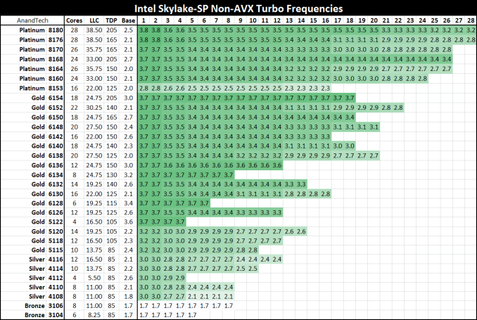
Here’s the big table for all the processors on Non-AVX loading:
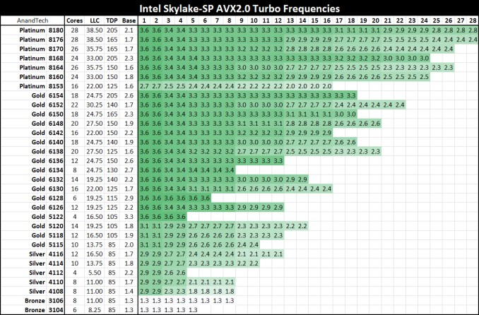
Despite the 2.0/2.1 GHz base on most of the Platinum series, all the CPUs will turbo up to 3.7-3.8 GHz on low core loading except for the lower power Platinum 8153. For users wanting to strike a good balance between the core count and frequency, the Gold 6154 is probably the place to be: 18 cores that will only ever run at 3.7 GHz with non-AVX loading (3.5-2.7 GHz on AVX-512 depending on core count), and will be $3543 as a list price at 205W. It is perhaps worth noting that this will likely top any of the Core i9 processors planned: at 18-cores and 205W for 3.7 GHz, the Core i9-7980XE which will have 18 cores but run 165W will likely be clocked lower (but also only ~$2000).
Moving onto AVX2.0 and AVX-512:
Intel Expanding the Chipset: 10 Gigabit Ethernet and QuickAssist Technology
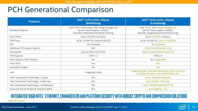
The refresh strategy from Intel on the chipset side has an ultra-long cadence. In recent memory, Intel’s platform launches are designed to support two generations of processor release, and in that time there is typically no chipset update, leaving the platform controller hub semi-static for functionality for usually three years. This is compared to the consumer side, where new chipsets are launched with every new CPU generation, with bigger jumps coming every couple of years. For the new launch today, Intel pushing the enterprise chipset ahead in a new direction.
The point of the chipset previously was to provide some basic IO support in the form of SATA/SAS ports, some USB ports, and a few PCIe lanes for simple controllers like USB 3.0, Gigabit Ethernet, or perhaps an x4 PCIe slot for a non-accelerator type card. The new chipsets, part of the C620 family codenamed Lewisburg, are designed to assist with networking, cryptography, and act more like a PCIe switch with up to 20 PCIe 3.0 lane support.
The headline features that matter most is the upgrade in DMI connection to the chipset, upgraded from DMI 2.0 to DMI 3.0 to match the consumer platforms, having those 20 PCIe 3.0 lanes from the chipset, and also the new feature under CPU Uplink.
For the new generation of Lewisburg chipsets, if an OEM requires that a platform has access to a cryptography engine or 10 Gigabit Ethernet, then they can attach 8 or 16 lanes from the processor into the chipset via this CPU Uplink port. Depending on which model of chipset is being used, this can provide up to four 10 GbE ports with iWARP RDMA, or up to 100 GB/s IPSec/SSL of QuickAssist support.
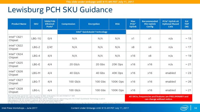
Intel will offer seven different versions of the chipset, varying in 10G and QAT support, but also varying in TDP:
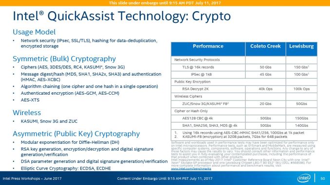
On the cryptography side, Intel has previously sold add-in PCIe cards for QuickAssist, but is now moving it onto the systems directly. By adding it into the chipset, it can be paired with the Ethernet traffic and done in-situ, and specifically Intel points to bulk cryptography (150 Gb/s AES256/SHA256), Public Key Encryption (100k ops of RSA2048) and compression (100+ Gb/s deflate).
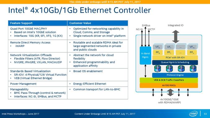
With the GbE, Intel has designed this to be paired with the X722 PHY, and supports network virtualization, traffic shaping, and supports Intel’s Data Plane Development Kit for advanced packet forwarding.
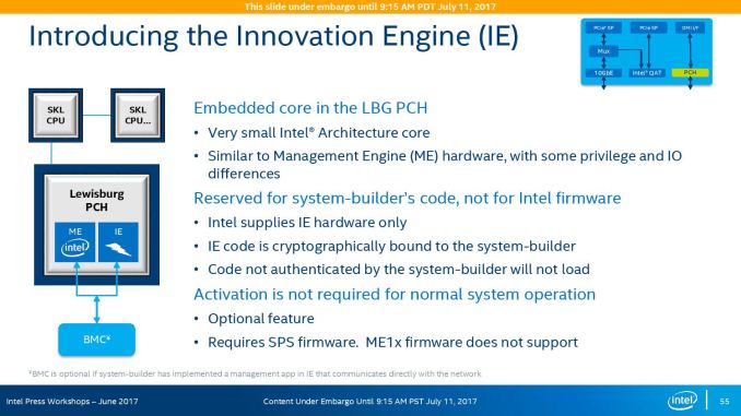
The chipset will also include a new feature called Intel’s Innovation Engine, giving a small embedded core into the PCH which mirrors Intel’s Management Engine but is designed for system-builders and integrators. This allows specialist firmware to manage some of the capabilities of the system on top of Intel’s ME, and is essentially an Intel Quark x86 core with 1.4MB SRAM.
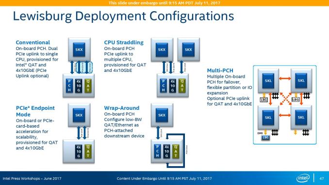
The chipsets are also designed to be supported between different CPUs within the same multi-processor system, or for a system to support multiple chipsets at once as needed.
Pricing Comparison: AMD versus Intel
We are all hoping that the renewed competition between Intel and AMD results in more bang for the buck. Intel just launched about 50 SKUs, so we made a list of those that will go head-to-head with AMD's already announced EPYC SKUs. On average, the Intel SKUs will priced slightly higher, reflecting the fact that Intel believes buyers are willing to pay a bit more for the vendor with the better track record.
| AMD EPYC Processors (2P) | Intel Xeon Processoors (2-8P) | ||||||
| AMD EPYC SKU |
Cores |
Freq (GHz) Base-Max |
Price | Intel Xeon SKU |
Cores | Freq (GHz) Base-Max |
Price |
| Xeon 8180 (205W) | 28 | 2.5-3.8 | $10009 | ||||
| Xeon 8176M (165W) | 28 | 2.1-3.8 | $11722 | ||||
| Xeon 8176 (165W) | 28 | 2.1-3.8 | $8719 | ||||
| EPYC 7601 (180W) |
32 | 2.2 -3.2 | $4200 | Xeon 8160 (150W) | 24 | 2.1-3.7 | $4702 |
| EPYC 7551 (180W) |
32 | 2.0-3.0 | >$3400 | Xeon 6152 (140W) | 22 | 2.1-3.7 | $3655 |
| EPYC 7501 (155/170W) | 32 | 2.0-3.0 | $3400 | Xeon 6150 (165W) | 18 | 2.7-3.4 | $3358 |
| EPYC 7451 (180W) |
24 | 2.3-3.2 | >$2400 | Xeon 6140 (165W) | 18 | 2.3-3.7 | $2445 |
| EPYC 7401 (155/170W) | 24 | 2.0-3.0 | $1850 | Xeon 6130 (125W) | 16 | 2.1-3.7 | $1894 |
| Xeon 5120 (105W) | 14 | 2.2-3.2 | $1555 | ||||
| EPYC 7351 (155/170W) | 16 | 2.4-2.9 | >$1100 | Xeon 5118 (105W) | 12 | 2.3-3.2 | $1221 |
| EPYC 7301 (155/170W) | 16 | 2.2-2.7 | >$800 | Xeon 4116 (85W) |
12 | 2.1-3.0 | $1002 |
| EPYC 7281 (155/170W) | 16 | 2.1-2.7 | $650 | Xeon 4114 (85W) |
10 | 2.2-3.0 | $694 |
| EPYC 7251 (120W) |
8 | 2.1-2.9 | $475 | Xeon 4110 (85W) |
8 | 2.1-3.0 | $501 |
Several trends pop up as we look at the table above.
First of foremost, those 24-28 core CPUs are a wonder of modern multicore CPU architecture, but you sure have to pay a lot of money for them. This is especially the case for the SKUs that can support 1.5 TB per socket. Of course if you can afford SAP Hana, you can afford $10k CPUs (or so the theory goes).
Still, if we compare the new high-end Skylake-EP SKUs with the previous 22-core Xeon E5-2699 v4 ($4199), paying twice as much for a 28-core chip just because it can be used in 8 socket configuration is bad news for those of us who need a very fast 2 socket system. In fact, it is almost as Intel has no competition: we only get a little more performance for the same price. For example you can get a Xeon 6148 (20 cores at 2.4 GHz, 150W TDP) for $3072, while you had to pay $3228 last generation for a Xeon E5-2698 v4 (20 cores at 2.2 GHz, 135W). The latter had smaller L2-caches but a much larger L3-cache (45 MB vs 27.5 MB). We're still not getting big steps forward on a performance-per-dollar basis, a similar problem we had with the launch of the Xeon E5 v4 last year.
Hopefully, AMD's EPYC can put some pressure on Intel, if not exceed the 800lb gorilla entirely. AMD typically offers many more cores for the same price. At the high end, AMD offers up to 10 more cores than the similar Xeon: compare the EPYC 7551 with the Intel Xeon 6152.
On the other hand, Intel offers lower TDPs and higher turbo clocks. The 16-core EPYC CPUs in particular seem to have remarkably high TDPs compared to similar Intel SKUs. Those 16-cores look even worse as, despite the lower core count and high TDP, the turbo clock is lower than 3 GHz.
In a nutshell: looking at the current lineups we want lower prices from Intel, and more attractive mid-range SKUs from AMD.
| AMD EPYC Processors (1P) | ||||
| Cores Threads |
Frequency (GHz) | TDP | Price | |
| EPYC 7551P | 32 / 64 | 2.0 -3.0 | 180W | $2100 |
| EPYC 7401P | 24 / 48 | 2.0-3.0 | 155W/170W | $1075 |
| EPYC 7351P | 16 / 32 | 2.4-2.9 | 155W/170W | $750 |
Finally, AMD's single-socket SKUs – identified by a P suffix – are by far the most interesting to us and the most dangerous to Intel. It will be interesting to see how well two 12-core Xeon 5118s can compete with one EPYC 7551P. The clocks are similar, but AMD has 8 extra cores, a less complex server board, much more PCIe bandwidth, and a lower TDP. AMD should have serious cost advantage on paper. We hope to check that in a later review.
Testing Notes
For the EPYC launch, AMD sent us their best SKU: the EPYC 7601. Meanwhile Intel gave us a choice between the top bin Xeon 8180 and the Xeon 8176. Considering that the latter had 165-173W TDP, similar to AMD's best EPYC, we felt that the Xeon 8176 was the best choice.
Unfortunately, our time testing the two platforms has been limited. In particular, we only received AMD's EPYC system last week, and the company did not put an embargo on the results. This means that we can release the data now, in time to compare it to the new Skylake-SP Xeons, however it also means that we've only had a handful of days to work with the platform before writing all of this up for today's embargo. We're confident in the data, but it means that we haven't had a chance to tease out the nuances of EPYC quite yet, and that will have to be something we get to in a future article.
Meanwhile we should note that we've had to retire the bulk of our historical benchmark data, as we upgraded both our compiler and OS (see below). Due to this, we only had a very limited amount of time to run additional systems, and for that reason we've opted include Intel's Xeon E5-2690. The Sandy Bridge-EP processor is about 5 years old, and for customers who aren't upgrading their servers every single generation, it's these servers that we believe are most likely to get upgraded in this round. So for server managers looking at finally buying into new hardware, you can get an idea of much return of investment you get.
Benchmark Configuration and Methodology
All of our testing was conducted on Ubuntu Server "Xenial" 16.04.2 LTS (Linux kernel 4.4.0 64 bit). The compiler that ships with this distribution is GCC 5.4.0.
You will notice that the DRAM capacity varies among our server configurations. The reason is that we had little time left before today's launch embargo. Removing any hardware is always a risk, so we decided to run our tests without significantly changing the internal hardware of the systems we received from AMD and Intel (SSDs were still replaced). As far as we know, all of our tests fit in 128 GB, so DRAM capacity should not have much influence on performance. But it wil have a impact on total energy consumption, which we will discuss.
Last but not least, we want to note how the performance graphs have been color-coded. Orange is AMD's EPYC, dark blue is Intel's best (Skylake-SP), and light blue is the previous generation Xeons (Xeon E5-v4) . Gray has been used for the soon-to-be-replaced Xeon v1.
Intel's Xeon "Purley" Server – S2P2SY3Q (2U Chassis)
| CPU | Two Intel Xeon Platinum 8176 (2.1 GHz, 28c, 38.5MB L3, 165W) |
| RAM | 384 GB (12x32 GB) Hynix DDR4-2666 |
| Internal Disks | SAMSUNG MZ7LM240 (bootdisk) Intel SSD3710 800 GB (data) |
| Motherboard | Intel S2600WF (Wolf Pass baseboard) |
| Chipset | Intel Wellsburg B0 |
| BIOS version | 9/02/2017 |
| PSU | 1100W PSU (80+ Platinum) |
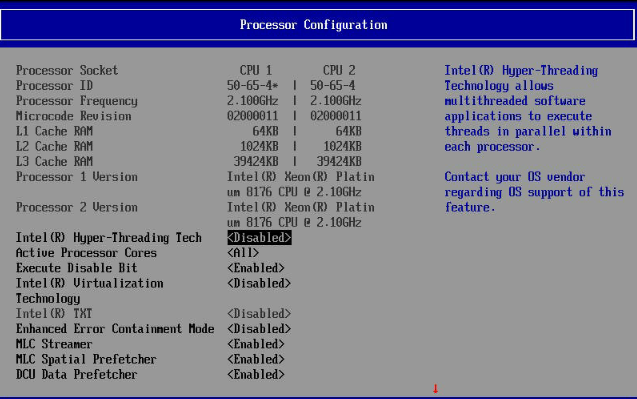
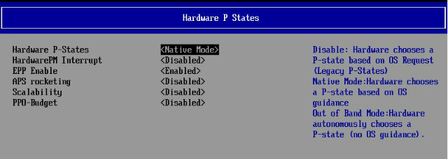
The typical BIOS settings can be seen below; we enabled hyperthreading and Intel virtualization.
AMD EPYC 7601 – (2U Chassis)
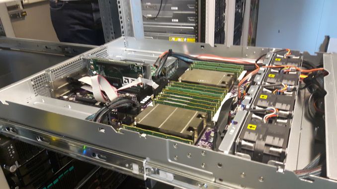
Five years after our "Piledriver review", a new AMD server arrives in the Sizing Servers Lab.
| CPU | Two EPYC 7601 (2.2 GHz, 32c, 8x8MB L3, 180W) |
| RAM | 512 GB (16x32 GB) Samsung DDR4-2666 @2400 |
| Internal Disks | SAMSUNG MZ7LM240 (bootdisk) Intel SSD3710 800 GB (data) |
| Motherboard | AMD Speedway |
| BIOS version | To check. |
| PSU | 1100W PSU (80+ Platinum) |
Intel's Xeon E5 Server – S2600WT (2U Chassis)
| CPU | Two Intel Xeon processor E5-2699v4 (2.2 GHz, 22c, 55MB L3, 145W) Two Intel Xeon processor E5-2690v3 (2.3 GHz, 14c, 35MB L3, 120W) |
| RAM | 256 GB (16x16GB) Kingston DDR-2400 |
| Internal Disks | SAMSUNG MZ7LM240 (bootdisk) Intel SSD3700 800 GB (data) |
| Motherboard | Intel Server Board Wildcat Pass |
| BIOS version | 1/28/2016 |
| PSU | Delta Electronics 750W DPS-750XB A (80+ Platinum) |
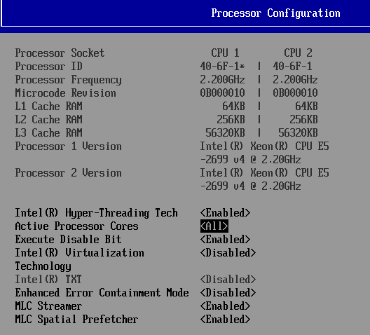
The typical BIOS settings can be seen below.
HP-G8 (2U Chassis) - Xeon E5-2690
| CPU | Two Intel Xeon processor E5-2690 (2.9GHz, 8c, 20MB L3, 135W) |
| RAM | 512 GB (16x32GB) Samsung DDR-3 LR-DIMM 1866 MHz @ 1333 MHz |
| Internal Disks | SAMSUNG MZ7LM240 (bootdisk) Intel SSD3700 800 GB (data) |
| Motherboard | HP G8 |
| BIOS version | 9/23/2016 |
| PSU | HP 750W (Gold) |
Other Notes
Both servers are fed by a standard European 230V (16 Amps max.) power line. The room temperature is monitored and kept at 23°C by our Airwell CRACs.
Memory Subsystem: Bandwidth
Measuring the full bandwidth potential with John McCalpin's Stream bandwidth benchmark is getting increasingly difficult on the latest CPUs, as core and memory channel counts have continued to grow. We compiled the stream 5.10 source code with the Intel compiler (icc) for linux version 17, or GCC 5.4, both 64-bit. The following compiler switches were used on icc:
icc -fast -qopenmp -parallel (-AVX) -DSTREAM_ARRAY_SIZE=800000000
Notice that we had to increase the array significantly, to a data size of around 6 GB. We compiled one version with AVX and one without.
The results are expressed in gigabytes per second.
Meanwhile the following compiler switches were used on gcc:
-Ofast -fopenmp -static -DSTREAM_ARRAY_SIZE=800000000
Notice that the DDR4 DRAM in the EPYC system ran at 2400 GT/s (8 channels), while the Intel system ran its DRAM at 2666 GT/s (6 channels). So the dual socket AMD system should theoretically get 307 GB per second (2.4 GT/s* 8 bytes per channel x 8 channels x 2 sockets). The Intel system has access to 256 GB per second (2.66 GT/s* 8 bytes per channel x 6 channels x 2 sockets).
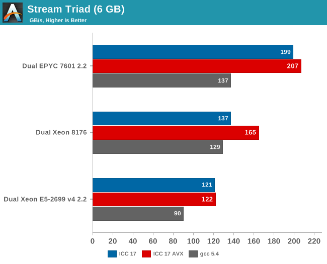
AMD told me they do not fully trust the results from the binaries compiled with ICC (and who can blame them?). Their own fully customized stream binary achieved 250 GB/s. Intel claims 199 GB/s for an AVX-512 optimized binary (Xeon E5-2699 v4: 128 GB/s with DDR-2400). Those kind of bandwidth numbers are only available to specially tuned AVX HPC binaries.
Our numbers are much more realistic, and show that given enough threads, the 8 channels of DDR4 give the AMD EPYC server a 25% to 45% bandwidth advantage. This is less relevant in most server applications, but a nice bonus in many sparse matrix HPC applications.
Maximum bandwidth is one thing, but that bandwidth must be available as soon as possible. To better understand the memory subsystem, we pinned the stream threads to different cores with numactl.
| Pinned Memory Bandwidth (in MB/sec) | |||
| Mem Hierarchy |
AMD "Naples" EPYC 7601 DDR4-2400 |
Intel "Skylake-SP" Xeon 8176 DDR4-2666 |
Intel "Broadwell-EP" Xeon E5-2699v4 DDR4-2400 |
| 1 Thread | 27490 | 12224 | 18555 |
| 2 Threads, same core same socket |
27663 | 14313 | 19043 |
| 2 Threads, different cores same socket |
29836 | 24462 | 37279 |
| 2 Threads, different socket | 54997 | 24387 | 37333 |
| 4 threads on the first 4 cores same socket |
29201 | 47986 | 53983 |
| 8 threads on the first 8 cores same socket |
32703 | 77884 | 61450 |
| 8 threads on different dies (core 0,4,8,12...) same socket |
98747 | 77880 | 61504 |
The new Skylake-SP offers mediocre bandwidth to a single thread: only 12 GB/s is available despite the use of fast DDR-4 2666. The Broadwell-EP delivers 50% more bandwidth with slower DDR4-2400. It is clear that Skylake-SP needs more threads to get the most of its available memory bandwidth.
Meanwhile a single thread on a Naples core can get 27,5 GB/s if necessary. This is very promissing, as this means that a single-threaded phase in an HPC application will get abundant bandwidth and run as fast as possible. But the total bandwidth that one whole quad core CCX can command is only 30 GB/s.
Overall, memory bandwidth on Intel's Skylake-SP Xeon behaves more linearly than on AMD's EPYC. All off the Xeon's cores have access to all the memory channels, so bandwidth more directly increases with the number of threads.
Memory Subsystem: Latency
The performance of modern CPUs depends heavily on the cache subsystem. And some applications depend heavily on the DRAM subsystem too. We used LMBench in an effort to try to measure cache and memory latency. The numbers we looked at were "Random load latency stride=16 Bytes".
| Mem Hierarchy |
AMD EPYC 7601 DDR4-2400 |
Intel Skylake-SP DDR4-2666 |
Intel Broadwell Xeon E5-2699v4 DDR4-2400 |
| L1 Cache cycles | 4 | 4 | 4 |
| L2 Cache cycles | 12 | 14-22 | 12-15 |
| L3 Cache 4-8 MB - cycles | 34-47 | 54-56 | 38-51 |
| 16-32 MB - ns | 89-95 ns | 25-27 ns (+/- 55 cycles?) |
27-42 ns (+/- 47 cycles) |
| Memory 384-512 MB - ns | 96-98 ns | 89-91 ns | 95 ns |
Previously, Ian has described the AMD Infinity Fabric that stitches the two CCXes together in one die and interconnects the 4 different "Zeppelin" dies in one MCM. The choice of using two CCXes in a single die is certainly not optimal for Naples. The local "inside the CCX" 8 MB L3-cache is accessed with very little latency. But once the core needs to access another L3-cache chunk – even on the same die – unloaded latency is pretty bad: it's only slightly better than the DRAM access latency. Accessing DRAM is on all modern CPUs a naturally high latency operation: signals have to travel from the memory controller over the memory bus, and the internal memory matrix of DDR4-2666 DRAM is only running at 333 MHz (hence the very high CAS latencies of DDR4). So it is surprising that accessing SRAM over an on-chip fabric requires so many cycles.
What does this mean to the end user? The 64 MB L3 on the spec sheet does not really exist. In fact even the 16 MB L3 on a single Zeppelin die consists of two 8 MB L3-caches. There is no cache that truly functions as single, unified L3-cache on the MCM; instead there are eight separate 8 MB L3-caches.
That will work out fine for applications that have a footprint that fits within a single 8 MB L3 slice, like virtual machines (JVM, Hypervisors based ones) and HPC/Big Data applications that work on separate chunks of data in parallel (for example, the "map" phase of "map/reduce"). However this kind of setup will definitely hurt the performance of applications that need "central" access to one big data pool, such as database applications and big data applications in the "Shuffle phase".
Memory Subsystem: TinyMemBench
To double check our latency measurements and get a deeper understanding of the respective architectures, we also use the open source TinyMemBench benchmark. The source was compiled for x86 with GCC 5.4 and the optimization level was set to "-O3". The measurement is described well by the manual of TinyMemBench:
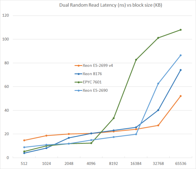
Average time is measured for random memory accesses in the buffers of different sizes. The larger the buffer, the more significant the relative contributions of TLB, L1/L2 cache misses, and DRAM accesses become. All the numbers represent extra time, which needs to be added to L1 cache latency (4 cycles).
We tested with dual random read, as we wanted to see how the memory system coped with multiple read requests.
L3-cache sizes have increased steadily over the years. The Xeon E5 v1 had up to 20 MB, v3 came with 45 MB, and v4 "Broadwell EP" further increased this to 55 MB. But the fatter the cache, the higher the latency became. L3 latency doubled from Sandy Bridge-EP to Broadwell-EP. So it is no wonder that Skylake went for a larger L2-cache and a smaller but faster L3. The L2-cache offers 4 times lower latency at 512 KB.
AMD's unloaded latency is very competitive under 8 MB, and is a vast improvement over previous AMD server CPUs. Unfortunately, accessing more 8 MB incurs worse latency than a Broadwell core accessing DRAM. Due to the slow L3-cache access, AMD's DRAM access is also the slowest. The importance of unloaded DRAM latency should of course not be exaggerated: in most applications most of the loads are done in the caches. Still, it is bad news for applications with pointer chasing or other latency-sensitive operations.
Single Threaded Integer Performance: SPEC CPU2006
Even in the server market where high core count CPUs are ruling the roost, high single threaded performance is still very desirable. It makes sure that a certain level of performance is guaranteed in every situation, not just in "throughput situations" of "embarrassingly parallel" software.
SPEC CPU2017 has finally launched, but it did so while our testing was already under way. So SPEC CPU2006 was still our best option to evaluate single threaded performance. Even though SPEC CPU2006 is more HPC and workstation oriented, it contains a good variety of integer workloads.
It is our conviction that we should try to mimic how performance critical software is compiled instead of trying to achieve the highest scores. To that end, we:
- use 64 bit gcc : by far the most used compiler on linux for integer workloads, good all round compiler that does not try to "break" benchmarks (libquantum...) or favor a certain architecture
- use gcc version 5.4: standard compiler with Ubuntu 16.04 LTS. (Note that this is upgraded from 4.8.4 used in earlier articles)
- use -Ofast -fno-strict-aliasing optimization: a good balance between performance and keeping things simple
- added "-std=gnu89" to the portability settings to resolve the issue that some tests will not compile with gcc 5.x
- run one copy of the test
The ultimate objective is to measure performance in non-"aggressively optimized" applications where for some reason – as is frequently the case – a "multi-thread unfriendly" task keeps us waiting.
First the single threaded results. It is important to note that thanks to modern turbo technology, all CPUs will run at higher clock speeds than their base clock speed.
- The Xeon E5-2690 ("Sandy Bridge") is capable of boosting up to 3.8 GHz
- The Xeon E5-2690 v3 ("Haswell") is capable of boosting up to 3.5GHz
- The Xeon E5-2699 v4 ("Broadwell") is capable of boosting up to 3.6 GHz
- The Xeon 8176 ("Skylake-SP") is capable of boosting up to 3.8 GHz
- The EPYC 7601 ("Naples") is capable of boosting up to 3.2 GHz
First we look at the absolute numbers.
| Subtest | Application type | Xeon E5-2690 @ 3.8 |
Xeon E5-2690 v3 @ 3.5 |
Xeon E5-2699 v4 @ 3.6 |
EPYC 7601 @3.2 |
Xeon 8176 @3.8 |
| 400.perlbench | Spam filter | 35 | 41.6 | 43.4 | 31.1 | 50.1 |
| 401.bzip2 | Compression | 24.5 | 24.0 | 23.9 | 24.0 | 27.1 |
| 403.gcc | Compiling | 33.8 | 35.5 | 23.7 | 35.1 | 24.5 |
| 429.mcf | Vehicle scheduling | 43.5 | 42.1 | 44.6 | 40.1 | 43.3 |
| 445.gobmk | Game AI | 27.9 | 27.8 | 28.7 | 24.3 | 31.0 |
| 456.hmmer | Protein seq. analyses | 26.5 | 28.0 | 32.3 | 27.9 | 35.4 |
| 458.sjeng | Chess | 28.9 | 31.0 | 33.0 | 23.8 | 33.6 |
| 462.libquantum | Quantum sim | 55.5 | 65.0 | 97.3 | 69.2 | 102 |
| 464.h264ref | Video encoding | 50.7 | 53.7 | 58.0 | 50.3 | 67.0 |
| 471.omnetpp | Network sim | 23.3 | 31.3 | 44.5 | 23.0 | 40.8 |
| 473.astar | Pathfinding | 25.3 | 25.1 | 26.1 | 19.5 | 27.4 |
| 483.xalancbmk | XML processing | 41.8 | 46.1 | 64.9 | 35.4 | 67.3 |
As raw SPEC scores can be a bit much to deal with in a dense table, we've also broken out our scores on a percentage basis. Sandy Bridge EP (Xeon E5 v1) is about 5 years old, the servers based upon this CPU are going to get replaced by newer ones. So we've made "Single threaded Sandy Bridge-EP performance" our reference (100%) , and compare the single threaded performance of all other architectures accordingly.
| Subtest | Application type | Xeon E5-2690 @ 3.8 |
Xeon E5-2690 v3 @ 3.5 |
Xeon E5-2699 v4 @ 3.6 | EPYC 7601 @3.2 | Xeon 8176 @ 3.8 |
| 400.perlbench | Spam filter | 100% | 119% | 124% | 89% | 143% |
| 401.bzip2 | Compression | 100% | 98% | 98% | 98% | 111% |
| 403.gcc | Compiling | 100% | 105% | 70% | 104% | 72% |
| 429.mcf | Vehicle scheduling | 100% | 97% | 103% | 92% | 100% |
| 445.gobmk | Game AI | 100% | 100% | 103% | 87% | 111% |
| 456.hmmer | Protein seq. analyses | 100% | 106% | 122% | 105% | 134% |
| 458.sjeng | Chess | 100% | 107% | 114% | 82% | 116% |
| 462.libquantum | Quantum sim | 100% | 117% | 175% | 125% | 184% |
| 464.h264ref | Video encoding | 100% | 106% | 114% | 99% | 132% |
| 471.omnetpp | Network sim | 100% | 134% | 191% | 99% | 175% |
| 473.astar | Pathfinding | 100% | 99% | 103% | 77% | 108% |
| 483.xalancbmk | XML processing | 100% | 110% | 155% | 85% | 161% |
SPEC CPU2006 analysis is complicated, and with only a few days spend on the EPYC server, we must admit that what follows is mostly educated guessing.
First off, let's gauge the IPC efficiency of the different architectures. Considering that the EPYC core runs at 12-16% lower clockspeeds (3.2 vs 3.6/3.8 GHz), getting 90+% of the performance of the Intel architectures can be considered a "strong" (IPC) showing for the AMD "Zen" architecture.
As for Intel's latest CPU, pay attention to the effect of the much larger L2-cache of the Skylake-SP core (Xeon 8176) compared to the previous generation "Broadwell". Especially perlbench, gobmk, hmmer and h264ref (the instruction part) benefit.
Meanwhile with the new GCC 5.4 compiler, Intel's performance on the "403.gcc benchmark" seems to have regressed their newer rchitectures. While we previously saw the Xeon E5-2699v4 perform at 83-95% of the "Sandy Bridge" Xeon E5-2690, this has further regressed to 70%. The AMD Zen core, on the other hand, does exceptionally well when running GCC. The mix of a high percentage of (easy to predict) branches in the instruction mix, a relatively small footprint, and a heavy reliance on low latency (mostly L1/L2/8 MB L3) seems to work well. The workloads where the impact of branch prediction is higher (somewhat higher percentage of branch misses) - gobmk, sjeng, hmmer - perform quite well on "Zen" too, which has a much lower branch misprediction penalty than AMD's previous generation architecture thanks to the µop cache.
Otherwise the pointer chasing benchmarks – XML procesing and Path finding – which need a large L3-cache, are the worst performing on EPYC.
Also notice the fact that the low IPC omnetpp ("network sim") runs slower on Skylake-SP than on Broadwell, but still much faster than AMD's EPYC. Omnetpp is an application that benefited from the massive 55 MB L3-cache of Broadwell, and that is why performance has declined on Skylake. Of course, this also means that the fractured 8x8 MB L3 of AMD's EPYC processor causes it to perform much slower than the latest Intel server CPUs. In the video encoding benchmark "h264ref" this plays a role too, but that benchmark relies much more on DRAM bandwidth. The fact that the EPYC core has higher DRAM bandwidth available makes sure that the AMD chip does not fall too far behind the latest Intel cores.
All in all, we think we can conclude that the single threaded performance of the "Zen architecture" is excellent, but it somewhat let down by the lower turbo clock and the "smaller" 8x8 MB L3-cache.
SMT Integer Performance With SPEC CPU2006
Next, to test the performance impact of simultaneous multithreading (SMT) on a single core, we test with two threads on the same core. This way we can evaluate how well the core handles SMT.
| Subtest | Application type | Xeon E5-2690 @ 3.8 | Xeon E5-2690 v3 @ 3.5 | Xeon E5-2699 v4 @ 3.6 | EPYC 7601 @3.2 | Xeon 8176 @ 3.8 |
| 400.perlbench | Spam filter | 39.8 | 43.9 | 47.2 | 40.6 | 55.2 |
| 401.bzip2 | Compression | 32.6 | 32.3 | 32.8 | 33.9 | 34.8 |
| 403.gcc | Compiling | 40.7 | 43.8 | 32.5 | 41.6 | 32.1 |
| 429.mcf | Vehicle scheduling | 44.7 | 51.3 | 55.8 | 44.2 | 56.6 |
| 445.gobmk | Game AI | 36.6 | 35.9 | 38.1 | 36.4 | 39.4 |
| 456.hmmer | Protein seq. analyses | 32.5 | 34.1 | 40.9 | 34.9 | 44.3 |
| 458.sjeng | Chess | 36.4 | 36.9 | 39.5 | 36 | 41.9 |
| 462.libquantum | Quantum sim | 75 | 73.4 | 89 | 89.2 | 91.7 |
| 464.h264ref | Video encoding | 52.4 | 58.2 | 58.5 | 56.1 | 75.3 |
| 471.omnetpp | Network sim | 25.4 | 30.4 | 48.5 | 26.6 | 42.1 |
| 473.astar | Pathfinding | 31.4 | 33.6 | 36.6 | 29 | 37.5 |
| 483.xalancbmk | XML processing | 43.7 | 53.7 | 78.2 | 37.8 | 78 |
Now on a percentage basis versus the single-threaded results, so that we can see how much performance we gained from enabling SMT:
| Subtest | Application type | Xeon E5-2699 v4 @ 3.6 | EPYC 7601 @3.2 | Xeon 8176 @ 3.8 |
| 400.perlbench | Spam filter | 109% | 131% | 110% |
| 401.bzip2 | Compression | 137% | 141% | 128% |
| 403.gcc | Compiling | 137% | 119% | 131% |
| 429.mcf | Vehicle scheduling | 125% | 110% | 131% |
| 445.gobmk | Game AI | 125% | 150% | 127% |
| 456.hmmer | Protein seq. analyses | 127% | 125% | 125% |
| 458.sjeng | Chess | 120% | 151% | 125% |
| 462.libquantum | Quantum sim | 91% | 129% | 90% |
| 464.h264ref | Video encoding | 101% | 112% | 112% |
| 471.omnetpp | Network sim | 109% | 116% | 103% |
| 473.astar | Pathfinding | 140% | 149% | 137% |
| 483.xalancbmk | XML processing | 120% | 107% | 116% |
On average, both Xeons pick up about 20% due to SMT (Hyperthreading). The EPYC 7601 improved by even more: it gets a 28% boost on average. There are many possible explanations for this, but two are the most likely. In the situation where AMD's single threaded IPC is very low because it is waiting on the high latency of a further away L3-cache (>8 MB), a second thread makes sure that the CPU resources can be put to better use (like compression, the network sim). Secondly, we saw that AMD core is capable of extracting more memory bandwidth in lightly threaded scenarios. This might help in the benchmarks that stress the DRAM (like video encoding, quantum sim).
Nevertheless, kudos to the AMD engineers. Their first SMT implementation is very well done and offers a tangible throughput increase.
Multi-core SPEC CPU2006
For the record, we do not believe that the SPEC CPU "Rate" metric has much value for estimating server CPU performance. Most applications do not run lots of completely separate processes in parallel; there is at least some interaction between the threads. But since the benchmark below caused so much discussion, we wanted to satisfy the curiosity of our readers.
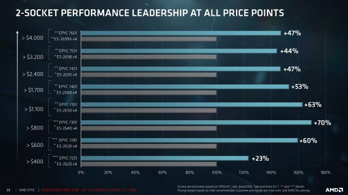
Does the EPYC7601 really have 47% more raw integer power? Let us find out. Though please note that you are looking at officially invalid base SPEC rate runs, as we still have to figure out how to tell the SPEC software that our "invalid" flag "-Ofast" is not invalid at all. We did the required 3 iterations though.
| Subtest | Application type | Xeon E5-2699 v4 @ 2.8 |
Xeon 8176 @ 2.8 |
EPYC 7601 @2.7 |
EPYC Vs Broadwell EP |
EPYC vs Skylake SP |
| 400.perlbench | Spam filter | 1470 | 1980 | 2020 | +37% | +2% |
| 401.bzip2 | Compression | 860 | 1120 | 1280 | +49% | +14% |
| 403.gcc | Compiling | 960 | 1300 | 1400 | +46% | +8% |
| 429.mcf | Vehicle scheduling | 752 | 927 | 837 | +11% | -10% |
| 445.gobmk | Game AI | 1220 | 1500 | 1780 | +46% | +19% |
| 456.hmmer | Protein seq. analyses | 1220 | 1580 | 1700 | +39% | +8% |
| 458.sjeng | Chess | 1290 | 1570 | 1820 | +41% | +16% |
| 462.libquantum | Quantum sim | 545 | 870 | 1060 | +94% | +22% |
| 464.h264ref | Video encoding | 1790 | 2670 | 2680 | +50% | -0% |
| 471.omnetpp | Network sim | 625 | 756 | 705 (*) | +13% | -7% |
| 473.astar | Pathfinding | 749 | 976 | 1080 | +44% | +11% |
| 483.xalancbmk | XML processing | 1120 | 1310 | 1240 | +11% | -5% |
(*) We had to run 471.omnetpp with 64 threads on EPYC: when running at 128 threads, it gave errors. Once solved, we expect performance to be 10-20% higher.
Ok, first a disclaimer. The SPECint rate test is likely unrealistic. If you start up 88 to 128 instances, you create a massive bandwidth bottleneck and a consistent CPU load of 100%, neither of which are very realistic in most integer applications. You have no synchronization going on, so this is really the ideal case for a processor such as the AMD EPYC 7601. The rate test estimates more or less the peak integer crunching power available, ignoring many subtle scaling problems that most integer applications have.
Nevertheless, AMD's claim was not farfetched. On average, and using a "neutral" compiler with reasonable compiler settings, the AMD 7601 has about 40% (42% if you take into account that our Omnetpp score will be higher once we fixed the 128 instances issue) more "raw" integer processing power than the Xeon E5-2699 v4, and is even about 6% faster than the Xeon 8176. Don't expect those numbers to be reached in most real integer applications though. But it shows how much progress AMD has made nevertheless...
Multi-Threaded Integer Performance
While stand-alone compression and decompression are not real world benchmarks in and of themselves (at least as far as servers go), more and more servers have to perform these tasks as part of a larger role (e.g. database compression, website optimization).
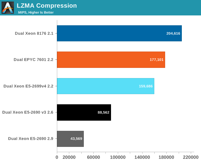
Compression relies a lot on cache, memory latency, and TLB efficiency. This is definitely not the ideal situation for AMD's EPYC CPU. The best AMD CPU has almost 50% more cores than the previous Intel Xeon, but delivers only 11% more performance.
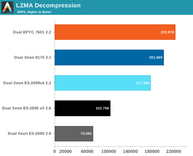
Decompression relies on less common integer instructions (shift, multiply). Intel and AMD cores seems to handle these integer instructions similarly, but AMD's chip has 4 cores more. Fourteen percent more cores result in about 10% faster decompression performance.
Database Performance: MySQL Percona Server 5.7.0
For database benchmarking we still base our testing on Percona server 5.7, an enhanced drop-in replacement for MySQL. But we have updated our SQL benchmarking once again. This time we use Sysbench 1.0.7, which is a lot more efficient than the previous 0.4 and 0.5 versions. As a result, the measured numbers are quite a bit higher, especially on the strongest systems. So you cannot compare this with any similar Sysbench-based benchmarking we have done before.
For our testing we used the read-only OLTP benchmark, which is slightly less realistic, but still much more interesting than most other Sysbench tests. This allows us to measure CPU performance without creating an I/O bottleneck.
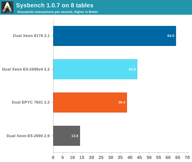
As expected, the EPYC 7601 can not deliver high database performance out of the box. A small database that can be mostly cached in the L3-cache is the worst case scenario for EPYC. That said, there are quite a few tuning opportunities on EPYC. According to AMD, if you enable Memory Interleaving, performance should rise a bit (+10-15%?). Unfortunately, a few days before our deadline our connection to the BMC failed, so we could not try it out. In a later article, we will go deeper into specific tuning for both platforms and test additional database systems.
Nevertheless, our point stands: out of the box is the EPYC CPU a rather mediocre transactional database CPU. With good tuning it is possible EPYC may pass the Xeon v4, but the 8176 is by far the champion here. It will be interesting to measure how EPYC compares in the non-transactional databases (Document stores, Key-value...) but transactional databases will remain Intel territory for now.
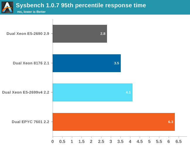
Typically when high response times were reported, this indicated low single threaded performance. However for EPYC this is not the case. We tested with a database that is quite a bit larger than the 8 MB L3-cache, and the high response time is probably a result of the L3-cache latency.
Java Performance
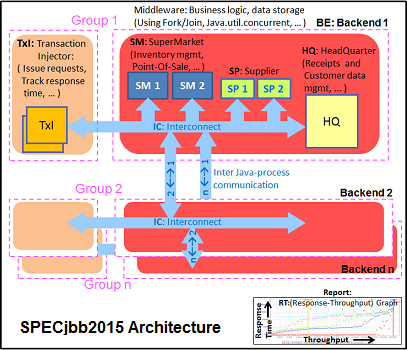
The SPECjbb 2015 benchmark has "a usage model based on a world-wide supermarket company with an IT infrastructure that handles a mix of point-of-sale requests, online purchases, and data-mining operations." It uses the latest Java 7 features and makes use of XML, compressed communication, and messaging with security.
We tested SPECjbb with four groups of transaction injectors and backends. The reason why we use the "Multi JVM" test is that it is more realistic: multiple VMs on a server is a very common practice.
The Java version was OpenJDK 1.8.0_131. We applied relatively basic tuning to mimic real-world use, while aiming to fit everything inside a server with 128 GB of RAM:
The graph below shows the maximum throughput numbers for our MultiJVM SPECJbb test.
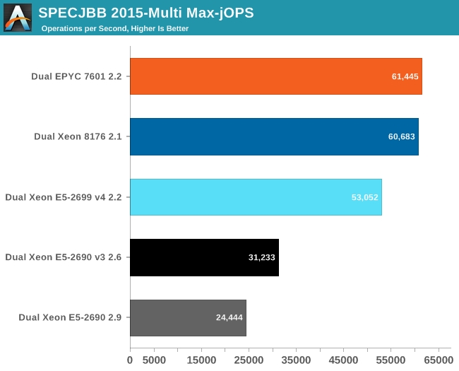
Even though our testing is not the ideal case for AMD (you would probably choose 8 or even 16 back-ends), the EPYC edges out the Xeon 8176. Using 8 JVMs increases the gap from 1% to 4-5%.
The Critical-jOPS metric is a throughput metric under response time constraint.
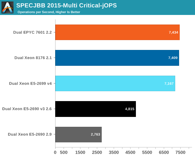
With this number of threads active, you can get much higher Critical-jOps by significantly increasing the RAM per JVM. However, we did not want that as this would mean we can not compare with systems that can only accommodate 128 GB of RAM.
Apache Spark 2.1 Benchmarking
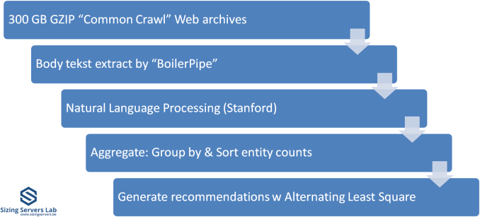
Apache Spark is the poster child of Big Data processing. Speeding up Big Data applications is the top priority project at the university lab I work for (Sizing Servers Lab of the University College of West-Flanders), so we produced a benchmark that uses many of the Spark features and is based upon real world usage.
The test is described in the graph above. We first start with 300 GB of compressed data gathered from the CommonCrawl. These compressed files are a large amount of web archives. We decompress the data on the fly to avoid a long wait that is mostly storage related. We then extract the meaningful text data out of the archives by using the Java library "BoilerPipe". Using the Stanford CoreNLP Natural Language Processing Toolkit, we extract entities ("words that mean something") out of the text, and then count which URLs have the highest occurrence of these entities. The Alternating Least Square algorithm is then used to recommend which URLs are the most interesting for a certain subject.
In previous articles, we tested with Spark 1.5 in standalone mode (non-clustered). That worked out well enough, but we saw diminishing returns as core counts went up. In hindsight, just dumping 300 GB of compressed data in one JVM was not optimal for 30+ core systems. The high core counts of the Xeon 8176 and EPYC 7601 caused serious performance issues when we first continued to test this way. The 64 core EPYC 7601 performed like a 16-core Xeon, the Skylake-SP system with 56 cores was hardly better than a 24-core Xeon E5 v4.
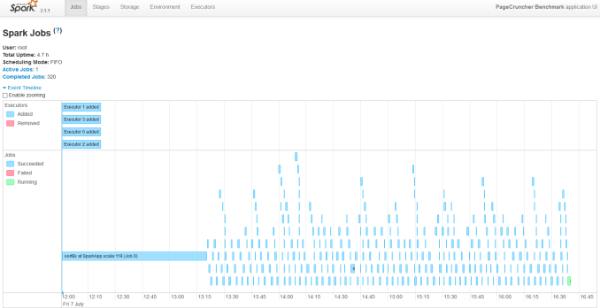
So we decided to turn our newest servers into virtual clusters. Our first attempt is to run with 4 executors. Researcher Esli Heyvaert also upgraded our Spark benchmark so it could run on the latest and greatest version: Apache Spark 2.1.1.
Here are the results:
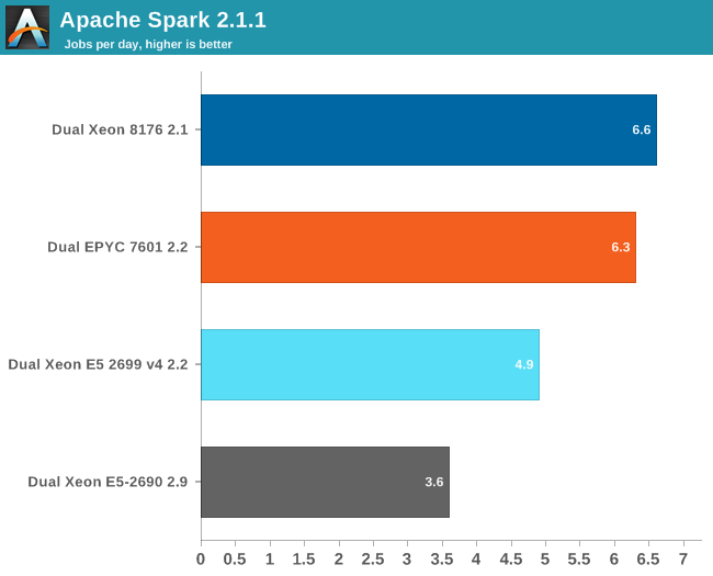
If you wonder who needs such server behemoths besides the people who virtualize a few dozen virtual machines, the answer is Big Data. Big Data crunching has an unsatisfiable hunger for – mostly integer – processing power. Even on our fastest machine, this test needs about 4 hours to finish. It is nothing less than a killer app.
Our Spark benchmark needs about 120 GB of RAM to run. The time spent on storage I/O is negligible. Data processing is very parallel, but the shuffle phases require a lot of memory interaction. The ALS phase does not scale well over many threads, but is less than 4% of the total testing time.
Given the higher clockspeed in lightly threaded and single threaded parts, the faster shuffle phase probably gives the Intel chip an edge of only about 5%.
Floating Point
Normally our HPC benchmarking is centered around OpenFoam, a CFD software we have used for a number of articles over the years. However, since we moved to Ubuntu 16.04, we could not get it to work anymore. So we decided to change our floating point intensive benchmark for now. For our latest article, we're testing with C-ray, POV-Ray, and NAMD.
The idea is to measure:
- A FP benchmark that is running out of the L1 (C-ray)
- A FP benchmark that is running out of the L2 (POV-Ray)
- And one that is using the memory subsytem quite often (NAMD)
Floating Point: C-ray
C-ray is an extremely simple ray-tracer which is not representative of any real world raytracing application. In fact, it is essentially a floating point benchmark that runs out of the L1-cache. Luckily it is not as synthetic and meaningless as Whetstone, as you can actually use the software to do simple raytracing.
We use the standard benchmarking resolution (3840x2160) and the "sphfract" file to measure performance. The binary was precompiled.
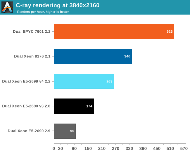
Wow. What just happened? It looks like a landslide victory for the raw power of the four FP pipes of Zen: the EPYC chip is no less than 50% faster than the competition. Of course, it is easy to feed FP units if everything resides in the L1. Next stop, POV-Ray.
Floating Point: POV-Ray 3.7
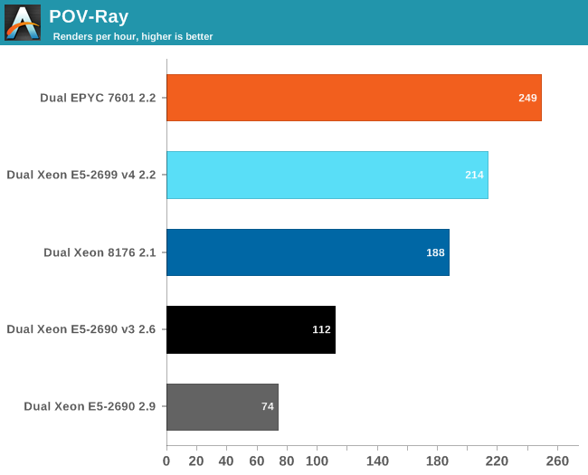
POV-Ray is known to run mostly out of the L2-cache, so the massive DRAM bandwidth of the EPYC CPU does not play a role here. Nevertheless, the EPYC CPU performance is pretty stunning: about 16% faster than Intel's Xeon 8176. But what if AVX and DRAM access come in to play? Let us check out NAMD.
Floating Point: NAMD
Developed by the Theoretical and Computational Biophysics Group at the University of Illinois Urbana-Champaign, NAMD is a set of parallel molecular dynamics codes for extreme parallelization on thousands of cores. NAMD is also part of SPEC CPU2006 FP. In contrast with previous FP benchmarks, the NAMD binary is compiled with Intel ICC and optimized for AVX.
First, we used the "NAMD_2.10_Linux-x86_64-multicore" binary. We used the most popular benchmark load, apoa1 (Apolipoprotein A1). The results are expressed in simulated nanoseconds per wall-clock day. We measure at 500 steps.
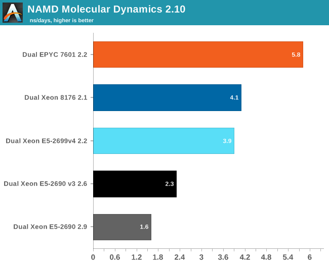
Again, the EPYC 7601 simply crushes the competition with 41% better performance than Intel's 28-core. Heavily vectorized code (like Linpack) might run much faster on Intel, but other FP code seems to run faster on AMD's newest FPU.
For our first shot with this benchmark, we used version 2.10 to be able to compare to our older data set. Version 2.12 seems to make better use of "Intel's compiler vectorization and auto-dispatch has improved performance for Intel processors supporting AVX instructions". So let's try again:
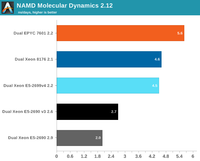
The older Xeons see a perforance boost of about 25%. The improvement on the new Xeons is a lot lower: about 13-15%. Remarkable is that the new binary is slower on the EPYC 7601: about 4%. That simply begs for more investigation: but the deadline was too close. Nevertheless, three different FP tests all point in the same direction: the Zen FP unit might not have the highest "peak FLOPs" in theory, there is lots of FP code out there that runs best on EPYC.
Energy Consumption
We tested the energy consumption of our servers for a one-minute period in several scenario. The first scenario is the point where the server under testing performs best in MySQL: the highest throughput just before the response time goes up significantly.
To test the power usage of the FPU, we measure the power consumption when POV-Ray was using all available threads.
| SKU | TDP (on paper) spec |
Idle Server W |
MySQL Best Throughput at Lowest Resp. Time (*) (W) |
POV-Ray 100% CPU load |
| Dual Xeon E5-2699 v4 | 2x145 W | 106 | 412 | 425 |
| Dual Xeon 8176 | 2x165W | 190 | 300 | 453 |
| Dual EPYC 7601 | 2x180W | 151 | 321 | 327 |
Both the Xeon 8176 and Dual EPYC server had a few more additional components (a separate 10 GBe card for example) than the Dual Xeon E5-2699v4 system, but that does not fully explain why idle power is so much higher, especially on the Dual Xeon 8176. We lacked the time to fully investigate this, and the last two systems have relatively new firmware.
The only conclusion that we can draw so far, is that the EPYC 7601 is likely to draw more power when running integer applications, while the rather wide FP units of the Intel CPUs are real power hogs even if they do not run heavy AVX applications. To be continued...
Closing Thoughts
First of all, we have to emphasize that we were only able to spend about a week on the AMD server, and about two weeks on the Intel system. With the complexity of both server hardware and especially server software, that is very little time. There is still a lot to test and tune, but the general picture is clear.
We can continue to talk about Intel's excellent mesh topology and AMD strong new Zen architecture, but at the end of the day, the "how" will not matter to infrastructure professionals. Depending on your situation, performance, performance-per-watt, and/or performance-per-dollar are what matters.
The current Intel pricing draws the first line. If performance-per-dollar matters to you, AMD's EPYC pricing is very competitive for a wide range of software applications. With the exception of database software and vectorizable HPC code, AMD's EPYC 7601 ($4200) offers slightly less or slightly better performance than Intel's Xeon 8176 ($8000+). However the real competitor is probably the Xeon 8160, which has 4 (-14%) fewer cores and slightly lower turbo clocks (-100 or -200 MHz). We expect that this CPU will likely offer 15% lower performance, and yet it still costs about $500 more ($4700) than the best EPYC. Of course, everything will depend on the final server system price, but it looks like AMD's new EPYC will put some serious performance-per-dollar pressure on the Intel line.
The Intel chip is indeed able to scale up in 8 sockets systems, but frankly that market is shrinking fast, and dual socket buyers could not care less.
Meanwhile, although we have yet to test it, AMD's single socket offering looks even more attractive. We estimate that a single EPYC 7551P would indeed outperform many of the dual Silver Xeon solutions. Overall the single-socket EPYC gives you about 8 cores more at similar clockspeeds than the 2P Intel, and AMD doesn't require explicit cross socket communication - the server board gets simpler and thus cheaper. For price conscious server buyers, this is an excellent option.
However, if your software is expensive, everything changes. In that case, you care less about the heavy price tags of the Platinum Xeons. For those scenarios, Intel's Skylake-EP Xeons deliver the highest single threaded performance (courtesy of the 3.8 GHz turbo clock), high throughput without much (hardware) tuning, and server managers get the reassurance of Intel's reliable track record. And if you use expensive HPC software, you will probably get the benefits of Intel's beefy AVX 2.0 and/or AVX-512 implementations.
The second consideration is the type of buyer. It is clear that you have to tune more and work harder to get the best performance out of AMD EPYC CPUs. In many ways it is basically a "virtual octal socket" solution. For enterprises with a small infrastructure crew and server hardware on premise, spending time on hardware tuning is not an option most of the time. For the cloud vendors, the knowledge will be available and tuning for EPYC will be a one-time investment. Microsoft is already deploying AMD's EPYC in their Azure Cloud Datacenters.
Looking Towards the Future
Looking towards the future, Intel has the better topology to add more cores in future CPU generations. However AMD's newest core is a formidable opponent. Scalar floating point operations are clearly faster on the AMD core, and integer performance is – at the same clock – on par with Intel's best. The dual CCX layout and quad die setup leave quite a bit of performance on the table, so it will be interesting how much AMD has learned from this when they launch the 7 nm "Rome" successor. Their SKU line-up is still very limited.
All in all, it must be said that AMD executed very well and delivered a new server CPU that can offer competitive performance for a lower price point in some key markets. Server customers with non-scalar sparse matrix HPC and Big Data applications should especially take notice.
As for Intel, the company has delivered a very attractive and well scaling product. But some of the technological advances in Skylake-SP are overshadowed by the heavy price tags and somewhat "over the top" market segmentation.

