Original Link: https://www.anandtech.com/show/1132
DFI 748-AL: First Look at SiS 748
by Wesley Fink on August 30, 2003 12:00 AM EST- Posted in
- Motherboards
You can’t look at a SiS chipset board these days without asking, “what is happening to SiS?” After the heady days of growth in the Intel market, SiS has grown strangely quiet. The phenomenal growth that started with the SiS 645 chipset and progressed through the SiS 645DX, SiS 648, and finally the dual-channel SiS 655 seems to have stopped. The forays into Athlon country with the 700 series chipsets (735/746/746FX) seem to have lost all their steam since nVidia began their takeover of the AMD market. Even the long-rumored 800FSB Dual-Channel SiS 655FX chipset for Pentium 4 has turned into an endless series of delay announcements while SiS market share continues to dwindle. It wasn’t long ago that SiS was poised to pass VIA as the top chipset maker in Taiwan, but now both SiS and VIA seem to have fallen on hard times. There are many questions, more rumors, and very few hard facts. We don’t have answers to these questions.
It was in this climate that we first began to hear of a new SiS 748 chipset for Athlon, but honestly, you had to strain to even hear rumors. The new SiS 748 chipset for Athlon is as difficult to find as the proverbial needle-in-a-haystack. The first 748 that we were aware of was produced by long-term SiS partner, iWill. But early reports on that board indicated almost none of the overclocking options that iWill had lavished on their earlier SiS Athlon motherboards. There were also reports of an Asrock version of the 748 at the very low end with almost no tweaking options. Asrock is the ASUS division that produces low-end value boards. It appeared that the 748 was already destined to be the “bargain-bargain” chipset of the Athlon world, slated below even the glut of KT600 boards that are being targeted at the “value” segment.
Then we began hearing about a 748 board that would be produced by DFI that was not a fancy LANParty board, yet had many of the tweaking and overclocking options which were missing from the SiS 748 boards that we had seen. We asked DFI if we could take a look at their SiS 748 board, called the DFI 748-AL, and DFI San Jose graciously had an engineering sample in our hands in just a couple of days. We were warned that this was a value board, and not in the same league as their LANParty series, but that didn’t dampen our enthusiasm. DFI is a major OEM manufacturer — they make many boards for other companies — and we had always found their mainstream boards solid and stable, if not the most exciting on the market.
As stated before, there is no inherent reason why a dual-channel chipset would be the performance leader on the AMD Athlon platform. Due to the limitations of the Athlon architecture, single-channel solutions should be able to compete effectively in most performance areas with the dual-channel nForce2 Ultra 400. Recently, the single-channel nForce2 400 has proven that this is more than just a theory. We’ve already seen that KT-600 is not likely the killer single-channel solution that we expected. So, could the SiS 748 be the solution that finally stands head-to-head with nForce2?
The interest in the DFI 748-AL was to try to answer this question. Does the SiS 748 chipset have any potential? Or will it be so out-performed and overshadowed by the nForce2 Ultra 400/400 and VIA KT600 juggernaut that it will die before it is even launched? We hope to be able to shed some light on those questions in this review.
SiS 748/963L Chipset
The SiS 748/963L chipset is the latest in the SiS 700 series chipsets for AMD Athlon processors. 748 adds full support for the latest 200FSB Athlon CPUs, such as the Barton 3200+. The 748 chipset also features technology, called “Hyperstreaming Engine”, which SiS claims makes their Single-Channel Memory solution as fast as Dual-Channel Athlon solutions.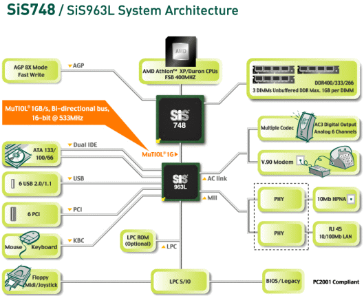
Click image to view a larger picture.
Hyperstreaming uses a number of techniques to manage data flow through the entire computer – all designed with the goal of reducing wait states and improving performance of the computer system. Hyperstreaming Engine optimizes performance using these techniques:
1. Low Latency with single streamYou can read more about the SiS Hyperstreaming Engine at www.sis.com/hyperstreaming/index.htm. Sis also includes a number of charts, comparing the Hyperstreaming Engine to “V Corporation” and “N Corporation”. All of the combined Hyperstreaming features are designed to remove data bottlenecks and to improve I/O intensive operations, like copying and downloading files from the internet.
2. Pipelining and Concurrent Execution with Multiple streams
3. “Prioritized Channel” with Specific stream
4. “Smart flow control” and “Intelligent arbitration” with Smart stream
The other innovation in the 748/963L chipset is the 1GHz “Mutiol” bus used to communicate between the north and south bridges. This should also improve performance of the chipset.
DFI 748-AL: Basic Features
| Motherboard Specifications | |
| CPU Interface | Socket-462 |
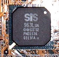
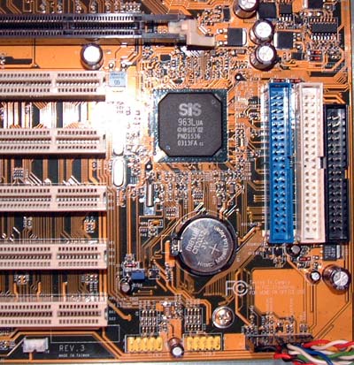
| Chipset | SiS 748 North Bridge SiS 963L South Bridge |
| Bus Speeds | up to 232MHz (in 1MHz increments) |
| Core Voltages Supported | up to 1.850V (in 0.025V increments) |
| AGP Voltages Supported | up to 1.8V (in 0.1V increments) |
| DRAM Voltages Supported | up to 2.8V (in 0.1V increments) |
| Chipset Voltage | 1.8V to 2.1V in 0.1V increments |
| CPU Multiplier Ratios | 5X to 21X |
| Memory Slots | 3 x 184-pin DDR DIMM Slots |
| Expansion Slots | 1 AGP 8X Slot 5 PCI Slots |
| Onboard IDE RAID | Standard ATA 133/100/66 Supporting up to 4 IDE devices |
| Onboard USB 2.0/IEEE-1394 | 6 USB 2.0 ports supported by 964L No FireWire |
| Onboard LAN | SiS 900 10/100 LAN |
| Onboard Audio | AC'97 2.2 compliant 5.1 codec |
| Onboard Serial ATA | None |
| BIOS Revision | Evaluation BIOS (8/08/2003) |
The DFI 748-AL is a good example of how much has been added to motherboard features in the last few years. With on-board 10/100 LAN, 5.1 channel audio, 6 USB 2.0 ports, ATA133 IDE support, and 8X AGP, the 748-AL would have been considered loaded just a short time ago. Now, compared to the feature-rich boards in the market, it is considered a standard or value board. Nothing you really need is absent from the 748 unless you need firewire, and that can be added with an add-on card.
Since our test board was an Engineering Sample, we cannot be sure exactly what accessories will ship with the release 748-AL, but we would suspect you will receive IDE cables, floppy cable, a CD with drivers, possibly a USB bracket, and not much else. You shouldn’t expect more than basics with a board designed to sell for a value price.
The DFI is anything but a value board in the tweaking and overclocking options. The ranges DFI has provided are the best we have seen on any announced SiS 748 motherboard. It is also the only 748 to provide CPU multiplier selection in BIOS — an important feature for many AMD users.
DFI has included an AC’97 compliant 6-channel audio on the 748-AL. Specifications on the website show a Realtek codec used, but our Engineering Sample was equipped with the cMedia codec used on the LANParty series. Both the Realtek and cMedia are AC’97 complaint, so either would meet specifications. There is also a connector for an optional SPDIF bracket.
On-board LAN is provided by SiS 900 Ethernet code in the 963L southbridge. The SiS 900 is a 10/100 Ethernet connection.
DFI has included 2 USB 2.0 ports on the I/O panel with headers for 4 additional USB 2 ports on the motherboard, for a total of 6 USB 2.0 ports provided by the 748/963L chipset. With SiS, VIA, and nVidia all providing extensive USB 2.0 support in their latest chipsets, this has become a standard feature.
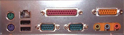
The 748-AL uses the standard ATX ports configuration and can be used with the standard plates that come with ATX cases. This includes PS/2 mouse and keyboard ports, two USB 2.0 ports, one 10/100 LAN port, two serial ports, one parallel port, game port, and Mic In, Line In, and Line Out, which are controlled by the onboard sound. There are no Firewire ports.
Sis has been a pioneer in high-speed links between north and south bridges, and we find the 1GB Mutiol connection used on the 748-AL. Hyperstreaming, which was discussed in our look at the 748 chipset, is also a feature of the 748/963L chipset. Both are features designed to improve speed of the motherboard.
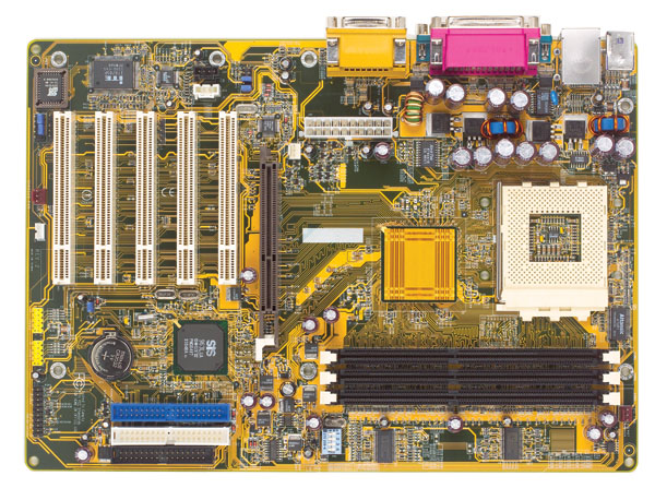
DFI 748-AL: Board Layout
Click image to view a larger picture.
The DFI 748-AL is a less than full-size board, which we often see in boards designed to sell at lower prices, but it does not feel cramped in any way. 7 standoffs are used to mount the board to the case. It generally has a good layout, especially considering the smaller size of the board, and the price it is selling for.
Click image to view a larger picture.
One location we are particular about is the ATX (20-pin) connector position, because the cable is very bulky and difficult to connect if poorly placed. The 748-AL ATX connector is located near the midline of the PCB to the left of the CPU socket. This is a common place for the ATX connector, but it is one of worst locations possible for the end-user. This means you have to snake the bulky 20-pin cable either around your CPU or over it. This location can also obstruct the installation/uninstallation of the CPU, CPU HSF, and possibly memory modules, depending on case design. We prefer a right of CPU upper position for the 20-pin connector, since this works well in most case designs. There is not an additional 4-pin 12V connector on the 748-AL. This optional power connection is starting to appear on many Athlon boards, but is not used on the 748-AL. The SiS 748 reference board did not use the 4-pin 12V either, so it’s not likely the 4-pin 12V will be seen on any 748 boards.
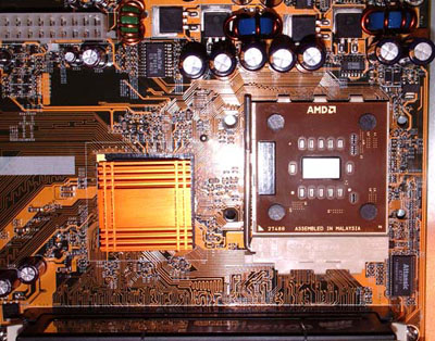
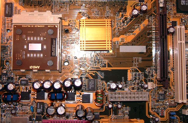
The space around the CPU and north bridge is very important if you plan to mount larger heatsink/fans or water-cooling solutions. As you can see, DFI has kept this area clean and clear on the 748-AL. It’s also a pleasant surprise to find the 4 holes around the CPU for large heavy HSFs from Alpha, Swiftech, Thermalright, OCZ and others. Fans of water-cooling will also be pleased to see the 4 holes for mounting some of the water-block solutions.
The 3 dimm sockets support the maximum 3GB available with the SiS 748 chipset. The arrangement on the DFI 748-AL is also excellent, making it very easy to add and remove memory without having to remove your video card. There is very little to complain about in the arrangement of this area.
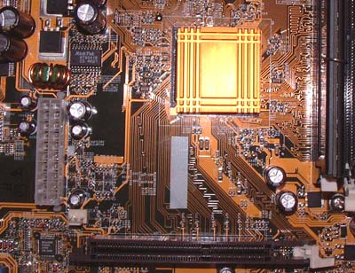
As often seen on boards designed to sell at a low price, the north bridge heatsink is shallow and small. While it was perfectly adequate for normal operation, we found that the north bridge became very warm in the large overclocks possible with this board. This caused us some problems in our overclock stress testing. If this board will be used for squeezing performance from your Athlon, then we would suggest you replace the stock north bridge with a more effective passive or active cooling solution. There is a 3rd fan header, colored white, near the 20-pin ATX connector for active solutions, but you will have to watch weight as the north bridge cooler must be mounted with tape or thermal epoxy.
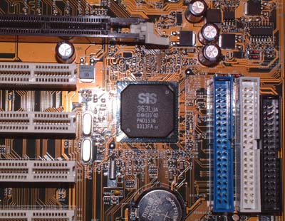
One problem with smaller boards is it is usually impossible to place the IDE connectors and Floppy connectors in the best upper right location behind the dimm sockets. Considering the available options, DFI has wisely place the IDE/Floppy connectors just below mid and to the right of the board. Some thought went into this, because the connectors are completely clear of the AGP 8X slot, and some of the largest cards you will see in today’s designs are video cards. The Primary and Secondary IDE connectors are, in our opinion, best located above the midsection of the motherboard and to the right of the DIMM slots, which allows the standard bundled IDE cables to reach the upper bays of an ATX case. This means you will be able to install optical drives in the 1st and 2nd bays. This location also allows better air flow and case organization to be possible and allows the user to make use of the Slave connector on the bundled IDE cables. While the 748-AL does not use the ideal position, the IDE/Floppy connectors are in a good location considering the options available.
The DFI 748-AL floppy connection is placed with the IDE connectors to the far right just below midline. This location might be a challenge for case designs with the floppy drive at the top of the case, but it should work fine for most case arrangements. At least we don’t find a floppy connector at the bottom of the board, which is often a nightmare.
![]()
The DFI 748-AL has 5 PCI slots for expansion cards and an 8X AGP slot. Considering the options already on board the 748-AL and the mainstream market it will sell to, this should be plenty of expansion options. The AGP/PCI slots are well arranged and are clear of the 3 Dimm slots. There is plenty of room for adding and removing memory modules without interfering with the AGP card.
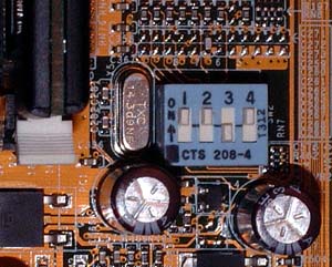
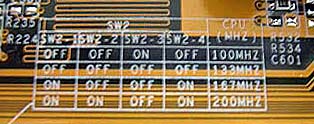
Almost every motherboard these days defaults to automatic CPU setup. This can be useful, but it can also be a handicap if, for instance, you have a Barton 2500+ that runs just fine as a 3200+ at default voltage. DFI considered that possibility with the 748-AL, and you can go with default CPU settings or force 100,133,166, or 200FSB with a Dip switch. Settings for the switch are silk-screened on the motherboard.
DFI 748-AL: BIOS and Overclocking
DFI uses the familiar Award BIOS for the 748-AL. The BIOS is the first “Performance” BIOS that we have seen used on a SiS 748 board, and the overclocking options are very complete for a board designed to sell for a low price.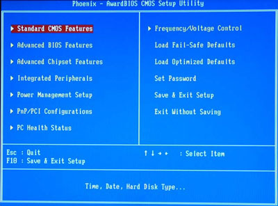
The Main BIOS Screen layout includes the standard options plus selections for Frequency/Voltage Control, Advanced Chipset Features for system timings, and PC Health Status.
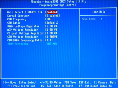
CPU FSB and multiplier ratios are adjusted in the Frequency/Voltage Control menu. Voltage adjustments are included for Core Voltage, Memory, AGP, and chipset voltage. This is a very complete set of controls for overclocking.
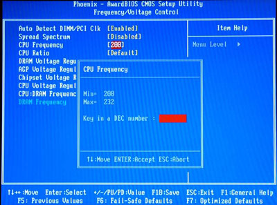
CPU only extends to 232FSB. This is probably adequate for a board without AGP/PCI lock, but we would have been happier to see a range to 250. Since SiS has implemented a “Fixed PCI/AGP” setting on other chipsets, we hope it is also possible on the 748 with a BIOS update.
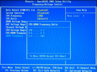
SiS is famous for the incredible array of memory options they have provided in chipsets like the 645/655 series, so we hoped we would be seeing a full range of memory ratios. The only choices are SPD, 1:1 (DDR400), and 6:5 (DDR333). We hope to see more choices in the shipping BIOS.
System and Memory Timings are adjusted in the Advanced Chipset Features menu.
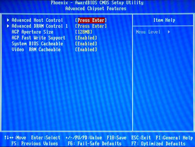
Memory adjustments are in submenu, called “Advanced Dram Control 1”. The Evaluation ROM has a very limited selection of settings. The only adjustments are “Normal” and “Performance”, and CAS values can only be selected if Performance is enabled. We suspect there will be additional memory timings available on the release DFI 748-AL.
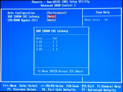
CAS 2 would not work with our Corsair 3200LL, which is SPD-timed at 2-2-3-6. Normal appears to set timings of 2.5-4-4-8 at SPD with the Corsair. Performance and CAS 2.5 set 2.5-4-4-5. Even with these very conservative timings, the DFI performed extremely well, but if the release BIOS improves the memory timings, we sill see a whole new level of performance.
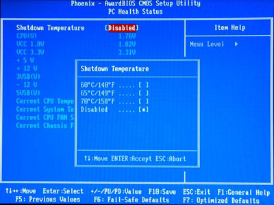
PC Health functions are included for monitoring functions, such as System and CPU temperatures, fan speed monitoring for 2 on-board fan connections, vCore, and Power Supply readings for all rails. DFI also offers options for setting shut-down temperatures for automatic system shut-down if a CPU overheats.
BIOS options for the 748-AL would be excellent on any board, but they are even more surprising on a SiS 748 board. We hope DFI will revamp the options for memory timings in the release BIOS, which are the only weak section of an otherwise strong BIOS. Options to 250FSB and PCI/AGP fix would also be welcome additions.
FSB Overclocking Results
In the past, when reviewing AMD motherboards, the only test method used at AnandTech was to remain at default multiplier while increasing the FSB until the highest stable FSB was reached. This method does report useful information for comparison, but there is another method for overclocking many recent Athlon motherboards. Most recent Athlon XP/Barton CPUs are unlocked or they behave as unlocked on recent motherboards. This allows overclocking by changing the multiplier or ratio of the Athlon CPU. On recent motherboards and Athlon CPUs, this requires no special “modification” to the board or CPU — it is now a standard feature available to any end-user who wants to use it. We have seen cases, like the DFI 748-AL that we are testing, where the FSB overclock is average or poor due to the lack of a PCI/AGP lock; when in fact, very high overclocks were possible by adjusting just the multiplier or both the multiplier and FSB.Since the multiplier or ratio adjustment is now a standard feature on many nForce2, KT600, and SiS 748 motherboards, we are adding a second overclocking test to Athlon reviews. We will also change multipliers and/or voltage on a reported air-cooling setup to find the highest stable overclock we can find using multiplier, voltage, and FSB with our standard components. We are not just looking for the highest number we could achieve. We will be trying to find a stable combination to provide an overclock that can still handle our stress testing. Both standard multiplier/highest FSB at default voltage and highest stable overclock will be reported.
The following setup was used on the DFI 748-AL for FSB overclocking:
| Front Side Bus Overclocking Testbed | ||||
| Default Voltage | Maximum Overclock | |||
| Processor: | Athlon XP 2500+ (Barton Core) |
Athlon XP 2500+ (1837MHz) (Barton Core – 11x166) |
||
| CPU Voltage: | 1.65V (default) | 1.775V | ||
| Cooling: | Thermalright SK-7 with 80mm Thermaltake Fan | Thermalright SK-7 with 80mm Thermaltake Fan | ||
| Power Supply: | Powmax 350W | Powmax 350W | ||
| Maximum OC: | 2332MHz (+27.3%) (11x212FSB) |
2450MHz (+33.4%) (12x204) |
||
Without a Fixed PCI/AGP bus speed, we expected the 748-AL would be limited in overclocking ability. The maximum stable overclock we could achieve at default voltage and multiplier was 212FSB. This is about the same as achieved on the better VIA KT600 boards, so we suspect that we may be seeing the AGP speed limit of the Radeon 9800 PRO video card more than the actual limit of the board. Fortunately, the DFI offers a full range of multipliers from 5X to 21X, and they work very well. We were able to set the FSB speed to a fixed 200 with the Dip switches on the board, increase the multiplier to 12.0 from 11.0 and mildly overclock the bus to 204 to achieve 2.45Gz with our Barton specified to run at 1.833GHz. This 33%+ overclock is close to the best we have achieved with this chip.
The nForce2 chipset, with PCI/AGP lock and a full range of multipliers, allows more possibilities with higher FSB options, but the DFI does allow the chip to reach its maximum speed with increased multipliers near one of the fixed FSB settings, like 200 and 166. What you can’t get without an AGP/PCI lock, are working settings like 10x240. The video card or PCI peripherals will likely give up before you can reach this setting.
The performance achieved from a board that will sell at a bargain price was excellent. The DFI is the only SiS 748 board with multiplier adjustments, and it does make a large difference in performance. We would be happier to see both a PCI/AGP frequency lock, and multipliers, but we were able to achieve excellent performance increases with the multiplier and FSB adjustments.
DFI 748-AL: Stress Testing
We performed stress tests on the DFI 748-AL in these areas and configurations:1. Chipset and motherboard stress testing, which was conducted by running the FSB at 212MHz; and
2. Memory stress testing, which was conducted by running RAM at 400MHz with 2 DIMM slots filled and at 400MHz with 3 DIMM slots filled at the lowest memory timings possible.
Front Side Bus Stress Test Results:
As standard practice, we ran a full range of stress tests and benchmarks to ensure the DFI 748-AL was absolutely stable at each overclocked FSB speed. These stress tests included Prime95 torture tests, which were run in the background for a total of 24 hours.In addition, we ran several other tasks — data compression, various DX8 and DX9 games, and apps, like Word and Excel — while Prime95 was running in the background. Finally, we ran our benchmark suite, which includes ZD Winstone suite, Unreal Tournament 2003, SPECViewperf 7.0, and Gun Metal Benchmark 2. While we were able to boot and run some tests at speeds as high as 217MHz FSB at default voltage on the 748-AL, 212MHz was the highest FSB overclock that we were able to achieve at default voltage with the Asus without encountering any reliability issues.
Memory Stress Test Results:
The memory stress test is very simple, as it tests the ability of the 748-AL to operate at its officially supported memory frequency (400MHz DDR) at the lowest supported memory timings that our Corsair TwinX LL modules support. The SPD timings for the Corsair v1.2 modules is 2-2-3-6, but without any real means to set individual memory timings on the 748-AL, we had to rely on other utilities to report real memory timings. CPUZ (www.cpuid.com) does not recognize the SiS 748 chipset memory controller, and we could not use it to determine memory timings. We had to depend on results reported in SiSoft Sandra Max3 Memory Test for memory timings. Sandra recognized the chipset correctly, but reported memory timings may not be 100% correct.| Stable Dual DDR400 Timings (2/3 banks populated) |
|
| Clock Speed: | 200MHz |
| Timing Mode: | Performance |
| CAS Latency: | 2.5 |
| Bank Interleave: | 4 |
| RAS to CAS Delay: | 4T |
| RAS Precharge: | 5T |
| Precharge Delay: | 4T |
| Command Rate: | N/A |
We did some experimenting with the “Normal” and “Performance” selections in BIOS. Normal memory timings are reported to be 2.5-4-4-8 in Sandra. When Performance is selected, CAS settings can be chosen, but CAS 2 would not work with the Corsair 3200LL modules or any other high-speed module that was tested. The lowest setting that works is “Performance”, “CAS 2.5” and Sandra timings are reported as 2.5-4-4-5.
Filling all 3 available memory banks is much more strenuous on the memory subsystem than testing 2 banks. With all 3 banks filled, the DFI 748-AL had no problems with the same timings that worked with 2 dimms.
| Stable DDR400 Timings (3/3 banks populated) |
|
| Clock Speed: | 200MHz |
| Timing Mode: | Performance |
| CAS Latency: | 2.5 |
| Bank Interleave: | 4 |
| RAS to CAS Delay: | 4T |
| RAS Precharge: | 5T |
| Precharge Delay: | 4T |
| Command Rate: | N/A |
We were pleased to see the DFI run with stability with 3 DDR400 dimms. With the limited Memory Timing options available, we really can't tell you much about memory timings with 2 and 3 dimms. Normally, 3 dimms requires timings a bit slower than 2, but until DFI adds memory timings in the release BIOS, we really can't tell you the fastest timings that will work on the 748-AL. It’s worth stating again that the real world performance difference between aggressive memory timings and more relaxed memory timings, such as SPD, are often very small. That is more than just words in this 748-AL review, as you will see in performance tests using these very slow memory timings.
We tested all these memory timings using several stress tests and general applications to guarantee stability. Prime95 torture tests were successfully run at the timings listed in the above charts. We also ran 3DMark and Super Pi. None of these stress tests created stability problems for the DFI 748-AL at these memory timings.
DFI 748-AL: Tech Support and RMA
For your reference, we will repost our support evaluation procedure here:
The way our Tech Support evaluation works is first, we anonymously email the manufacturer's tech support address(es), obviously not using our AnandTech mail server to avoid any sort of preferential treatment. Our emails (we can and will send more than one just to make sure we're not getting the staff on an "off" day) all contain fixable problems that we've had with our motherboard. We allow the manufacturer up to 72 (business) hours to respond, and then we will report whether or not they responded within the time allotted, and if they were successful in fixing our problems. In case we don’t receive a response before the review is published, any future responses will be added to the review, including the total time it took for the manufacturer to respond to our requests.
The idea here is to encourage manufacturers to improve their technical support as well as provide new criteria upon which to base your motherboard purchasing decisions. As motherboards become more similar everyday, we have to help separate the boys from the men in as many ways as possible. As usual, we're interested in your feedback on this and other parts of our reviews, so please do email us with your comments.
DFI’s easily obtainable RMA policy can be found by visiting their U.S. website at www.dfiusa.com and by clicking on the “Support” hyperlink at the menu listed on the left of their home page, which makes for simple, straightforward access. The international DFI site is linked from this site, or can be accessed at www.dfi.com. Further Technical Support and FAQ’s are available at this main site. If you would like to RMA your DFI motherboard, DFI suggests that you should first contact the vendor from where you purchased your motherboard before reaching out to DFI’s tech support and RMA.
For US customers, Technical Support is available by email at [email protected]. Since the DFI 748-AL is an Engineering Sample, we did not see any realistic way we could ask for technical support on an unreleased board and get response such that an average customer might receive. So, we did not go through our usual procedure of sending an email for tech support. Our past experiences with DFI technical support have been excellent, and we have seen nothing recently to change that opinion. We suspect you will continue to receive fast and helpful responses to your Tech Support questions for DFI products.
DFI offers very clear instructions for motherboard returns as well as any technical support questions — for both US and international customers. Those who cannot find a local resource should send their Tech Support inquiries to the main site in Taiwan. DFI seems to be expanding their on-line resources, and there was more on-line information available than we found in the last look at DFI. There is more good news, however, in that the information and resources are still easy to find – without going through endless links. DFI has done an outstanding job of making customer service a priority, and we think many of you will be pleasantly surprised at the responsiveness you will find in your contacts with DFI.
Performance Test Configuration
| Performance Test Configuration | |
| Processor(s): | AMD Athlon XP 3200+ (400MHz FSB) |
| RAM: | 2 x 256MB Corsair PC3200 TwinX LL (v1.1 or 1.2) Modules (SPD rated) |
| Hard Drive(s): | Maxtor 120GB 7200 RPM (8MB Buffer) Western Digital 120GB 7200 RPM Special Edition (8MB Buffer) |
| Video AGP & IDE Bus Master Drivers: | SiS AGP r1.16 & SiS IDE r2.04 NVIDIA nForce version 2.03 (1/30/03) VIA 4in1 Hyperion 4.47 (May 20, 2003) |
| Video Card(s): | ATI Radeon 9800 PRO 128MB (AGP 8X) |
| Video Drivers: | ATI Catalyst 3.6 |
| Operating System(s): | Windows XP Professional SP1 |
| Motherboards: | DFI 748-AL (SiS748)@200.45MHz FSB Asus A7V600 (KT600)@200.0 MHz FSB Soltek NV400-L64 (nForce2 400 SC)@ 200.5MHz FSB DFI NFII Ultra LANParty (nForce2 Ultra 400) @ 201.35 MHz FSB Gigabyte 7VT600 1394 (KT600) @ 202.78MHz FSB Gigabyte 7NNXP (nForce2 Ultra 400) @ 202.77MHz FSB Epox 8KRA2+ (KT600)@202.44MHz FSB |
All performance tests run on nForce2 400 (SC)/nForce2 Ultra 400 (DC) motherboards utilized two 256MB Corsair TwinX LL PC3200 (v1.1 or 1.2) modules set to SPD timings in DDR400 mode. Dual-Channel mode was used on nForce2 Ultra 400 boards, and 2 dimms working as Single-Channel were used on the nForce2 400 Soltek NV400-L64 board.
All performance tests that ran on the KT600-based motherboards used two 256MB Corsair TwinX LL PC3200 (v1.1 or 1.2) Corsair modules in DDR400 mode. KT600 memory timings did vary slightly among the motherboards, with the Asus A7V600 requiring a Ras-to-Cas of 3 for stable operation and other KT600 boards requiring a Ras-to-Cas setting of 2. 4-bank interleave and the highest available timing option (Turbo or Ultra) was used.
Performance tests were run with the ATI 9800 PRO 128MB video card with AGP Aperture set to 128MB with Fast Write enabled. The ATI 9800 PRO is the new AnandTech video card standard for reviews.
Additions to Performance Tests
Benchmark testing is dynamic, and we have added several new benchmarks to our standard Test Suite.1) ZD Labs Internet Content Creation Winstone 2003 — This benchmark has just been updated by ZD Labs and includes many new features in the Benchmark Suite, such as Media Encoding. It also uses the most up-to-date versions of Multimedia Creation software, which is rapidly changing as new software tools are released.
2) ZD Labs Business Winstone 2002 — ZD Labs Business Winstone has been around for many years and is a widely quoted Benchmark for measuring system performance. It basically provides a similar benchmarking suite to Sysmark 2002 Office Productivity.
3) Gun Metal DirectX Benchmark 2 — This demo/benchmark from Yeti Labs is one of the first DX9 game-based benchmarks available. Unlike some older benchmarks, such as Quake 3 that generate insane FPS ratings in the 300’s, we see performance numbers in the 30 to 40FPS range with current DX9 cards.
To give AnandTech readers a feel for how some of the newer benchmarks compare to the more familiar benchmarks used in past reviews, we have posted results for both the new benchmarks and Sysmark 2002, and all the games that have been a part of our standard benchmark suite.
New Hardware
With the release of DirectX 9 late in 2002, the availability of Benchmarks to test DX9, and the availability of DX9-supporting video cards from both nVidia and ATI, we are now using the ATI Radeon 9800 PRO for all hardware reviews.Content Creation and General Usage Performance
Media Encoding and Gaming Performance
High End Workstation Performance - SPEC Viewperf 7.0
High End Workstation Performance - SPEC Viewperf 7.0 (continued)
Final Words
The DFI 748-AL is a motherboard that shows the promise of the SiS 748 chipset. It has a full selection of tweaking and overclocking options that allow the end user to get the most from the 748 chipset. This includes a full working range of multiplier ratios, which have been absent from other SiS 748 designs. The tested board was an engineering sample with an evaluation ROM, but was still remarkably stable in everything we tested. The only glaring weakness was the lack of available memory timing options, which we expect will be fixed in the release BIOS.Even hampered by the current 2.5-4-4-8 timings at DDR400, the 748-AL still performs in the range of VIA KT600 boards. With better memory timings and setting options, it could easily out-perform the KT600 boards we have tested. However, unless there are some major miracles performed in the release BIOS, the DFI 748-AL is not likely to meet or pass the performance of the nForce2 Ultra 400 Athlon motherboards. We did not test hard-disk I/O, but SiS has performed very well in that area with recent chipsets. We suspect that benchmarks which heavily weight disk I/O, like Futuremark’s PCMark2002, will show much closer performance of the nForce2 Ultra 400 and the SiS 748 chipsets than we have found in our testing.
It is likely that DFI will have effective memory control options in the release BIOS, which will definitely improve performance. We also hope there is a way to add a “Fixed PCI/AGP” option to the final BIOS. It is available in other SiS chipsets, so we suspect it may be an option that DFI can incorporate in the final 748 BIOS. For the wish list, an increase of available FSB options from 232 to 250 would also be useful.
We commend DFI for their efforts to bring a full-featured SiS 748 design to market. With the market rolling with the nForce2 snowball, it must be a difficult decision whether to introduce a board like the 748-AL. There is much to like in the SiS 748, and it is certainly a worthwhile product. In the end, we don’t know if that will make much difference, since it does not win the performance crown from nForce2. At it's selling price, the DFI 748-AL is an excellent choice with many unique features provided by the SiS 748 chipset.


