Original Link: https://www.anandtech.com/show/11170/the-amd-zen-and-ryzen-7-review-a-deep-dive-on-1800x-1700x-and-1700
The AMD Zen and Ryzen 7 Review: A Deep Dive on 1800X, 1700X and 1700
by Ian Cutress on March 2, 2017 9:00 AM EST
For over two years the collective AMD vs Intel personal computer battle has been sitting on the edge of its seat. Back in 2014 when AMD first announced it was pursuing an all-new microarchitecture, old hands recalled the days when the battle between AMD and Intel was fun to be a part of, and users were happy that the competition led to innovation: not soon after, the Core microarchitecture became the dominant force in modern personal computing today. Through the various press release cycles from AMD stemming from that original Zen announcement, the industry is in a whipped frenzy waiting to see if AMD, through rehiring guru Jim Keller and laying the foundations of a wide and deep processor team for the next decade, can hold the incumbent to account. With AMD’s first use of a 14nm FinFET node on CPUs, today is the day Zen hits the shelves and benchmark results can be published: Game On!
[A side note for anyone reading this on March 2nd. Most of the review is done, bar an edit pass or two. Most of the results pages have graphs, but no text. Please have patience while we finish.]
Launching a CPU is like an Onion: There are Layers
As AnandTech moves into its 20th anniversary, it seems poignant to note that one of our first big review pieces that gained notoriety, back in 1997, was on a new AMD processor launch. Our style and testing regime since then has expanded and diversified through performance, gaming, microarchitecture, design, feature-set and debugging marketing strategy. (Fair play to Anand, he was only 14 years old back then…!). Our review for Ryzen aims to encompass many of the areas we feel pertinent to the scale of today’s launch.
An Interview with Dr Lisa Su, CEO of AMD
The Product Launch: A Small Stack of CPUs
Microarchitecture: Front-End, Back-End, micro-op cache, GloFo 14nm LP
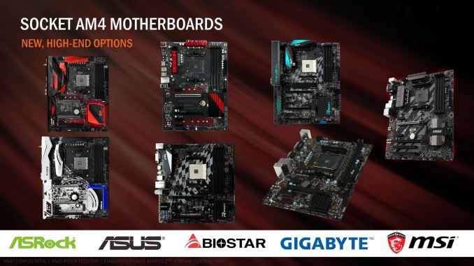
Chipsets and Motherboards: AM4 and 300-series
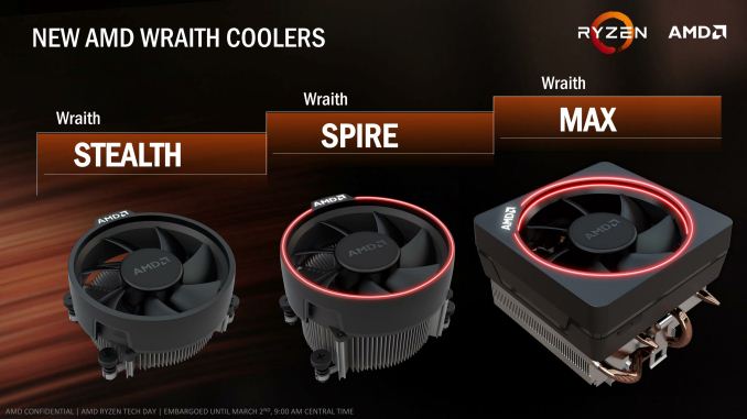
Stock Coolers and Memory: Wraith and DDR4
Benchmarking Performance: Our New 2017 CPU Benchmark Suite
Conclusions
Before the official launch, AMD held a traditional ‘Tech Day’ for key press and analysts in the past week over in San Francisco. The goal of the Tech Day was to explain Zen to the press, before the press explain it to everyone else. AMD likes doing Tech Days, with recent events in memory covering Polaris and Carrizo, and I don’t blame them: alongside the usual slide presentations recapping what is already known or ISSCC/Hot Chips papers, we also get a chance to sit down with the VPs and C-Level executives as well as the key senior engineers involved in the products. Some of the information in this piece we would have published before: AMD’s machine of tickle-out information means that we know a good deal behind the design already, but the Tech Day helps us ask those final questions, along with the official launch details.
So, What Is Zen? Or Ryzen?
A Brief Backstory and Context
The world of main system processors, or CPUs in this case, is governed at a high level by architecture (x86, ARM), microarchitecture (how the silicon is laid out), and process node (such as 28HPM and 16FF+ from TSMC, or 14LP from GloFo). Beyond these we have issues of die area, power consumption, transistor leakage, cost, compatibility, dark silicon, frequency, supported features and time to market.
Over the past decade, both AMD and their main competitor Intel have been competing for the desktop and server computer markets with processors based on the x86 CPU architecture. Intel moved to its leading Core microarchitecture on 32nm around 2010, and is now currently in its seventh generation of it at 14nm, with each generation implementing various front-end/back-end changes and design adjustments to caches and/or modularity (it’s actually a lot more complex than this). By comparison, AMD is running its fourth/fifth generation of Bulldozer microarchitecture, split between its high-end CPUs (running an older 2nd Generation on 32nm), its mainstream graphics focused APUs (running 4th/5th Generation on 28nm), and laptop-based APUs (on 5th Generation).
| High-Performance and Mainstream x86 Microarchitectures |
||||
| AMD | Year | Intel | ||
| Zen | 14FF | 2017 | ? | |
| Excavator v2 | GF28A | 2016 | 14+FF | Kaby Lake |
| Excavator | GF28A | 2015 | 14FF | Skylake |
| Steamroller | 28SHP | 2014 | 14FF | Broadwell |
| - | - | 2013 | 22FF | Haswell |
| Piledriver | 32 SOI | 2012 | 22FF | Ivy Bridge |
| Bulldozer | 32nm | 2011 | 32nm | Sandy Bridge |
| - | - | 2010 | 32nm | Westmere |
| K10 | 45nm | Other | 45nm | Nehalem |
AMD’s Bulldozer-based design was an ambitious goal: typically a processor core will have a single instruction entry point leading to a decode then dispatch to separate integer or floating point schedulers. Bulldozer doubled the integer scheduler and throughput capabilities, and allowed the module to accept two threads of instructions - this meant that integer heavy workloads could perform well, other bottlenecks notwithstanding. The perception was that most OS-based workloads are invariably integer/whole number based, such as loop iterations or true/false Boolean comparisons or predicates. Unfortunately the design ended up with a couple of key issues: OS-based workloads ended up getting more floating-point heavy, traditional OSes didn’t understand how to dispatch work given a dual-thread module leading to overloaded modules (this was fixed with an update), general throughput of a single thread was a small (if any) upgrade over the previous microarchitecture design, and power consumption was high. A number of leading analysts pointed to design philosophies in the Bulldozer design, such as a write-through L1 cache and a shared L2 cache within a module lead to higher latencies and increased power consumption. A good chunk of the deficit to the competition was the lack of a micro-op cache that can help bypass instruction decode power and latency, as well as a process node disadvantage and the incumbent’s strong memory pre-fetch/branch prediction capabilities.
The latest generation of Bulldozer, using ‘Excavator’ cores under the Carrizo name for the chip as a whole, is actually quite a large jump from the original Bulldozer design. We have had extensive reviews of Carrizo for laptops, as well as a review of the sole Carrizo-based desktop CPU, and the final variant performed much better for a Bulldozer design than expected. The fundamental base philosophy was unchanged, however the use of new GPUs, a new metal stack in the silicon design, new monitoring technology, new threading/dispatch algorithms and new internal analysis techniques led to a lower power, higher performance version. This was at the expense of super high-end performance above35W, and so the chip was engineered to focus at more mainstream prices, but many of the technologies helped pave the way for the new Zen floorplan.
Zen is AMD’s new microarchitecture based on x86. Building a new base microarchitecture is not easy – it typically means a large paradigm shift in the way of thinking between the old design and new design in key areas. In recent years, Intel alternates key microarchitecture changes between two separate CPU design teams in the US and Israel. For Zen, AMD made strides to build a team suitable to return to the high-end. Perhaps the most prominent key hire was CPU Architect and all-around praised design guru Jim Keller. Jim has a prominent history in chip design, starting with the likes of Freescale, to developing chips for AMD when they fighting tooth and nail with Intel in the early 2000s, then moving on to Apple to work on the A5/A6 designs. AMD were able to re-hire Jim and put a fire in his belly with the phrase: ‘Make a new high-performance x86 CPU’ (not in those exact simple words…. I hope).
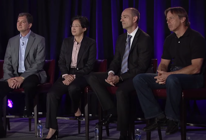
From left to right: Mark Papermaster (CTO AMD), Dr Lisa Su (CEO AMD),
Simon Segars (CEO ARM) and Jim Keller (former AMD, now Tesla)
Jim’s goal was to build the team and lay the groundwork for the new microarchitecture, which for the long-term will revolve around AMD Processor Architect Michael (Mike) Clark. Former Intel engineer Sam Naffziger, who was already working with AMD when the Zen team was put together, worked in tandem with the Carrizo and Zen teams on building internal metrics to assist with power as well. Mark Papermaster, CTO, has stated that over 300 dedicated engineers and two million man-hours have been put into Zen since its inception.
As mentioned, the goal was to lay down a framework. Jim Keller spent three years at AMD on Zen, before leaving to take a position under Elon Musk at Tesla. When we reported that Jim had left AMD, a number of people in the industry seemed confused: Zen wasn’t due for another year at best, so why had he left? The answers we had from AMD were simple – Jim and others had built the team, and laid the groundwork for Zen. With all the major building blocks in place, and simulations showing good results, all that was needed was fine tuning. Fine tuning is more complex than it sounds: getting caches to behave properly, moving data around the fabric at higher speeds, getting the desired memory and latency performance, getting power under control, working with Microsoft to ensure OS compatibility, and working with the semiconductor fabs (in this case, GlobalFoundries) to improve yields. None of this is typically influenced by the man at the top, so Jim’s job was done.
This means that in the past year or so, AMD has been working on that fine tuning. This is why we’ve slowly seen more and more information coming out of AMD regarding microarchitecture and new features as the fine-tuning slots into place. All this culminates in Ryzen, the official name for today’s launch.
Along with the new microarchitecture, Zen is the first CPU from AMD to be launched on GlobalFoundries’ 14nm process, which is semi-licenced from Samsung. At a base overview, the process should offer 30% better efficiency over the 28nm HKMG (high-k metal gate) process used at TSMC for previous products. One of the issues facing AMD these past few years has been Intel’s prowess in manufacturing, first at 22nm and then at 14nm - both using iterative FinFET generations. This gave an efficiency and die-size deficit to AMD through no real fault of their own: redesigning older Bulldozer-derived products for a smaller process is both difficult and gives a lot of waste, depending on how the microarchitecture as designed. Moving to GloFo’ 14nm on FinFET, along with a new microarchitecture designed for this specific node, is one stepping stone to playing the game of high-end CPU performance.
But returning to high-end CPU performance is difficult. There are two crude ways to measure performance: overall throughput, or per-core throughput. Having a low per-core throughput but using lots and lots of cores to increase overall throughput already has a prime example in graphics cards, which are mainly many small dedicated vector processors in a single chip. For general purpose computing, we see designs such as ThunderX putting 64+ ARM cores in a single chip, or Intel’s own Xeon Phi that has up to 72 x86 cores as a host processor (among others). All of these have relatively low general purpose single-core performance, either due to the fact that they focus on specific workloads, their architecture, or they have to run at super-low frequency to be within a particular power budget. They’re still high-performance, but the true crown lies with a good per-core performance. Per-core is where Intel has been winning, and the latest Skylake/Kaby Lake microarchitecture holds the lead due to the way the core is designed, tuned, and produced on arguably the most competitive manufacturing process node geared towards high performance and efficiency.
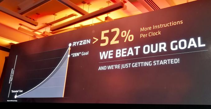
With the Zen microarchitecture, AMD’s goal was to return to high-end CPU performance, or specifically having a competitive per-core performance again. Trying to compete with high frequency while blowing the power budget, as seen with the FX-9000 series running at 220W, was not going to cut it. The base design had to be efficient, low latency, be able to operate at high frequency, and scale performance with frequency. Typically per-core performance is measured in terms of ‘IPC’, or instructions per clock: a processor that can perform more operations or instructions per Hz or MHz has a higher performance when all other factors are equal. In AMD’s initial announcements on Zen, the goal of a 40% gain in IPC was put into the ecosystem, with no increase in power. It is pertinent to say that there were doubts, and many enthusiasts/analysts were reluctant to claim that AMD had the resources or nous to both increase IPC by 40% and maintain power consumption. In normal circumstances, without a significant paradigm shift in the design philosophy, a 40% gain in efficiency can be a wild goose chase. Then it was realised that AMD were suggesting a +40% gain compared to the best version of Bulldozer, which raised even more question marks. At the formal launch last week, AMD stated that the end goal was achieved with +52% in industry standard benchmarks such as SPEC from Piledriver cores (with an L3 cache) or +64% from Excavator cores (no L3 cache).
Moving nearer to the launch, and with more details under our belts, it was clear that AMD were not joking but actually being realistic. Analyzing what we were told about the core design (we weren’t told everything to begin with) would seem to suggest that AMD, through this long-term CPU team and core design plan, have all the blocks in place necessary to do the deed. Aside from getting an actual chip on hand to test, analysts were still concerned about AMD’s ability to execute both on time and sufficiently to make a dent and recreate a highly competitive x86 market.
Throughout the lifetime of the Zen concept at AMD, they have seen a couple of corporate restructurings, changes at the high C-level executives, time when the company value dipped below the company asset value, restructuring of manufacturing and wafer deals with GlobalFoundries (which was spun out of AMD before Zen), sale and re-lease of major corporate buildings, and the integration/de-integration of the graphics team within the company. Within all that, Bulldozer didn’t make the impact it needed to, in part due to pre-launch hype and underwhelming results. Sales volumes have been declining (partly due to lower global PC demand), and server-based revenues have dropped to almost nil as we’ve not seen a new Opteron in five years. In short, revenue has been decreasing. AMD’s ability to get their finances under control, and then focus and execute, has been under question.
In the past few months, that outlook has changed. The top four executives involved in Zen, Dr. Lisa Su (CEO), Mark Papermaster (CTO), Jim Anderson (CVP Client) and Forrest Norrod (CVP Server), have been stable in the company for a few years, and all four have that air of quiet confidence. It is rather surprising to see three traditional processor engineers at the top of the chain for a CPU launch, rather than a sales or marketing focused executive – typically an engineer releasing a product with a grin on their face is often a good sign. Apart from that, AMD’s semi-custom revenues have increased through securing deals with the leading consoles, the GPU side of the company (Radeon Technology Group, headed under Raja Koduri) successfully executed at 14nm with mainstream parts in 2016, and for that confidence has AMD now trading at over $12/share, just under their 2004/2005 peak. At the minute a large number of individuals and companies are invested in AMD succeeding, both consumers and financials alike, and recent performance on execution has been a positive factor.
Since August, AMD has been previewing the Zen microarchitecture in actual pre-production silicon, running Windows and running benchmarks. With the 40%+ gain in IPC constantly being quoted, and now a +52% being presented, most users and interested parties want to know exactly where it sits compared to an equivalent Intel product. Back in August AMD performed a single, almost entirely dismissible, benchmark showing equivalent IPC of Zen with Broadwell-E (read our write up on that here, and reasons why it’s difficult to interpret a single benchmark). AMD had a ‘New Horizons’ (Ho-Ryzen, get it?) event in December and announcements at CES in January showing performance in gaming and encoding, in particular Handbrake. It is worth noting that Intel, as you would expect any competitor, went through each open source project AMD had used an implemented updates to assist dead/bad code (e.g. coalescing read/writes to comply with AMD/Intel design guidelines) or offer improvements (adding in 256-bit vector codes to combine consecutive 128-bit compute*), which is why some of the results from the launch today are different from what AMD has shown. (If anyone thinks this is ‘unfair’, it begs a bigger question as to how IPC is a good measure of performance if the code is IPC limiting itself, which is a topic for another day.) At the Tech Day, AMD went into further detail regarding various internal benchmarks, both CPU and gaming related, showing either near parity or a fair distribution of win/loss metrics, but ultimately giving better price/performance.
*In this instance, having 4 x 128-bit vector math usually creates 4 ops. Arranging code to 256-bit can give 2 x 256-bit for two ops, which takes two cycles on Zen per core but only one cycle on Intel’s latest.
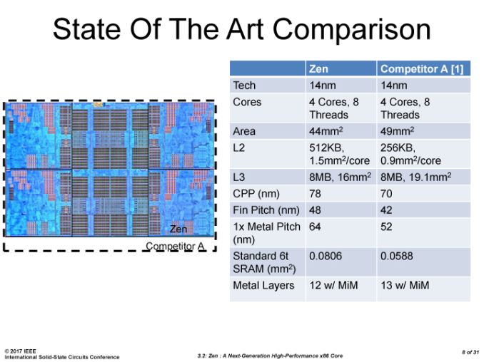
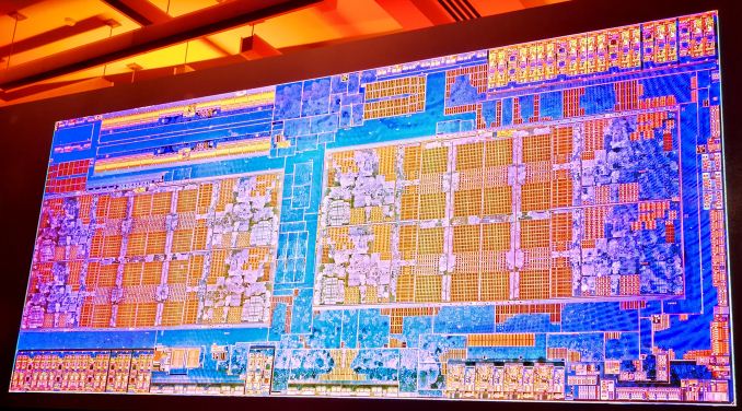
Recently AMD held a talk at ISSCC (the International Solid State Circuits Conference), which we’ll go into as part of this review, but one thing is worth mentioning here. Along with AMD requiring Zen to have good single thread performance, they also wanted something small. At ISSCC, AMD showed a slide comparing a Zen die shot to a ‘competitor’ (probably Skylake) die area:
Here AMD is comparing a four-core part to a four-core part, showing that while AMD’s L2 is bigger, the fin pitch is larger, the metal pitch is larger, and its SRAM cells are larger, the quad core design on 14nm GloFo is smaller than 14nm Intel. This is practically due to the way the Zen cores are designed vs. Intel cores – the simple explanation is that the Intel cores have wider execution ports (such as processing a 256-bit vector in one micro-op rather than two) and, we suspect, a larger area dedicated to pre-fetch logic. There’s also the consideration of dark silicon, to help assist the thermal environment around the logic units, which is undisclosed.
I mention this because one of AMD’s goals, aside from the main one of 40%+ IPC, is to have small cores. As a result, as we’ll see in this review, various trade-offs are made. Rather than dedicating a larger die area to execution ports that support AVX in one go, AMD decided to use 2x128-bit vector support (as 1x256) but increase the size of the L2 cache. A larger L2 will ensure fewer cache misses in varied code, perhaps at the expense of high-end compute which can take advantage of larger vectors. The larger L2 will help with single thread performance (all other factors being equal), and AMD knows that Intel’s cache is high performance, so we will see other trade-offs like this in the design. This is obviously combined with AMD’s recent work on having high-density libraries for cache and compute.
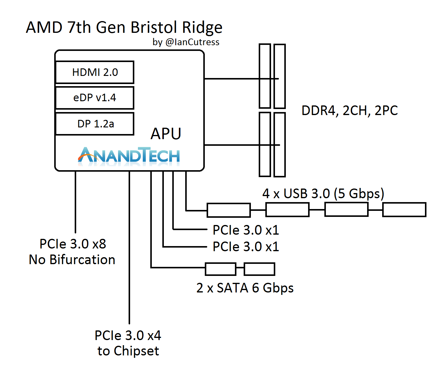
AMD has already set out a roadmap for different markets with products based on the Zen microarchitecture. Today’s launch is the first product line, namely desktop-class processors under the Ryzen 7 family name. Following Ryzen 7 will be Ryzen 5 (Q2) and Ryzen 3 (2H17) for the desktop. There is also AMD’s new server platform, Naples, featuring up to 32 cores on a single CPU (we’ll discuss Naples later in the review). We expect Naples to be in the Q2/Q3 timeframe. In the second half of this year (Q3/Q4), AMD is planning to launch mobile processors based on Zen, called Raven Ridge. This processor line-up will most likely be with integrated graphics, and it will be interesting to see how well the microarchitecture scales down into low power. As Ryzen CPUs are geared towards a more performance focused audience, and the fact that they lack integrated graphics, AMD will also maintain its line of ‘Bristol Ridge’ platform (Excavator based processors that also support the 300-series socket). The goal of Bristol Ridge is to fill in at the low end, or for systems that want the option of discrete graphics. Given what we’ve seen in benchmarks, despite recent statements from AMD to the contrary, the FX-line of AM3+ CPUs seems to be coming to an end.
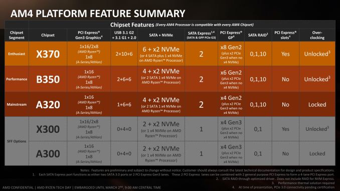
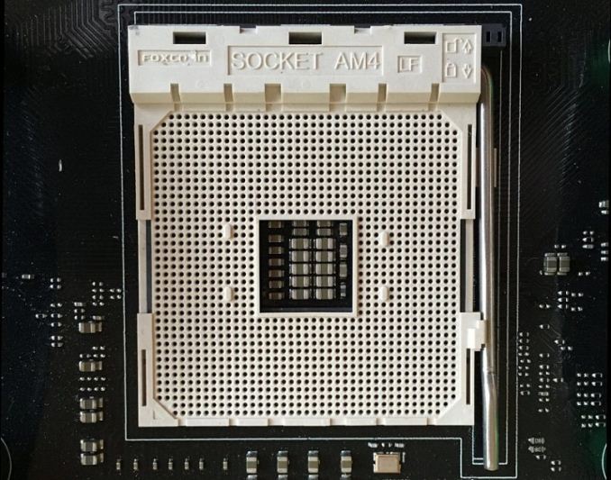
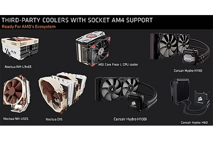
For users looking to go buy parts today, here’s the pertinent information you need to know. The Ryzen CPUs will form part of the ‘Summit Ridge’ platform – ‘Summit Ridge’ indicates a Ryzen CPU with a 300-series chipset (X370, B350, A320). Both Bristol Ridge and Summit Ridge, and thus Ryzen, mean that AMD makes the jump to a desktop platform that supports DDR4 and a high-end desktop platform that supports PCIe 3.0 natively. These CPUs use the AM4 socket on the 300-series motherboards, which is not compatible with any of AMD’s previous socket designs, and also has slightly different socket hole distances for CPU coolers that don’t use AMD’s latch mechanism. Despite the socket hole size change, AMD has kept the latch mechanism in the same place, but coolers that have their own backplates will need new supporting plates to be able to be used (we’ve got a bit on this later in the review as well).
An Interview with Dr. Lisa Su
AMD held a Tech Day a week before the launch of Zen to go over the details of of the new Ryzen product with the technology press. As part of these talks, we were able to secure Dr. Lisa Su, the CEO of AMD, for 30 minutes to discuss Zen, Ryzen, and AMD.
Profile:
Dr. Lisa Su, CEO of AMD. Born in Taiwan and educated at MIT, Dr. Su comes fully equipped with a Bachelors, Masters, and Ph.D. in Electrical Engineering. Before AMD, Dr. Su had appointments as CTO of Freescale Semiconductor, Director of Emerging Products at IBM, and a stint at Texas Instruments. It was at IBM that Dr. Su worked alongside Mark Papermaster, who is currently AMD’s CTO. Dr. Su was initially hired as SVP and GM at AMD, overseeing the global business units, and became CEO/COO in 2012. A rare occurrence, but Dr. Su is one of a small handful of female C-Level Executives in the semiconductor industry. Dr. Su has consistently been highly ranked in many 'top people to watch' lists of technology industry visionaries.
Ian Cutress: Congratulations on formally releasing Zen!
Q1: Both yourself and AMD officially have explicitly stated that AMD has needed to return back to the high-performance CPU market. We can all assume that there are still many hurdles ahead, but is getting Zen into retail silicon the spark that sets off the rest of the roadmap?
Lisa Su: I think launching Zen in desktop was a big big hurdle. That being said we have many others to go, and as you can imagine how happy I am. I know I’m only as good as my last product, so there’s a lot of focus on: Vega, Naples, Notebook, and 2018.
Q2: When we speak to some companies, they’ll describe that internally they have engineers working on the next generation of product, and fewer engineers working for the product after that, and continuing on for three, five or up to seven years of products. Internally, how far ahead in the roadmap do you have engineers working on product and product design?
LS: It’s at least 3 to 4 years. If you look at what we have on CPU and GPU, we have our roadmap out to 2020. It’s not set in stone, but we know the major markets and we adjust timings a quarter here or there as necessary.
Q3: A lot of analysts widely regard that rehiring Jim Keller was the right move for AMD, although at the time AMD was going through a series of ups and downs with products and financial issues. Was the 'new' CPU team shielded from those issues from day one, or at what point could the Zen team go full throttle?
LS: If I put credit where credit is due, Mark Papermaster had incredible vision of what he wanted to do with CPU/GPU roadmap. He hired Jim Keller and Raja Koduri, and he was very clear when he said he needed this much money to do things. We did cut a bunch of projects, but we invested in our future. Sure we cut things, but it was very clear. A note to what you said about Jim Keller though - he was definitely a brilliant CPU guy, but he was a part of that vision of what we wanted to do.
Q4: With Bulldozer, AMD had to work with Microsoft due to the way threads were dispatched to cores to ensure proper performance. Even though Zen doesn't have that issue, was there any significant back-and-forth with Microsoft to enable performance in Windows (e.g. XFR?)
LS: Zen is a pretty traditional x86 architecture as an overall machine, but there is optimization work to do. What makes this a bit different is that most of our optimization work is more on the developer side – we work with them to really understanding the bottlenecks in their code on our microarchitecture. I see many apps being tuned and getting better going on as we work forward on this.
Q5: How vital was it to support Simultaneous Multi Threading?
LS: I think it was very important. I think it was very complicated! Our goal was to have a very balanced architecture. We wanted high single threaded performance, and SMT was important given where the competition is. We didn’t want to apologize for anything with Zen – we wanted high single thread, we wanted many cores, but sorry we don’t have SMT? We didn’t want to say that, we wanted to be ambitious and give ourselves the time to get it done.
IC: Can you have your cake and eat it too?
LS: Yes! The key is to help the team to believe it can be done.
Q6: It has been noted that AMD has been working with ASMedia on the chipset side of the platform, using a 55nm PCIe 3.0x4 based chipset. Currently your competition implements a large HSIO model that can support up to 24 PCIe 3.0 lanes, albeit with limited bandwidth, but enables extensive networking, PCIe storage, and other features. What does AMD need to do to reach semi-parity for I/O ?
LS: I think we will continue to want a rich ecosystem. On the chipset side we may not develop the chipsets ourselves but we certainly want to be in partnership with others to develop a wide set of IO. I think if you look at the set of motherboard partners that we have, and the extensive testing we’ve done with them, I would expect that as we gain some market share in the high-end, you will see that system build up.
Q7: A couple of years ago, AMD's market value was lower than its assets. Today, it is trading over $10. A cynic would say that the increase has been a good Polaris launch combined with recent marketing cycles slowly giving out small bits of information. What's your response to AMD's recent share price rise over the past 12 months?
LS: My view is that I can never predict the market, so I never try! The market has a mind of its own. But what I can say is that we had some very key fundamentals. We are in key markets like the PC market, the cloud market, the infrastructure market, gaming – these are big big markets. They are growing too – I think that the markets we are in are good. We had to convince people fundamentally that we could execute a competitive roadmap and 18 months ago I’d say people didn’t really believe. They thought ‘ah well, maybe’, but ‘we don’t know’ is a power point. Over the past 6-9 months we’ve proven that we can gain graphics share, with the launch of Polaris, and with the launch of Ryzen I think you’ll see that we can convince that we can execute on high performance CPUs. Importantly our customers have become convinced too. The key thing with our customers is that when it was a power point, they weren’t sure: it was interesting, but it could have been six months late or have 20% less performance. When we actually gave them samples, they were actually like ‘Wow, this is actually real!’ and they started pulling in their schedules. So when you ask me about investors it’s something like that. I think people want some proof points to believe they can trust us and that if we execute that we’ll do ok.
Q8: Do you find that OEMs that haven’t worked with AMD are suddenly coming on board?
LS: I will say that we have engagements with every OEM now on the high-performance space. Twelve months ago, a number of them would have said that they don’t have the resources to do multiple platforms. So yes, I think momentum helps in this space.
Q9: At Intel's recent Investor Day we learned that future chips will incorporate multiple dies on the same package. This allows a semiconductor firm to focus on smaller chips and potentially better yields at the expense of some latency. Given what we predict will happen, what is your opinion on having large 600mm2 silicon? Is there a future?
LS: There has been a lot of debate on this topic. I find it a very interesting debate. Certainly on the graphics side we view High Bandwidth Memory (HBM) and the ability to get that interconnect between the GPU and memory to be extremely differentiating. So certainly we will use that throughout our graphics roadmap. If you look at our CPU roadmap, I do think there’s a case to be made for multi-chip modules. It depends on the trade-offs you have to do, the bandwidth requirements you have, but yes as the process technology becomes more complicated, breaking up the tasks does make sense.
Q10: With high-end GPUs, we commonly approach 250-300W power consumption. Why has the CPU stalled around 75-140W by comparison? Does AMD ever look to designing a CPU that actually aims for a power/efficiency sweet-spot north of 200W? Why hasn’t the high-performance CPU market gone and matched the GPU market in power consumption?
LS: That’s a good question, let me see if I’ve thought about that. I think we’re limited by other things on the CPU side. I think we’re limited by some reliability.
IC: But if you engineer for a specific power window…
LS: Sure but if you think about it, GPUs tend to be a lot more parallel, so that’s what drives the power. With CPUs, you might argue with me about whether you actually need eight cores, or not! I have to think about that answer, but I think that’s the right one – the difference between a very parallel machine and one that is less parallel.
Q11: Despite the differences, a lot of fingers point to the Zen microarchitecture floorplan and see significant similarities in the layout with Intel's Core microarchitecture. Without a fundamental paradigm shift, it seems we might be 'stuck' (for lack of a better term) with this kind of layout for perhaps a decade. How does AMD approach this, given your main competitor can easily invest in new seed firms or IP?
LS: The way I look at it, and I get asked this question very often (sometimes phrased a bit differently) – your competition can invest so much more than you can, how can we be competitive? I think the simple answer is in that yes we are smaller, but I think that we are also more focused. I think that sometimes with constraints comes creativity and so when you’re talking about what processors look like 5-10 years from now, if you look at the innovation in the last 10 years , a bunch of that has come from AMD. You tend to solve problems when you’re put in a box that you have to live in, so when we look at possible microarchitectures, there are still a lot of ideas out there. There’s still a lot of opportunity to incrementally improve performance. I think the difference is that you used to be able to say ‘let me just shrink it’ and it will go faster, and that is a process that lends itself to money as you can just buy equipment to shrink it. Today you have to handcraft it a bit more, and that lends itself to more creativity I would say.
Q12: We've recently seen your competitor announce a change in strategy regarding new process nodes, new architectures, and how markets will take advantage of the latest CPU designs. With Zen, AMD is first launching desktop, then server, then mobile: you've already mentioned Zen-plus on the roadmap - is the desktop-server-mobile roll-out method the best way for AMD to move forward?
LS: Not necessarily. I think for this generation [our strategy] made a lot of sense. I think the desktop and server use very similar kind of tuning, they’re both tuned for higher frequency and higher performance. The desktop is a bit simpler; the ecosystem for desktop is a bit simpler. The server has a more complicated testing setup that needs to run so that gives some context there. We really wanted to have a product in the high-end space. It was more set the market strategy than a technical strategy.
Q13: AMD currently has a very active semi-custom business, particularly when it comes to silicon design partnerships and when it comes to millions of Consoles. Speaking of custom silicon in consoles, current generation platforms currently use AMD’s low power ‘cat’ cores. Now that AMD has a small x86 core in Zen, and I know you won’t tell me what exactly is coming in the future, but obviously future consoles will exist, so can we potentially see Zen in consoles?
LS: I think you know our console are always very secretive about what they are trying to do, but hypothetically yes I would expect Zen to show up in semi-custom opportunities including perhaps consoles at a certain point in time.
Q14: AMD is in a unique position for an x86 vendor, with significant GPU IP at its beck and call. Despite the recent redefinition of the GPU group under RTG, would/has AMD ever consider using joint branding (similar to how ASUS markets ROG motherboards and GPUs for example)?
LS: What I’d like to say is (and you’ll appreciate this) that I love CPUs and GPUs equally, and the markets are a little bit different. And so think about it this way: our GPUs have to work with Intel CPUs, and our CPUs have to work with NVIDIA GPUs, so we have to maintain that level of compatibility and clarity. That being said, I think with Ryzen you can imagine that as we launch Vega later in the year that you might here about Ryzen plus Vega in systems because they are both high-performance things and we want to build great systems! I don’t know about co-marketing, but the idea of being able to say that ‘A plus A builds a great system’ is something we will do.
On the vendors who do motherboards and GPUs, I agree it takes a lot of work to bring out a new brand. We do view though that the way that people who buy CPUs and the people who buy GPUs do overlap, but they are still quite distinct.
Q15: Ryzen is priced very competitively compared to the competition, and it follows the common thinking that AMD is still the option for a cheaper build. Is that a characteristic that sits well with AMD?
LS: I think you should judge that question by what the 200 system integrators will be building with Ryzen in, and what the OEMs will be building. My view is that they system needs to be good enough for the CPU being putting in it. We are very picky about it, and we want Ryzen to be in high-end systems. Will we see Ryzen in some mainstream systems then sure, but if you look at our introduction order, there’s a reason why we’re going Ryzen 7 first, because it sets the brand. You know I want to sell millions and millions of processors, and I’ll sell a bunch that is less than eight cores but having that eight cores and sixteen threads defines what we’re capable of.
Q16: We've all seen the details of how desktop PC sales are down, but PC gaming revenue is increasing. There is no doubt that Ryzen will be marketed as a chip for gamers; how do you see consumers reacting to Ryzen?
LS: I think PC gaming is doing quite well, which is one of the hot markets. We are addressing as a gamers as a very important segment, but they are one of many important segments of users for us. We think Ryzen is a great gaming CPU, and you’ll test that for yourself – we’re not going to win every head-to-head, but if you think about gaming do you want theoretical performance or do you want the CPU to be good enough to showcase your GPU? I think what Ryzen allows is those folks to do something more than just gaming. So your gaming CPU might only uses four cores, but if you are doing video editing or streaming it will do a lot more. So I think what we’re trying to address is maybe the forward thinking users, not just the today gamer.
Q17: A perennial question we get asked is 'Core i7, i5 or i3?'. There have been countless reviews and YouTube videos on the subject. With Ryzen in the mix, what becomes the new question?
LS: I think you should help your users through that! I really think that’s the case. Ryzen 7 offers phenomenal capability for an eight-core, sixteen-thread device. As we introduce the next families you will see positioning but the end result is that you will see a top to bottom stack with a processor for everyone. At every price we will offer more performance. You will be able to see that in your own testing.
Q18: Can you comment on whether Bristol Ridge will be available to consumers at any point?
LS: Yes, good question. The answer is yes. The idea is that if you have an AM4 platform you can put an APU in there. As you saw we put Ryzen 7 first I think the intent was to ensure that AM4 was solidified on Ryzen. I say yes because that has always been the strategy for the AM4 socket to have a very long life and a very broad range. Exact timing has not yet been finalized.
Q19: At the high-end, Ryzen 7 is competing with Intel's high-end desktop market. But where Intel has 28/40 native PCIe 3.0 lanes, Ryzen only has sixteen. Avago PLX switches are almost $100 each, which means a route to 2 full-bandwidth GPUs or >3 GPUs or more NVMe is hindered. Was sixteen PCIe 3.0 the right choice?
LS: We think so, I mean we do. If you look at the distribution of PCs going into workstation I think that’s where the volume is. We still believe in the relative balance of performance and power in our decision, but it’s an interesting point.
Q20: Your competition has had success with both 'Core' parts and 'Xeon' parts, with the latter being ECC and vPro and having the professional feature-set. With the launch, AMD does have its 'Pro' CPU line, but this is more for business agreements and not yet dealing with Ryzen. Does AMD discuss this internally?
LS: I think what you should expect that Naples will go head to head in the server space, including single socket and dual socket. What you might be asking is if we are going to do something in between on the workstation stuff – I think it is fair to say that we view it all as interesting markets. To your question of ‘do we think about it?’, sure. With everything you roll out with a set of priorities so we set on consumer first, then we are going to do data center, and then we will see what will come next.
Q21: Is there room for an 'Opteron' as a brand name?
LS: You tell me!
IC: I think so! I spoke to a few people today and reactions were mixed. Obviously coming up with a new brand name for a product line is difficult. I assume there is conversation internally, as I don’t suspect the product to be called Naples at launch.
LS: I think you have hit on a topic that has had a good amount of debate [internally]. As we get closer to launch we will talk about branding on the server. But yes, it will not be called Naples in the market.
Q22: AMD is formally launching Ryzen with AMD benchmark data and pre-orders on 2/22, but no third-party data until the official launch of 3/2. A lot of customers see value on third-party independent verified data, and might perhaps see this tactic in a bad light. Can you comment on the reasons for the launch structure?
LS: We had a couple of things going on internally, to give you all our thought process. Because we were going so wide on the ecosystem in terms of sampling – motherboard sampling, system integrators, a lot of OEMs, and lot of ODMs, there has been (at least to my expectation) more chatter in the marketplace than I would have thought just in terms of things that are out there. Some of them were true, some were not true…
IC: Fake News!
LS: Ha! Our view was that we wanted to go through the review process very very diligently, and we also wanted to own the news as the news cycle was coming out. So the whole idea of taking the press out on the town to some boat or something, we thought that these guys are writing is real, so give them time to perhaps not do a full review but at least get comfortable with what you are seeing. I’ve said it before and I’ll say it again: everything we show you, what you see is what you get.
IC: The problem is the perception that perhaps that up to that point, every personal in the chain that has ‘data’ wants to sell you something.
LS: My view is that you guys are very smart guys, and you said you can do a lot in six hours!
(I had mentioned previously I had bought 10kg of testing kit to Tech Day to test Ryzen in my hotel room that evening before catching a flight out.)
AMD Ryzen 7 Launch Details
The Ryzen family of CPUs is designed to compete, initially, in the performance-mainstream and high-end desktop market. At first will be the launch of Ryzen 7 CPUs, a trio of eight-core, sixteen-thread designs, with Ryzen 5 and Ryzen 3 coming in Q2 and 2H17 respectively. Out of the CPUs we know about, the Ryzen 7 parts, the processors have a TDP of either 65W or 95W, and prices will range from $330 to $500.
| AMD Ryzen 7 SKUs | ||||||
| Cores/ Threads |
Base/ Turbo |
L3 | TDP | Cost | Launch Date | |
| Ryzen 7 1800X | 8/16 | 3.6/4.0 | 16 MB | 95 W | $499 | 3/2/2017 |
| Ryzen 7 1700X | 8/16 | 3.4/3.8 | 16 MB | 95 W | $399 | 3/2/2017 |
| Ryzen 7 1700 | 8/16 | 3.0/3.7 | 16 MB | 65 W | $329 | 3/2/2017 |
All the processors will be using the AM4 socket, with bases frequencies from 3.2 GHz to 3.6 GHz, and turbo frequencies up to 4.0 GHz for the high-end parts. The base design supports 512KB of private L2 cache per core and 2MB of a shared exclusive L3 victim cache.
The CPUs follow a naming scheme which most CPU enthusiasts will be familiar with:
- The high-end parts are ‘Ryzen 7’, which all happen to be eight-core parts and start around $300-$320. With a fully enabled chip, 16MB of L3 cache is available.
- In the mid-range are ‘Ryzen 5’ processors, set to be launched in Q2, which are all eight-core parts under the hood but are either 6-core parts or 4-core parts depending on the model. Leaks would tend to suggest that despite having two cores disabled, the 6-core parts still have access to all the L3 cache.
- At the bottom are ‘Ryzen 3’, due 2H17, all of which are quad core parts but do not have hyperthreading.
- All parts support overclocking.
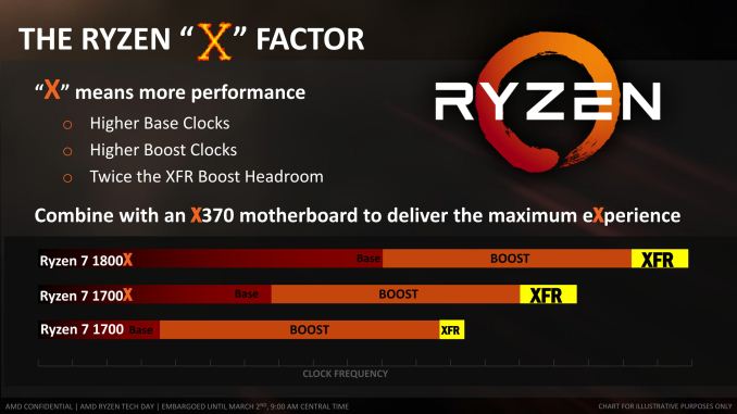
- Technically all parts support XFR, although only X can overclock with XFR (more on this later)
- It’s worth noting that ‘Ryzen 7 1900X’ is a gap waiting to be filled.
The formal name for these CPUs is ‘Ryzen 7’ followed by the SKU number. Having conversations with AMD, and noting that I suspect these names will colloquially be shortened to R7, R5 and R3 very quickly, we will be following convention and using the formal CPU names.
All these parts come from a single silicon design, with binning to ensure that the quality of each silicon die gets placed in the right bin. It is worth noting AMD’s tactics to launch a handful of SKUs at once follows on from its previous strategy. Part of it is a function of size (AMD by contrast to other players is actually small), and it allows AMD to react to how the market changes, as well as adjust product lines due to factors in the production (such as better semi-con characteristics).
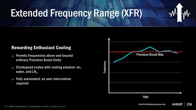
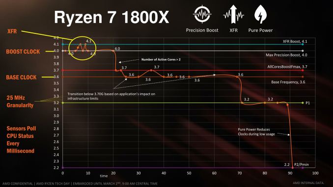
All the CPUs are multiplier unlocked, allowing users to go overclocking when paired with the X370 or B350 chipset. At this point we’re unsure what the upper limit is for the multiplier. We have been told that all CPUs will also support XFR, whereby the CPU automatically adjusts the frequency rather than the OS based on P-states, but the CPUs with ‘X’ in the name allow the CPU to essentially overclock over the turbo frequency. XFR stands for ‘eXtended Frequency Range’, and indicates that the CPU will automatically overclock itself if it has sufficient thermal and power headroom. We’ll mention it later, but XFR works in jumps of 25 MHz by adjusting the multiplier, which also means that the multiplier is adjustable in 0.25x jumps (as they have 100 MHz base frequency). XFR does have an upper limit, which is processor dependent. All CPUs will support 25 MHz jumps though XFR above the P0 state, but only X CPUs will go beyond the turbo frequency.
A side note: As to be expected, XFR only works correctly if the correct setting in the BIOS is enabled. At this point the option seems to be hidden, but if exposed it means it is up to the motherboard manufacturers to enable it by default – so despite it being an AMD feature, it could end up at the whim of the motherboard manufacturers. I suspect we will see some boards with XFR enabled automatically, and some without. We had the same issue on X99 with Turbo Boost 3, and Multi-Core Turbo.
So Why No Ryzen 5 or Ryzen 3?
AMD is remaining relatively quiet on the other Ryzen CPUs. At the Tech Day, we were told about one other CPU: the Ryzen 5 1600X.
| AMD Ryzen SKUs | ||||||
| Cores/ Threads |
Base/ Turbo |
L3 | TDP | Cost | Launch Date | |
| Ryzen 7 1800X | 8/16 | 3.6/4.0 | 16 MB | 95 W | $499 | 3/2/2017 |
| Ryzen 7 1700X | 8/16 | 3.4/3.8 | 16 MB | 95 W | $399 | 3/2/2017 |
| Ryzen 7 1700 | 8/16 | 3.0/3.7 | 16 MB | 65 W | $329 | 3/2/2017 |
| Ryzen 5 1600X | 6/12? | 3.6/4.0 | 16 MB? | ? W | N/A | Q2 2017 |
| Ryzen 3 ? | 4/4? | ? | 8 MB? | ? W | N/A | H2 2017 |
This six-core part will have two CPU cores disabled, though it is unclear if AMD will disable one core per cluster of four (giving a 3+3 arrangement) or if they could disable two from one cluster (giving 2+4). Nonetheless, it maintains the 3.6 GHz base frequency and 4.0 GHz turbo frequency similar to the Ryzen 7 1800X. This puts it square in the firing line of the Core i7-6850K (six core, Broadwell-E) and Core i7-5930K (six core, Haswell-E).
Ryzen 5 is scheduled for ‘Q2’, meaning the second quarter of 2017, or April-to-June inclusive. The big event in that time frame in the PC world is Computex at the beginning of June, which might be an apt time to launch some other products as well. The scale of the Ryzen 5 launch is unknown, and I suspect that if the demand for Ryzen 7 is high then AMD might not have enough CPUs to go around. If enough parts come out of the Fab working well, and Ryzen 7 is still selling strong, then we might have to wait for Ryzen 5. This aids part of AMD’s trickle-out strategy, though based on some of the comments we’re seeing online, Ryzen 5 is also highly anticipated.
The Ryzen 3 family is even more unknown. At this point the leaks suggest that these will be quad core parts without simultaneous multi-threading, however AMD has not released any information as to how they will work. The only thing we know is that AMD is planning a H2'17 launch, meaning the second half of 2017. That’s a very, very wide window, encompassing things like the Server chips launch but also the notebook SoCs. I suspect AMD will be constantly looking at their product lines and sales, determining what opportunities there are for Ryzen 3 CPUs – if they get a full launch or end up a footnote if the rest of the stack performs above expectations. Or Ryzen 3 could end up mobile only, but that’s just a low-chance hypothesis.
I saw Ryzen Pro being in the leaks?
At this time AMD is not announcing any Pro parts, although it was confirmed to be that there are plans to continue the Pro line of CPUs with Ryzen to be launched at a later time. These parts will be similar in practice to previous ‘Pro’ models we saw with Kaveri and Carrizo: designed for the big OEMs as an indication of large-contract support. AMD’s prominent partners for this are HP, Lenovo and Dell. These processors will most likely not be sold to the public, although OEM resellers typically get hold of a few. That means availability at this point is unknown. AMD states that multiplier overclocking is supported on all processors, however at the time of writing we’re unsure if that would naturally include the ‘Pro’ line. My gut instinct says ‘probably’, although the systems these CPUs will go into will likely have overclocking disabled, so it would have to be placed into a consumer motherboard.
A side note on ECC: given the design of Naples and the fact that it should be supporting ECC, this means that the base memory controller in the silicon should be able to support ECC. We know that it is disabled for the consumer parts, but nothing has been said regarding the Pro parts. We can confirm that ECC is enabled on the consumer Ryzen parts.
The Competition
Just after Tech Day, I ran a twitter poll regarding comparisons that my followers were interested in. The poll results were as follows:
So what CPU comparison is more vital for you? (for other suggestions, simply reply)
— Ian Cutress (@IanCutress) February 24, 2017
That’s
- 32% for the Ryzen 7 1800X vs Core i7-7700K,
- 31% for the Ryzen 7 1700 vs Core i7-7700K
- 25% for the Ryzen 7 1800X vs Core i7-6900K
- 11% for the Ryzen 7 1700 vs Core i7-2600K
- Mentions for
- Core i3-7350K numbers,
- Core i5-7600K numbers,
- Ryzen 5 1600X numbers (no can do before R5 launch)
- 1800X vs i7-5960X,
- 1700X vs 7700K,
- 1700X vs 6900K,
- DRAM testing,
- single thread testing,
- Maximum OC on each Ryzen part
- SPEC06 vs A10
- Dual Core Ryzen at 800 MHz vs Core m3 to simulate passive tablets
Naturally AMD has suggested processors which it feels offer direct competition against the various Ryzen CPUs. These are as follows:
| Comparison: Ryzen 7 1800X vs Core i7-6900K | ||
| AMD Ryzen 7 1800X |
Features | Intel Core i7-6900K |
| 8 / 16 | Cores/Threads | 8 / 16 |
| 3.6 / 4.0 GHz | Base/Turbo | 3.2 / 3.7GHz |
| 16 | PCIe 3.0 Lanes | 40 |
| 16 MB | L3 Cache | 20 MB |
| 95 W | TDP | 140 W |
| $499 | Price (MSRP) | $1049 |
At the top end we see the eight-core R7 1800X put directly against a Broadwell-E based eight-core Core i7-6900K. The Ryzen 7 1800X sits at 3.6 GHz base and 4.0 GHz turbo for 95W, while the Core i7-6900X is 3.2G/3.7G for 140W. The i7-6900K has the bigger L3 cache and more PCIe lanes, but costs twice as much ($1049 vs. $499).
| Comparison: Ryzen 7 1700 vs Core i7-7700K | ||
| AMD Ryzen 7 1700 |
Features | Intel Core i7-7700K |
| 8 / 16 | Cores/Threads | 4 / 8 |
| 3.0 / 3.7 GHz | Base/Turbo | 4.2 / 4.5 GHz |
| 16 | PCIe 3.0 Lanes | 16 |
| 16 MB | L3 Cache | 8MB |
| 65 W | TDP | 91 W |
| $329 | Price (MSRP) | $350 |
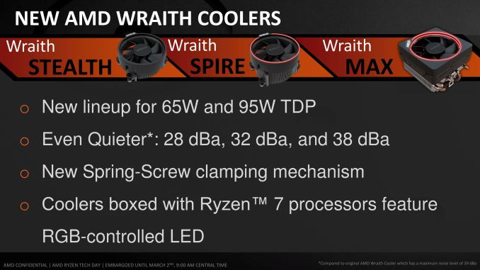
In the mid-range, the Ryzen 7 1700 is so near in price to the Core i7-7700K that it is hard to miss. The i7-7700K is based on Intel’s latest Kaby Lake microarchitecture, which AMD has already shown is ahead of the game compared to Zen. So while Intel gets a frequency advantage (4.2G/4.5G vs 3.0G/3.7G) and is likely to have a fundamental IPC advantage, the AMD Ryzen 7 1700 comes with eight cores over four, and has 16MB of L3 cache compared to 8MB on Intel. The 1700 and 7700K are similar in price ($330 vs $350) but the 1700 also comes with a new variant of AMD’s high performing Wraith cooler.
| Comparison: Ryzen 5 1600X vs Core i5-7600K | ||
| AMD Ryzen 5 1600X |
Features | Intel Core i5-7600K |
| 6 / 12 | Cores/Threads | 4 / 4 |
| 3.6 / 4.0 GHz | Base/Turbo | 3.8 / 4.2GHz |
| 16 | PCIe 3.0 Lanes | 16 |
| 16 MB? | L3 Cache | 6 MB |
| ? | TDP | 91W |
| ? | Price (MSRP) | $239 |
Because we know some specs already, it’s worth pointing out about the Ryzen 5 1600X. Expected pricing should put it close to the price of the Core i5-7600K, but offering three times as many threads. The Ryzen 5 will be down on frequency, but cache and cores is hard to miss. When we get in the Ryzen 5 samples it is sure to be a major test.
The validity of these comparisons will come down to how well AMD has executed in single core performance, and if having the L3 as an exclusive victim cache actually hampers performance, especially in memory heavy workloads such as compression.
Typically we would expect fewer cores at the same power to be clocked higher as there is TDP to spare. However, these four core designs can differ between two successive chips. The base design of all of these CPUs is a set of eight cores, split into two quad-core ‘Core Complexes’ (known as a CCX). Each CCX has four cores and 8MB of L3 cache, but are still part of the same silicon die and connected by the new Infinity Fabric. For a quad core design, four of those cores (and their L3 caches) are disabled, however it is never guaranteed which ones. Users could end up with 4+0, 1+3 or 2+2 cores active per CCX, which gives a slightly skewed latency response when having to pull memory from other caches. Because the L3 cache is an exclusive victim cache, this won’t happen as often as perhaps an inclusive cache might, but as a result it is expected that the reduce frequency might be to compensate for the different CCX configurations that might exist.
Zen: New Core Features
Since August, AMD has been slowly releasing microarchitecture details about Zen. Initially it started with a formal disclosure during Intel’s annual developer event, the followed a paper at HotChips, some more details at the ‘New Horizon’ event in December, and recently a talk at ISSCC. The Zen Tech Day just before launch gave a chance to get some of those questions answered.
First up, let’s dive right in to the high-level block diagram:
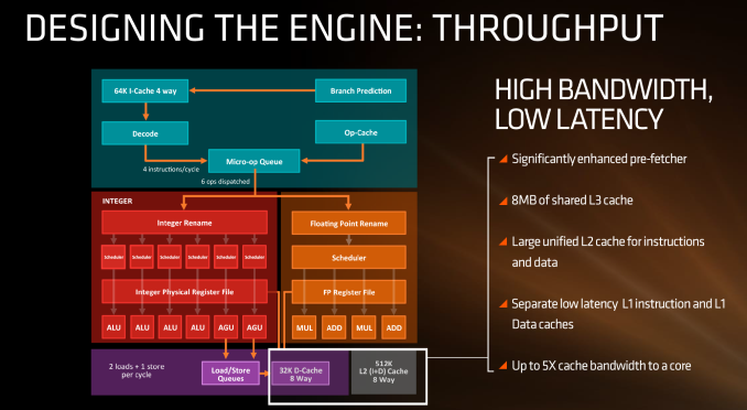
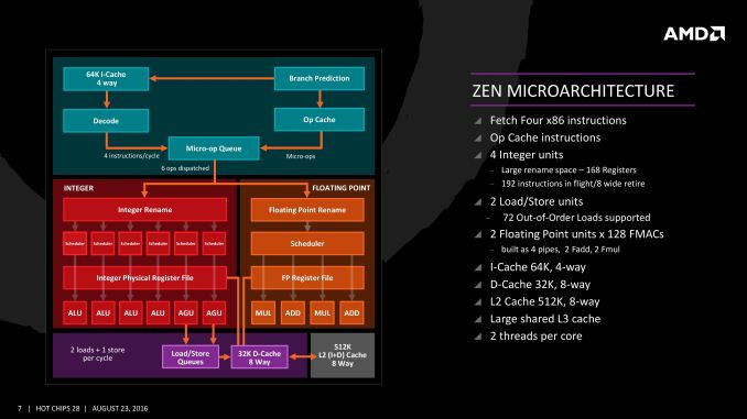
In this diagram, the core is split into the ‘front-end’ in blue and the rest of the core is the ‘back-end’. The front-end is where instructions come into the core, branch predictors are activated and instructions are decoded into micro-ops (micro-operations) before being placed into a micro-op queue. In red is the part of the back-end that deals with integer (INT) based instructions, such as integer math, loops, loads and stores. In orange is the floating-point (FP) part of the back-end, typically focused on different forms of math compute. Both the INT and FP segments have their own separate execution port schedulers
If it looks somewhat similar to other high-performance CPU cores, you’d be correct: there seems to be a high-level way of ‘doing things’ when it comes to x86, with three levels of cache, multi-level TLBs, instruction coalescing, a set of decoders that dispatch a combined 4-5+ micro-ops per cycle, a very large micro-op queue (150+), shared retire resources, AVX support, and simultaneous hyper-threading.
What’s New to AMD
First up, and the most important, was the inclusion of the micro-op cache. This allows for instructions that were recently used to be called up to the micro-op queue rather than being decoded again, and saves a trip through the core and caches. Typically micro-op caches are still relatively small: Intel’s version can support 1536 uOps with 8-way associativity. We learned (after much asking) at AMD’s Tech Day that the micro-op cache for Zen can support ‘2K’ (aka 2048) micro-ops with up to 8-ops per cache line. This is good for AMD, although I conversed with Mike Clark on this: if AMD had said ‘512’, on one hand I’d be asking why it is so small, and on the other wondering if they would have done something different to account for the performance adjustments. But ‘2K’ fits in with what we would expect.
Secondly is the cache structure. We were given details for the L1, L2 and L3 cache sizes, along with associativity, to compare it to former microarchitectures as well as Intel’s offering.
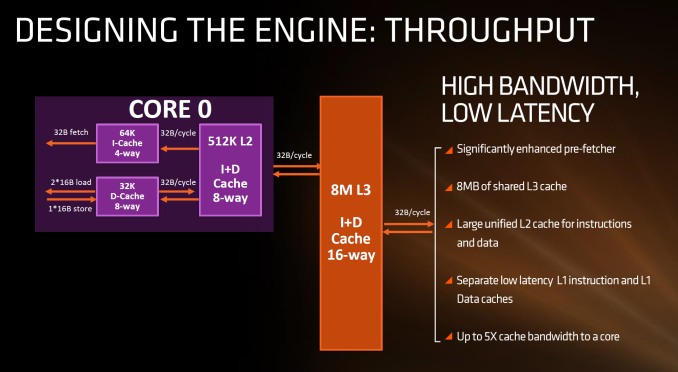
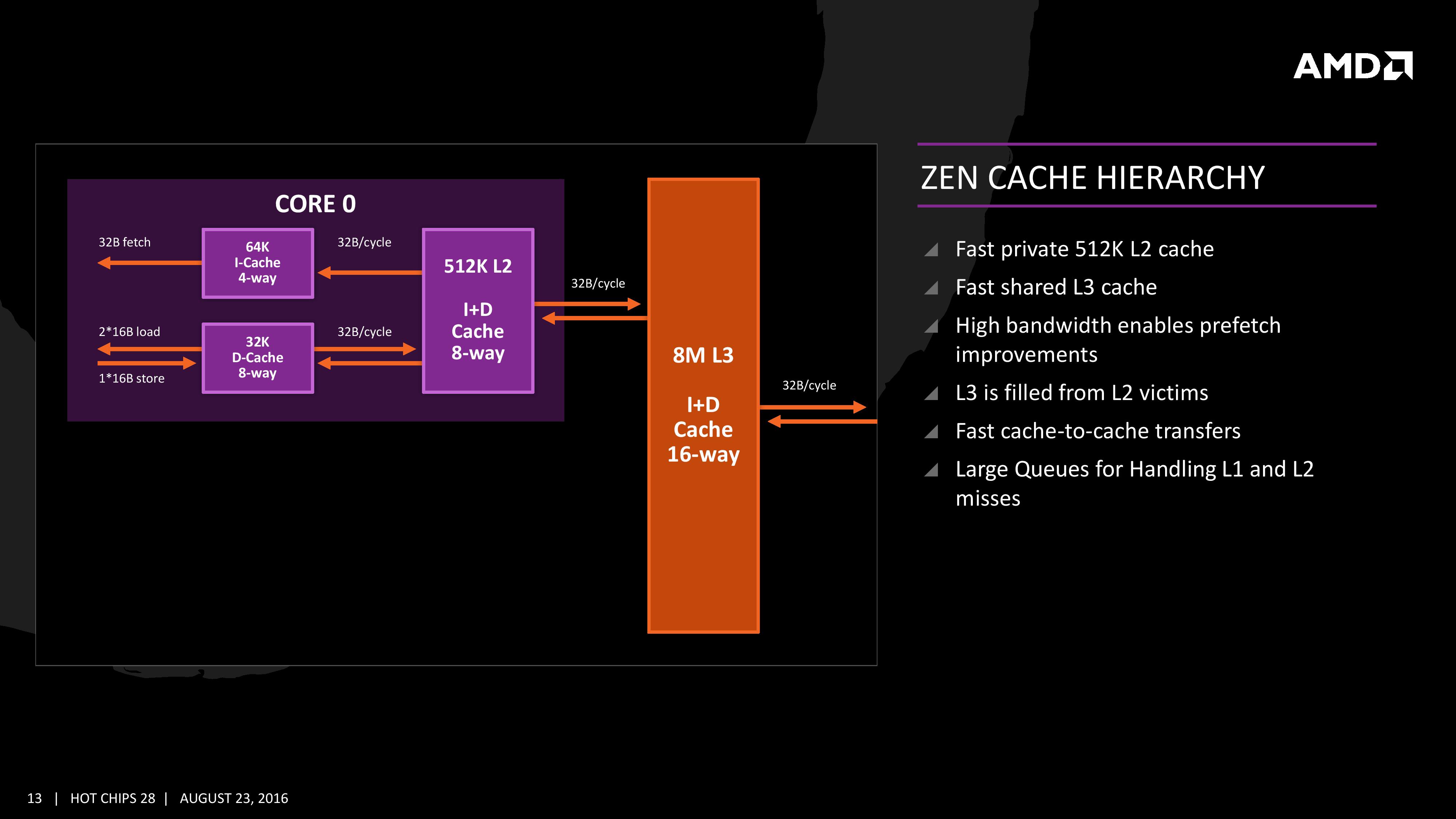
In this case, AMD has given Zen a 64KB L1 Instruction cache per core with 4-way associativity, with a lop-sided 32KB L1 Data cache per core with 8-way associativity. The size and accessibility determines how frequently a cache line is missed, and it is typically a trade-off for die area and power (larger caches require more die area, more associativity usually costs power). The instruction cache, per cycle, can afford a 32byte fetch while the data cache allows for 2x 16-byte loads and one 16-byte store per cycle. AMD stated that allowing two D-cache loads per cycle is more representative of the most workloads that end up with more loads than stores.
The L2 is a large 512 KB, 8-way cache per core. This is double the size of Intel’s 256 KB 4-way cache in Skylake or 256 KB 8-way cache in Broadwell. Typically doubling the cache size affords a 1.414 (square root of 2) better chance of a cache hit, reducing the need to go further out to find data, but comes at the expense of die area. This will have a big impact on a lot of performance metrics, and AMD is promoting faster cache-to-cache transfers than previous generations. Both the L1 and L2 caches are write-back caches, improving over the L1 write-through cache in Bulldozer.
The L3 cache is an 8MB 16-way cache, although at the time last week it was not specified over how many cores this was. From the data release today, we can confirm rumors that this 8 MB cache is split over a four-core module, affording 2 MB of L3 cache per core or 16 MB of L3 cache for the whole 8-core Zen CPU. These two 8 MB caches are separate, so act as a last-level cache per 4-core module with the appropriate hooks into the other L3 to determine if data is needed. As part of the talk today we also learned that the L3 is a pure victim cache for L1/L2 victims, rather than a cache for prefetch/demand data, which tempers the expectations a little but the large L2 will make up for this. We’ll discuss it as part of today’s announcement.
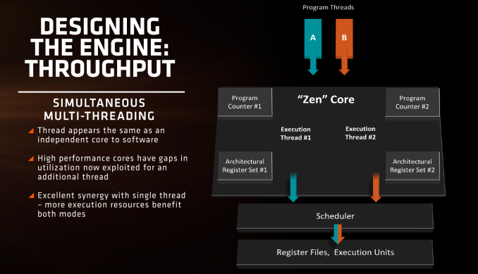
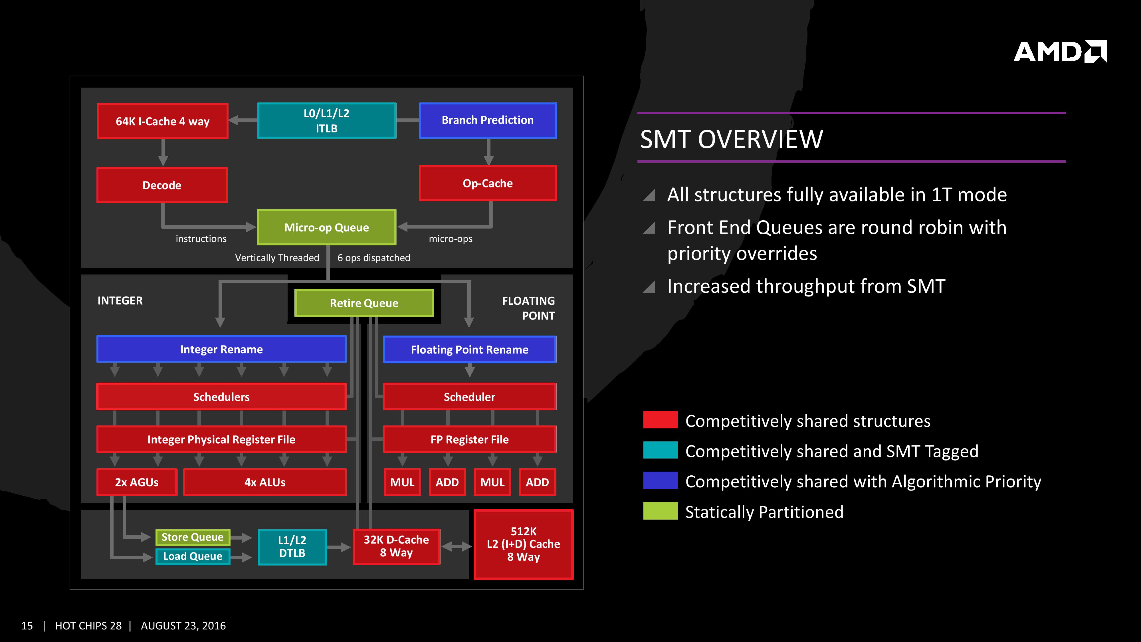
AMD is also playing with SMT, or simultaneous multi-threading. We’ve covered this with Intel extensively, under the heading ‘HyperThreading’. At a high level both these terms are essentially saying the same thing, although their implementations may differ. Adding SMT to a core design has the potential to increase throughput by allowing a second thread (or third, or fourth, or like IBM up to eight) on the same core to have the same access to execution ports, queues and caches. However SMT requires hardware level support – not all structures can be dynamically shared between threads and can either be algorithmically partitioned (prefetch), statically partitioned (micro-op queue) or used in alternate cycles (retire queue).
We also have dual schedulers, one for INT and another for FP, which is different to Intel’s joint scheduler/buffer implementation.
The Ryzen Die
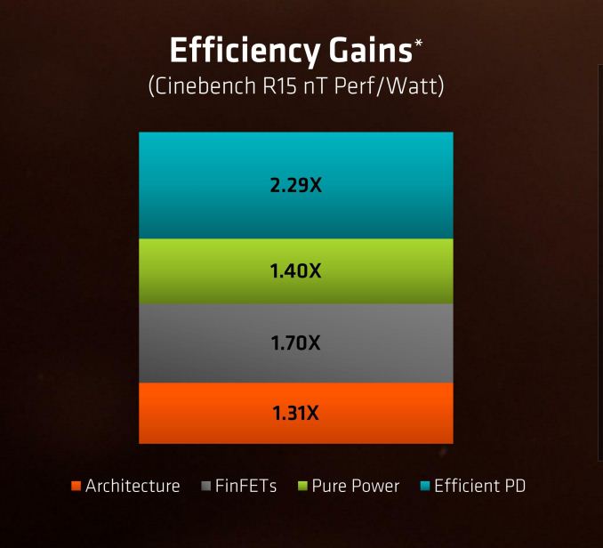
Throughout the time leading up to the launch of Ryzen, AMD reaffirmed its commitment to at least +40% IPC improvement over Excavator. This was specifically listed as a goal relating to performance, at an equivalent energy per cycle, resulting in a 40% increase in efficiency. At the Tech Day, AMD listed an overall 2.7x (or 270%) performance per watt improvement, split into the following:
Obviously a number of benefits come from moving the 28nm TSMC process to GloFo’s 14nm FinFET process which is used via a Samsung license. Both the smaller node and FinFET improvements have been well documented so we won’t go over them here, but AMD is stating that Zen is much more than this as a direct improvement to immediate performance, not just efficiency. While Zen is initially a high-performance x86 core at heart, it is designed to scale all the way from notebooks to supercomputers, or from where the Cat cores (such as Jaguar and Puma) were all the way up to the old Opterons and beyond, all with at least +40% IPC.
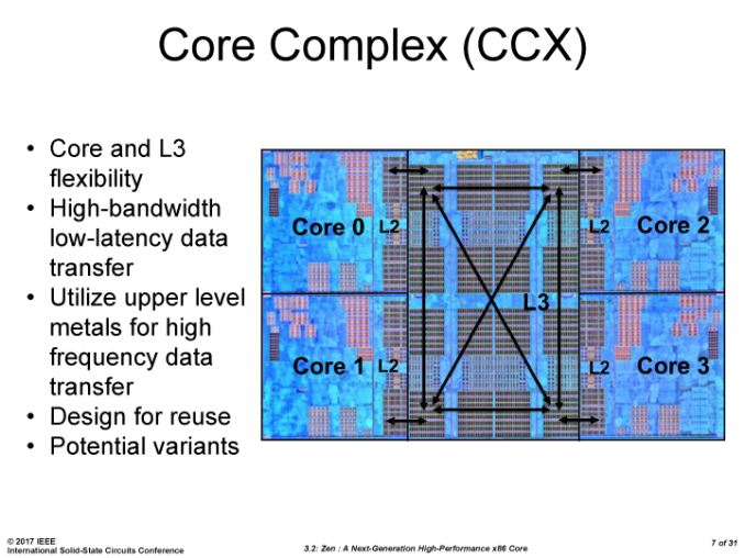
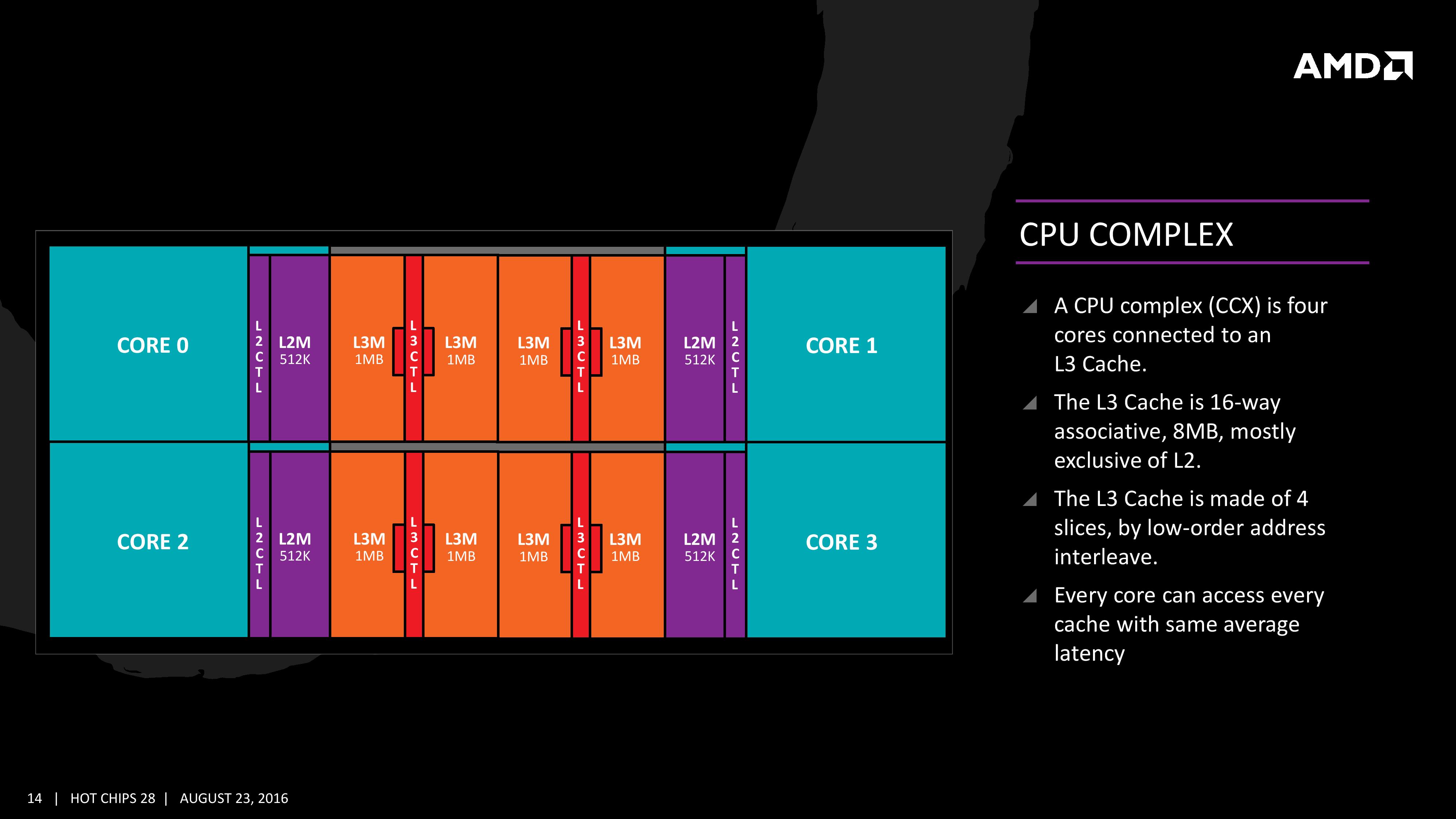
The first immediate image out of the presentation is the CPU Complex (a CCX), which shows the Zen core design as a four-CPU cluster with caches. This shows the L2/L3 cache breakdown, and also confirms 2MB of L3 per core with 8 MB of L3 per CCX. It also states that the L3 is mostly inclusive of the L2 cache, which stems from the L3 cache as a victim cache for L2 data. AMD is stating that the protocols involved in the L3 cache design allow each core to access the L3 of each other core with an average (but range) of latencies.
Over the next few pages, we’ll go through the slides. They detail more information about the application of Simultaneous Multithreading (SMT), New Instructions, the size of various queues and buffers, the back-end of the design, the front-end of the design, fetch, decode, execute, load/store and retire segments.
The High-Level Zen Overview
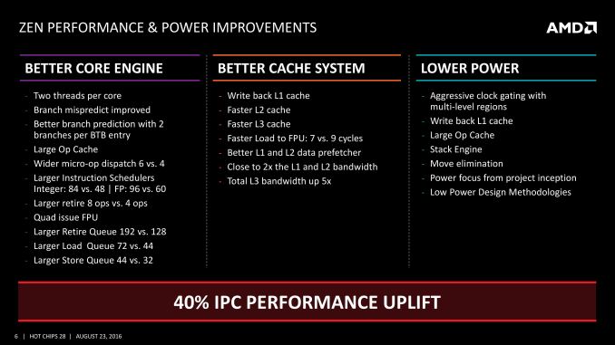
AMD is keen to stress that the Zen project had three main goals: core, cache and power. The power aspect of the design is one that was very aggressive – not in the sense of aiming for a mobile-first design, but efficiency at the higher performance levels was key in order to be competitive again. It is worth noting that AMD did not mention ‘die size’ in any of the three main goals, which is usually a requirement as well. Arguably you can make a massive core design to run at high performance and low latency, but it comes at the expense of die size which makes the cost of such a design from a product standpoint less economical (if AMD had to rely on 500mm2 die designs in consumer at 14nm, they would be priced way too high). Nevertheless, power was the main concern rather than pure performance or function, which have been typical AMD targets in the past. The shifting of the goal posts was part of the process to creating Zen.
This slide contains a number of features we will hit on later in this piece, but covers a number of main topics which come under those main three goals of core, cache and power.
For the core, having bigger and wider everything was to be expected, however maintaining a low latency can be difficult. Features such as the micro-op cache help most instruction streams improve in performance and bypass parts of potentially long-cycle repetitive operations, but also the larger dispatch, larger retire, larger schedulers and better branch prediction means that higher throughput can be maintained longer and in the fastest order possible. Add in dual threads and the applicability of keeping the functional units occupied with full queues also improves multi-threaded performance.
For the caches, having a faster prefetch and better algorithms ensures the data is ready when each of the caches when a thread needs it. Aiming for faster caches was AMD’s target, and while they are not disclosing latencies or bandwidth at this time, we are being told that L1/L2 bandwidth is doubled with L3 up to 5x.
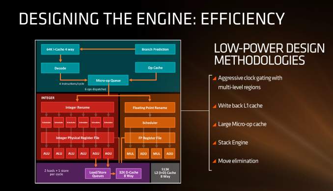
For the power, AMD has taken what it learned with Carrizo and moved it forward. This involves more aggressive monitoring of critical paths around the core, and better control of the frequency and power in various regions of the silicon. Zen will have more clock regions (it seems various parts of the back-end and front-end can be gated as needed) with features that help improve power efficiency, such as the micro-op cache, the Stack Engine (dedicated low power address manipulation unit) and Move elimination (low-power method for register adjustment - pointers to registers are adjusted rather than going through the high-power scheduler).
The Big Core Diagram
We saw this diagram last year, showing some of the bigger features AMD wants to promote:
The improved branch predictor allows for 2 branches per Branch Target Buffer (BTB), but in the event of tagged instructions will filter through the micro-op cache. On the other side, the decoder can dispatch 4 instructions per cycle however some of those instructions can be fused into the micro-op queue. Fused instructions still come out of the queue as two micro-ops, but take up less buffer space as a result.
As mentioned earlier, the INT and FP pipes and schedulers are separated, however the INT rename space is 168 registers wide, which feeds into 6x14 scheduling queues. The FP employs as 160 entry register file, and both the FP and INT sections feed into a 192-entry retire queue. The retire queue can operate at 8 instructions per cycle, moving up from 4/cycle in previous AMD microarchitectures.
The load/store units are improved, supporting a 72 out-of-order loads, similar to Skylake. We’ll discuss this a bit later. On the FP side there are four pipes (compared to three in previous designs) which support combined 128-bit FMAC instructions. These can be combined for one 256-bit AVX, but beyond that it has to be scheduled over multiple instructions.
Fetch
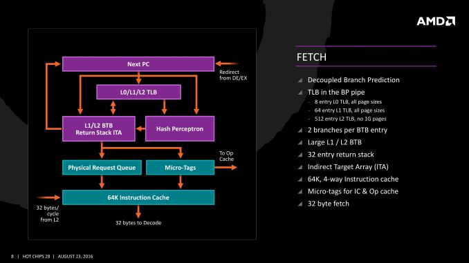
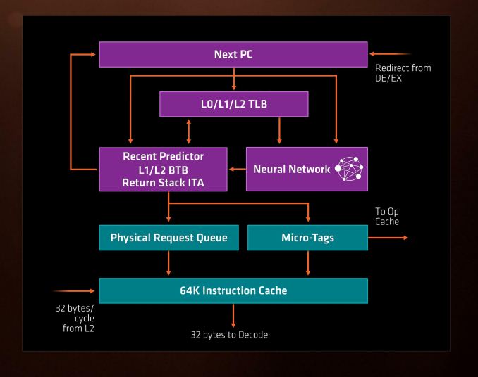
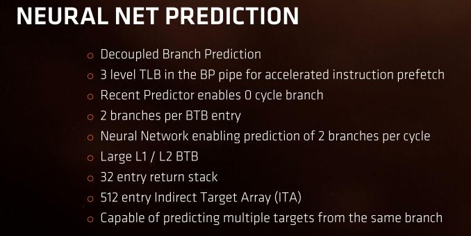
For Zen, AMD has implemented a decoupled branch predictor. This allows support to speculate on incoming instruction pointers to fill a queue, as well as look for direct and indirect targets. The branch target buffer (BTB) for Zen is described as ‘large’ but with no numbers as of yet, however there is an L1/L2 hierarchical arrangement for the BTB. For comparison, Bulldozer afforded a 512-entry, 4-way L1 BTB with a single cycle latency, and a 5120 entry, 5-way L2 BTB with additional latency; AMD doesn’t state that Zen is larger, just that it is large and supports dual branches. The 32 entry return stack for indirect targets is also devoid of entry numbers at this point as well.
The decoupled branch predictor also allows it to run ahead of instruction fetches and fill the queues based on the internal algorithms. Going too far into a specific branch that fails will obviously incur a power penalty, but successes will help with latency and memory parallelism.
The Translation Lookaside Buffer (TLB) in the branch prediction looks for recent virtual memory translations of physical addresses to reduce load latency, and operates in three levels: L0 with 8 entries of any page size, L1 with 64 entries of any page size, and L2 with 512 entries and support for 4K and 256K pages only. The L2 won’t support 1G pages as the L1 can already support 64 of them, and implementing 1G support at the L2 level is a more complex addition (there may also be power/die area benefits).
When the instruction comes through as a recently used one, it acquires a micro-tag and is set via the op-cache, otherwise it is placed into the instruction cache for decode. The L1-Instruction Cache can also accept 32 Bytes/cycle from the L2 cache as other instructions are placed through the load/store unit for another cycle around for execution.
Decode
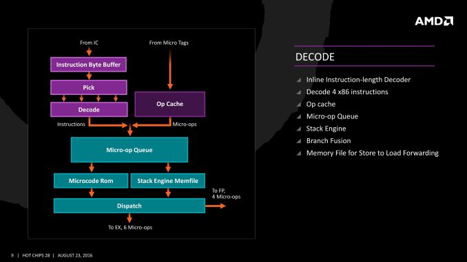
The instruction cache will then send the data through the decoder, which can decode four instructions per cycle. As mentioned previously, the decoder can fuse operations together in a fast-path, such that a single micro-op will go through to the micro-op queue but still represent two instructions, but these will be split when hitting the schedulers. The purpose of this allows the system to fit more into the micro-op queue and afford a higher throughput when possible.
The new Stack Engine comes into play between the queue and the dispatch, allowing for a low-power address generation when it is already known from previous cycles. This allows the system to save power from going through the AGU and cycling back around to the caches.
Finally, the dispatch can apply six instructions per cycle, at a maximum rate of 6/cycle to the INT scheduler or 4/cycle to the FP scheduler. We confirmed with AMD that the dispatch unit can simultaneously dispatch to both INT and FP inside the same cycle, which can maximize throughput (the alternative would be to alternate each cycle, which reduces efficiency). We are told that the operations used in Zen for the uOp cache are ‘pretty dense’, and equivalent to x86 operations in most cases.
Execution, Load/Store, INT and FP Scheduling
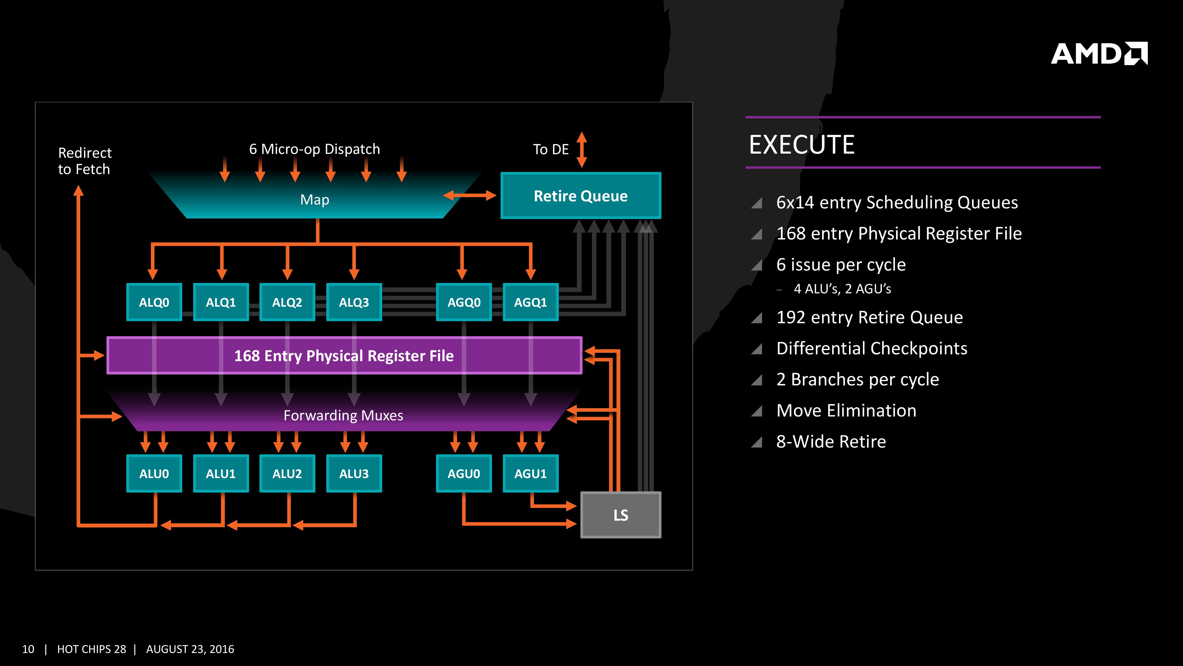
The execution of micro-ops get filters into the Integer (INT) and Floating Point (FP) parts of the core, which each have different pipes and execution ports. First up is the Integer pipe which affords a 168-entry register file which forwards into four arithmetic logic units and two address generation units. This allows the core to schedule six micro-ops/cycle, and each execution port has its own 14-entry schedule queue.
The INT unit can work on two branches per cycle, but it should be noted that not all the ALUs are equal. Only two ALUs are capable of branches, one of the ALUs can perform IMUL operations (signed multiply), and only one can do CRC operations. There are other limitations as well, but broadly we are told that the ALUs are symmetric except for a few focused operations. Exactly what operations will be disclosed closer to the launch date.
The INT pipe will keep track of branching instructions with differential checkpoints, to cut down on storing redundant data between branches (saves queue entries and power), but can also perform Move Elimination. This is where a simple mov command between two registers occurs – instead of inflicting a high energy loop around the core to physically move the single instruction, the core adjusts the pointers to the registers instead and essentially applies a new mapping table, which is a lower power operation.
Both INT and FP units have direct access to the retire queue, which is 192-entry and can retire 8 instructions per cycle. In some previous x86 CPU designs, the retire unit was a limiting factor for extracting peak performance, and so having it retire quicker than dispatch should keep the queue relatively empty and not near the limit.
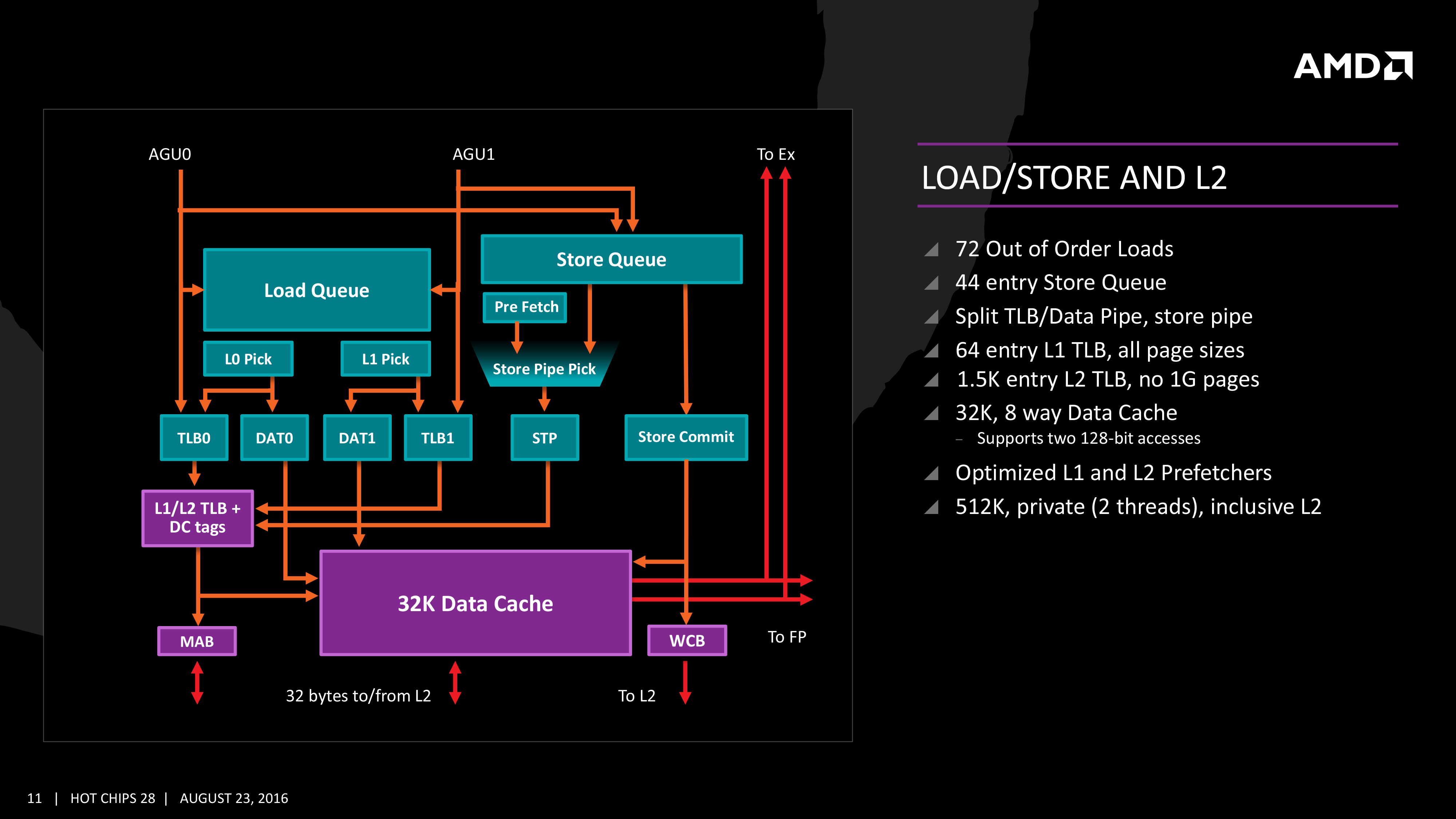
The Load/Store Units are accessible from both AGUs simultaneously, and will support 72 out-of-order loads. Overall, as mentioned before, the core can perform two 16B loads (2x128-bit) and one 16B store per cycle, with the latter relying on a 44-entry Store queue. The TLB buffer for the L2 cache for already decoded addresses is two level here, with the L1 TLB supporting 64-entry at all page sizes and the L2 TLB going for 1.5K-entry with no 1G pages. The TLB and data pipes are split in this design, which relies on tags to determine if the data is in the cache or to start the data prefetch earlier in the pipeline.
The data cache here also has direct access to the main L2 cache at 32 Bytes/cycle, with the 512 KB 8-way L2 cache being private to the core and inclusive. When data resides back in L1 it can be processed back to either the INT or the FP pipes as required.
Moving onto the floating point part of the core, and the first thing to notice is that there are two scheduling queues here. These are listed as ‘schedulable’ and ‘non-schedulable’ queues with lower power operation when certain micro-ops are in play, but also allows the backup queue to sort out parts of the dispatch in advance via the LDCVT. The register file is 160 entry, with direct FP to INT transfers as required, as well as supporting accelerated recovery on flushes (when data is written to a cache further back in the hierarchy to make room).
The FP Unit uses four pipes rather than three on Excavator, and we are told that the latency in Zen is reduced as well for operations (though more information on this will come at a later date). We have two MUL and two ADD in the FP unit, capable of joining to form two 128-bit FMACs, but not one 256-bit AVX. In order to do AVX, the unit will split the operations accordingly. On the counter side each core will have 2 AES units for cryptography as well as decode support for SSE, AVX1/2, SHA and legacy mmx/x87 compliant code.
The Core Complex, Caches, and Fabric
Many core designs often start with an initial low-core-count building block that is repeated across a coherent fabric to generate a large number of cores and the large die. In this case, AMD is using a CPU Complex (CCX) as that building block which consists of four cores and the associated caches.
Each core will have direct access to its private L2 cache, and the 8 MB of L3 cache is, despite being split into blocks per core, accessible by every core on the CCX with ‘an average latency’ also L3 hits nearer to the core will have a lower latency due to the low-order address interleave method of address generation.
The L3 cache is actually a victim cache, taking data from L1 and L2 evictions rather than collecting data from prefetch/demand instructions. Victim caches tend to be less effective than inclusive caches, however Zen counters this by having a sufficiency large L2 to compensate. The use of a victim cache means that it does not have to hold L2 data inside, effectively increasing its potential capacity with less data redundancy.
It is worth noting that a single CCX has 8 MB of cache, and as a result the 8-core Zen being displayed by AMD at the current events involves two CPU Complexes. This affords a total of 16 MB of L3 cache, albeit in two distinct parts. This means that the true LLC for the entire chip is actually DRAM, although AMD states that the two CCXes can communicate with each other through the custom fabric which connects both the complexes, the memory controller, the IO, the PCIe lanes etc.
The cache representation shows L1 and L2 being local to each the core, followed by 8MB of L3 split over several cores. AMD states that the L1 and L2 bandwidth is nearly double that of Excavator, with L3 now up to 5x for bandwidth, and that this bandwidth will help drive the improvements made on the prefetch side. AMD also states that there are large queues in play for L1/L2 cache misses.
One interesting story is going to be how AMD’s coherent fabric works. For those that follow mobile phone SoCs, we know fabrics and interconnects such as CCI-400 or the CCN family are optimized to take advantage of core clusters along with the rest of the chip. A number of people have speculated that the fabric used in AMD’s new design is based on HyperTransport, however AMD has confirmed that they are using a superset HyperTransport here for Zen, and that the Infinity fabric design is meant to be high bandwidth, low latency, and be in both Zen and Vega as well as future products. Almost similar to the CPU/GPU roadmaps, the Fabric has its own as well.
Ultimately the new fabric involves a series of control and data passing structures, with the data passing enabling third-party IP in custom designs, a high-performance common bus for large multi-unit (CPU/GPU) structures, and socket to socket communication. The control elements are an extension of power management, enabling parts of the fabric to duty cycle when not in use, security by way of memory management and detection, and test/initialization for activities such as data prefetch.
Simultaneous MultiThreading (SMT)
Zen will be AMD’s first foray into a true simultaneous multithreading structure, and certain parts of the core will act differently depending on their implementation. There are many ways to manage threads, particularly to avoid stalls where one thread is blocking another that ends in the system hanging or crashing. The drivers that communicate with the OS also have to make sure they can distinguish between threads running on new cores or when a core is already occupied – to achieve maximum throughput then four threads should be across two cores, but for efficiency where speed isn’t a factor, perhaps power gating/clock gating half the cores in a CCX is a good idea.
There are a number of ways that AMD will deal with thread management. The basic way is time slicing, and giving each thread an equal share of the pie. This is not always the best policy, especially when you have one performance dominant thread, or one thread that creates a lot of stalls, or a thread where latency is vital. In some methodologies the importance of a thread can be tagged or determined, and this is what we get here, though for some of the structures in the core it has to revert to a basic model.
With each thread, AMD performs internal analysis on the data stream for each to see which thread has algorithmic priority. This means that certain threads will require more resources, or that a branch miss needs to be prioritized to avoid long stall delays. The elements in blue (Branch Prediction, INT/FP Rename) operate on this methodology.
A thread can also be tagged with higher priority. This is important for latency sensitive operations, such as a touch-screen input or immediate user input elements required. The Translation Lookaside Buffers work in this way, to prioritize looking for recent virtual memory address translations. The Load Queue is similarly enabled this way, as typically low latency workloads require data as soon as possible, so the load queue is perfect for this.
Certain parts of the core are statically partitioned, giving each thread an equal timing. This is implemented mostly for anything that is typically processed in-order, such as anything coming out of the micro-op queue, the retire queue and the store queue. However, when running in SMT mode but only with a single thread, the statically partitioned parts of the core can end up as a bottleneck, as they are idle half the time.
The rest of the core is done via competitive scheduling, meaning that if a thread demands more resources it will try to get there first if there is space to do so each cycle.
New Instructions
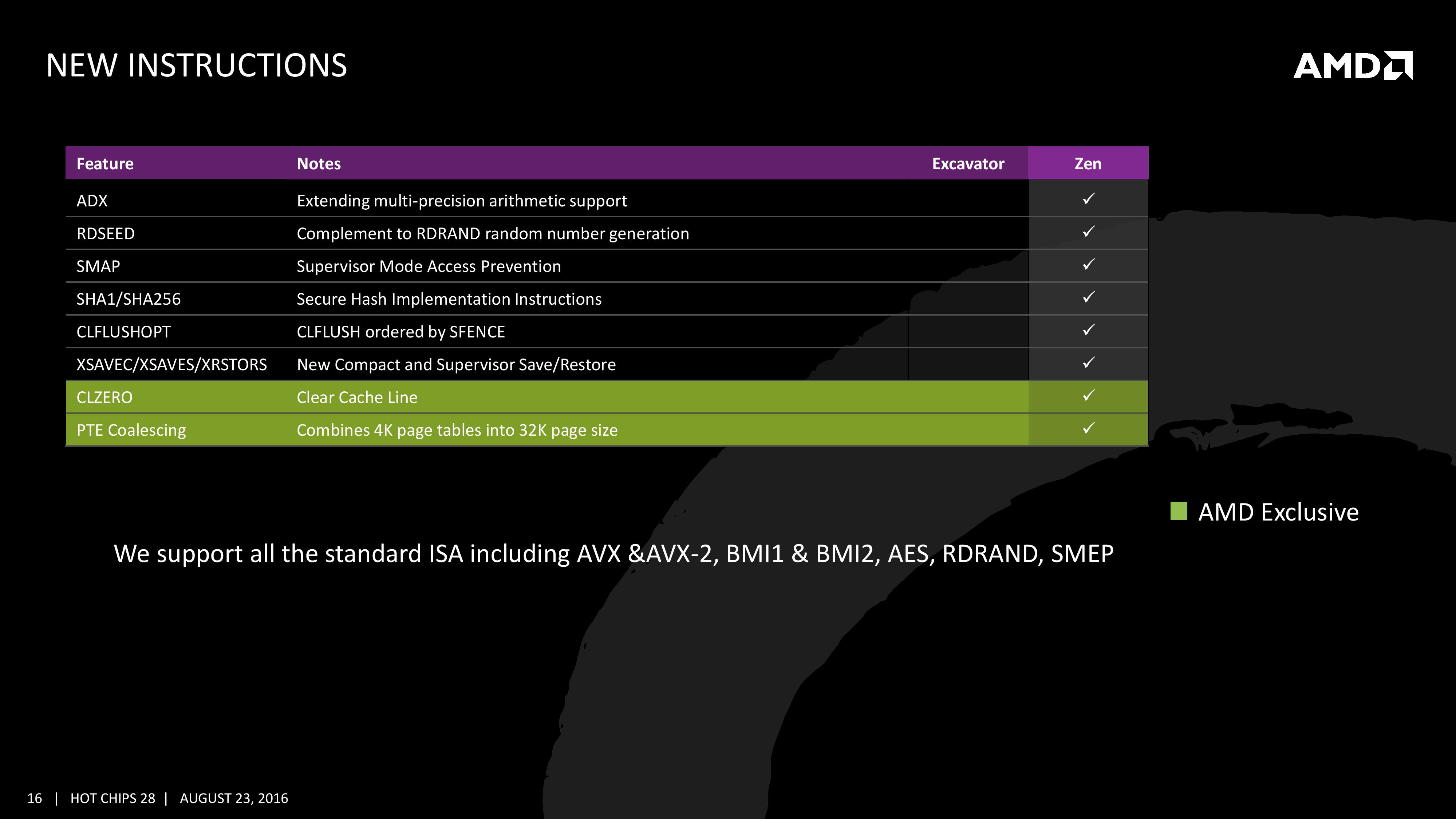
AMD has a couple of tricks up its sleeve for Zen. Along with including the standard ISA, there are a few new custom instructions that are AMD only.
Some of the new commands are linked with ones that Intel already uses, such as RDSEED for random number generation, or SHA1/SHA256 for cryptography (even with the recent breakthrough in security). The two new instructions are CLZERO and PTE Coalescing.
The first, CLZERO, is aimed to clear a cache line and is more aimed at the data center and HPC crowds. This allows a thread to clear a poisoned cache line atomically (in one cycle) in preparation for zero data structures. It also allows a level of repeatability when the cache line is filled with expected data. CLZERO support will be determined by a CPUID bit.
PTE (Page Table Entry) Coalescing is the ability to combine small 4K page tables into 32K page tables, and is a software transparent implementation. This is useful for reducing the number of entries in the TLBs and the queues, but requires certain criteria of the data to be used within the branch predictor to be met.
Power, Performance, and Pre-Fetch: AMD SenseMI
Part of the demos leading up to the launch involved a Handbrake video transcode: a multithreaded test, showing a near-identical completion time between a high-frequency Ryzen without turbo compared to an i7-6900K at similar frequencies. Similarly we saw a Blender test we saw back in August achieving the same feat. AMD at the time also fired up some power meters, showing that Ryzen power consumption in that test was a few watts lower than the Intel part, implying that AMD is meeting its targets for power, performance and as a result, efficiency. The 52% improvement in IPC/efficiency is a result AMD seems confident that this target has been surpassed.
Leading up to the launch, AMD explained during our briefings that during the Zen design stages, up to 300 engineers were working on the core engine with an aggressive mantra of higher IPC for no power gain. This has apparently lead to over two million work hours of time dedicated to Zen. This is not an uncommon strategy for core designs. Part of this time will be spent devoping new power modes, and part of Zen is is that optimization and extension of the power/frequency curve: a key point in AMD’s new 5-stage ‘SenseMI’ technology.
SenseMI Stage 1: Pure Power
A number of recent microprocessor launches have revolved around silicon-optimized power profiles. We are now removed from the ‘one DVFS curve fits all’ application for high-end silicon, and AMD’s solution in Ryzen will be called Pure Power. The short explanation is that using distributed embedded sensors in the design (first introduced in bulk with Carrizo) that monitor temperature, speed and voltage, and the control center can manage the power consumption in real time. The glue behind this technology comes in form of AMD’s new ‘Infinity Fabric’.
The fact that it’s described as a fabric means that it goes through the entire processor, connecting various parts together as part of that control. This is something wildly different to what we saw in Carrizo, aside from being the next-gen power adjustment and under a new name, and will permiate through Zen, Vega, and future AMD products.
The upshot of Pure Power is that the DVFS curve is lower and more optimized for a given piece of silicon than a generic DVFS curve, which results in giving lower power at various/all levels of performance. This in turn benefits the next part of SenseMI, Precision Boost.
SenseMi Stage 2: Precision Boost
For almost a decade now, most commercial PC processors have invoked some form of boost technology to enable processors to use less power when idle and fully take advantage of the power budget when only a few elements of the core design is needed. We see processors that sit at 2.2 GHz that boost to 2.7 GHz when only one thread is needed, for example, because the whole chip still remains under the power limit. AMD is implementing Precision Boost for Ryzen, increasing the DVFS curve to better performance due to Pure Power, but also offering frequency jumps in 25 MHz steps which is new.
Precision Boost relies on the same Infinity Control Fabric that Pure Power does, but allows for adjustments of core frequency based on performance requirements and suitability/power given the rest of the core. The fact that it offers 25 MHz steps is surprising, however.
Current turbo control systems, on both AMD and Intel, are invoked by adjusting the CPU frequency multiplier. With the 100 MHz base clock on all modern CPUs, one step in frequency multiplier gives 100 MHz jump for the turbo modes, and any multiple of the multiplier can be used on the basis of whole numbers only.
With AMD moving to 25 MHz jumps in their turbo, this means either AMD can implement 0.25x fractional multipliers, similar to how processors in the early 2000s were able to negotiate 0.5x multiplier jumps. What this means in reality is that the processor has over 100 different frequencies it can potentially operate at, although control of the fractional multipliers below P0 is left to XFR (below).
Part of this comes down to the extensive sensor technology, originally debuted for AMD in Carrizo at scale, but now offering almost 1000 sensors per chip to analyze at what frequency the core can run at. AMD controls all frequency of each core independently, which suggests that users might be able to find the highest performing core and lock important software on it.
If we consider that Zen’s original chief designer was Jim Keller (and his team), known for a number of older generation of AMD processors, a similar fractional multiplier technology might be in play here. If/when we get more information on it, we will let you know.
SenseMi Stage 3: Extended Frequency Range (XFR)
The main marketing points of on-the-fly frequency adjustment are typically down to low idle power and higher performance when needed. The current processors on the market have rated speeds on the box which are fixed frequency settings that can be chosen by the processor/OS depending on what level of performance is possible/required. AMD’s new XFR mode seems to do away with this, offering what sounds like an unlimited bound on performance.
The concept here is that, beyond the rated turbo mode, if there is sufficient cooling then the CPU will continue to increase the clock speed and voltage until a cooling limit is reached. This is somewhat murky territory, though AMD claims that a multitude of different environments can be catered for the feature. AMD was not clear if this limit is determined by power consumption, temperature, or if they can protect from issues such as a bad frequency/voltage setting.
This is a dynamic adjustment rather than just another embedded look-up table such as P-states. AMD states that XFR is a fully automated system with no user intervention, although I suspect in time we might see an on/off switch in the BIOS. It also somewhat negates overclocking if your cooling can support it, which then brings up the issue for overclocking in general: casual users may not ever need to step into the overclocking world if the CPU does it all automatically.
I imagine that a manual overclock will still be king, especially for extreme overclockers competing with liquid nitrogen, as being able to personally fine tune a system might be better than letting the system do it itself. It can especially be true in those circumstances, as sensors on hardware can fail, report the wrong temperature, or may only be calibrated within a certain range.
XFR will be on every consumer CPU (as the Zen microarchitecture is destined for server and mobile as well, XFR might have different connotations for both of those markets), and typically will allow for +100 MHz. CPUs that have the extra 'X' should allow for up to +200 MHz through XFR. This level of XFR is not set in stone, and may change in future CPUs.
SenseMi Stage 4+5: Neural Net Prediction and Smart Prefetch
Every generation of CPUs from the big companies come with promises of better prediction and better pre-fetch models. These are both important to hide latency within a core which might be created by instruction decode, queuing, or more usually, moving data between caches and main memory to be ready for the instructions. With Ryzen, AMD is introducing its new Neural Net Prediction hardware model along with Smart Pre-Fetch.
AMD is announcing this as a ‘true artificial network inside every Zen processor that builds a model of decisions based on software execution’. This can mean one of several things, ranging from actual physical modelling of instruction workflow to identify critical paths to be accelerated (unlikely) or statistical analysis of what is coming through the engine and attempting to work during downtime that might accelerate future instructions (such as inserting an instruction to decode into an idle decoder in preparation for when it actually comes through, therefore ends up using the micro-op cache and making it quicker).
For Zen this means two branches can be predicted per cycle (so, one per thread per cycle), and a multi-level TLB to assist recently required instructions again. With these caches and buffers, typically doubling in size gets a hit rate of sqrt(2), or +41%, for double the die area, and it becomes a balance of how good you want it to be compared with how much floor plan area can be dedicated to it.
Modern processors already do decent jobs when repetitive work is being used, such as identifying when every 4th element in a memory array is being accessed, and can pull that data in earlier to be ready in case it is used. The danger of smart predictors however is being overly aggressive – pulling in too much data that old data might be ditched because it’s never used (over prediction), pulling in too much data such that it’s already evicted by the time the data is needed (aggressive prediction), or simply wasting excess power with bad predictions (stupid prediction…).
AMD is stating that Zen implements algorithm learning models for both instruction prediction and prefetch, which will no doubt be interesting to see if they have found the right balance of prefetch aggression and extra work in prediction.
It is worth noting here that AMD will likely draw upon the increased L3 bandwidth in the new core as a key element to assisting the prefetch, especially as the shared L3 cache is an exclusive victim cache and designed to contain data already used/evicted to be used again at a later date.
Thoughts and Comparisons
Throughout AMD's road to releasing details on Zen, we have had a chance to examine the information on the microarchitecture often earlier than we had expected to each point in the Zen design/launch cycle. Part of this is due to the fact that internally, AMD is very proud of their design, but some extra details (such as the extent of XFR, or the size of the micro-op cache), AMD has held close to its chest until the actual launch. With the data we have at hand, we can fill out a lot of information for a direct comparison chart to AMD’s last product and Intel’s current offerings.
| CPU uArch Comparison | ||||
| AMD | Intel | |||
| Zen 8C/16T 2017 |
Bulldozer 4M / 8T 2010 |
Skylake Kaby Lake 4C / 8T 2015/7 |
Broadwell 8C / 16T 2014 |
|
| L1-I Size | 64KB/core | 64KB/module | 32KB/core | 32KB/core |
| L1-I Assoc | 4-way | 2-way | 8-way | 8-way |
| L1-D Size | 32KB/core | 16KB/thread | 32KB/core | 32KB/core |
| L1-D Assoc | 8-way | 4-way | 8-way | 8-way |
| L2 Size | 512KB/core | 1MB/thread | 256KB/core | 256KB/core |
| L2 Assoc | 8-way | 16-way | 4-way | 8-way |
| L3 Size | 2MB/core | 1MB/thread | >2MB/cire | 1.5-3MB/core |
| L3 Assoc | 16-way | 64-way | 16-way | 16/20-way |
| L3 Type | Victim | Victim | Write-back | Write-back |
| L0 ITLB Entry | 8 | - | - | - |
| L0 ITLB Assoc | ? | - | - | - |
| L1 ITLB Entry | 64 | 72 | 128 | 128 |
| L1 ITLB Assoc | ? | Full | 8-way | 4-way |
| L2 ITLB Entry | 512 | 512 | 1536 | 1536 |
| L2 ITLB Assoc | ? | 4-way | 12-way | 4-way |
| L1 DTLB Entry | 64 | 32 | 64 | 64 |
| L1 DTLB Assoc | ? | Full | 4-way | 4-way |
| L2 DTLB Entry | 1536 | 1024 | - | - |
| L2 DTLB Assoc | ? | 8-way | - | - |
| Decode | 4 uops/cycle | 4 Mops/cycle | 5 uops/cycle | 4 uops/cycle |
| uOp Cache Size | 2048 | - | 1536 | 1536 |
| uOp Cache Assoc | ? | - | 8-way | 8-way |
| uOp Queue Size | ? | - | 128 | 64 |
| Dispatch / cycle | 6 uops/cycle | 4 Mops/cycle | 6 uops/cycle | 4 uops/cycle |
| INT Registers | 168 | 160 | 180 | 168 |
| FP Registers | 160 | 96 | 168 | 168 |
| Retire Queue | 192 | 128 | 224 | 192 |
| Retire Rate | 8/cycle | 4/cycle | 8/cycle | 4/cycle |
| Load Queue | 72 | 40 | 72 | 72 |
| Store Queue | 44 | 24 | 56 | 42 |
| ALU | 4 | 2 | 4 | 4 |
| AGU | 2 | 2 | 2+2 | 2+2 |
| FMAC | 2x128-bit | 2x128-bit 2x MMX 128-bit |
2x256-bit | 2x256-bit |
Bulldozer uses AMD-coined macro-ops, or Mops, which are internal fixed length instructions and can account for 3 smaller ops. These AMD Mops are different to Intel's 'macro-ops', which are variable length and different to Intel's 'micro-ops', which are simpler and fixed-length.
Excavator has a number of improvements over Bulldozer, such as a larger L1-D cache and a 768-entry L1 BTB size, however we were never given a full run-down of the core in a similar fashion and no high-end desktop version of Excavator will be made.
This isn’t an exhaustive list of all features (thanks to CPU World, Real World Tech and WikiChip for filling in some blanks) by any means, and doesn’t paint the whole story. For example, on the power side of the equation, AMD is stating that it has the ability to clock gate parts of the core and CCX that are not required to save power, and the L3 runs on its own clock domain shared across the cores. Or the latency to run certain operations, which is critical for workflow if a MUL operation takes 3, 4 or 5 cycles to complete. We have been told that the FPU load is two cycles quicker, which is something. The latency in the caches is also going to feature heavily in performance, and all we are told at this point is that L2 and L3 are lower latency than previous designs.
A number of these features we’ve already seen on Intel x86 CPUs, such as move elimination to reduce power, or the micro-op cache. The micro-op cache is a piece of the puzzle we wanted to know more about from day one, especially the rate at which we get cache hits for a given workload. Also, the use of new instructions will adjust a number of workloads that rely on them. Some users will lament the lack of true single-instruction AVX-2 support, however I suspect AMD would argue that the die area cost might be excessive at this time. That’s not to say AMD won’t support it in the future – we were told quite clearly that there were a number of features originally listed internally for Zen which didn’t make it, either due to time constraints or a lack of transistors.
We are told that AMD has a clear internal roadmap for CPU microarchitecture design over the next few generations. As long as we don’t stay for so long on 14nm similar to what we did at 28/32nm, with IO updates over the coming years, a competitive clock-for-clock product (even to Broadwell) with good efficiency will be a welcome return.
Chipsets and Motherboards: 300-series and AM4
Users keeping tabs on the developments of CPUs will have seen the shift over the last ten years to moving the traditional ‘northbridge’ onto the main CPU die. The northbridge was typically the connectivity hub, allowing the CPU to communicate to the PCIe, DRAM and the Chipset (or Southbridge), and moving this onto the CPU silicon gave better latency, better power characteristics, and reduced the complexity of the motherboard, all for a little extra die area. Typically when we say ‘CPU’ in the context of a modern PC build, this is the image we have, with the CPU containing cores and possibly graphics (which AMD calls an APU).
Typically the CPU/APU has limited connectivity: video outputs (if an integrated GPU is present), a PCIe root complex for the main PCIe lanes, and an additional connectivity pathway to the chipset to enable additional input/output functionality. The chipset uses a one-to-many philosophy, whereby the total bandwidth between the CPU and Chipset may be lower than the total bandwidth of all the functionality coming out of the chipset. Using FIFO buffers, this is typically managed as required. The best analogy for this is that a motorway is not 50 million lanes wide, because not all cars use it at the same time. You only need a few lanes to cater for all but the busiest circumstances.
If the CPU also has the chipset/southbridge built in, either in the silicon or as a multi-chip package, we typically call this an ‘SoC’, or system on chip, as the one unit has all the connectivity needed to fully enable its use. Add on some slots, some power delivery and firmware, then away you go.
Platform = SoC + Chipset (Optional)
The AM4 platform will cater for both Ryzen CPUs (Summit Ridge, SR) and the second generation of Excavator APUs (Bristol Ridge, BR). As a result, the capabilities of the two have share some commonality in order to be interoperable with the same motherboard products. As a result, there is only a few minor differences:
Here is Bristol Ridge, with eight PCIe 3.0 lanes for add-in cards, two SATA 6 Gbps, four USB 3.0 ports, two PCIe x1 lanes, and a PCIe x4 lane for the chipset. The chipset is optional, as those four lanes could be put to use elsewhere (or bifurcated into x1/x1/x2 as required) when extra IO is not needed.
What differs with Ryzen and Summit Ridge is numbers: sixteen lanes for add-in cards and four SATA 6 Gbps ports plus an x2 NVMe (or two SATA plus an x4 NVMe). What AMD is doing with AM4 is a half-way house between a SoC and having a fully external chipset. Some of the connectivity, such as SATA ports, PCIe storage, or PCIe lanes beyond the standard GPU lanes, is built into the processor. These fall under the features of the processor, and for the current launch is a fixed set of features. The CPU also has additional connectivity to an optional chipset which can provide more features, however the use of the chipset is optional.
PCIe is Fun with Switches: PLX, Thunderbolt, 10GigE, the Kitchen Sink
Another thing about the x16 link or x8/x8 links, rather than say a total of 28/40 lanes, is that it can be combined with an external PCIe switch. In my discussions with AMD, they suggested a switch that bifurcates a x8 to dual x4 interfaces, which could leverage fast PCIe storage while maintaining the onboard graphics for any GPU duties. There’s the other side, in using an x16 or x8 to x32 PCIe switch and affording two large x16 links.
Here’s a crazy mockup I thought of, using a $100 PCIe switch. I doubt this would come to market.
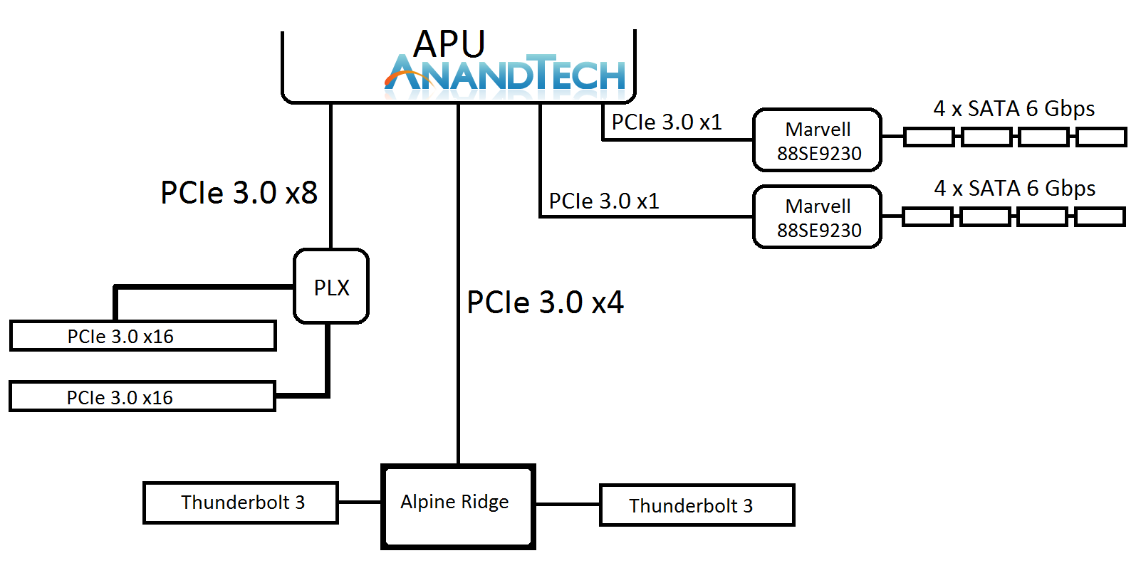
Ian plays a crazy game of PCIe Lego
The joy of PCIe and switches is that it becomes a mix and match game - there’s also the PCIe 3.0 x4 to the chipset. This can be used for non-chipset duties, such as anything that takes PCIe 3.0 x4 like a fast SSD, or potentially Thunderbolt 3. We discussed TB3 support, via Intel’s Alpine Ridge controller, and we were told that the AM4 platform is currently being validated for systems supporting AMD XConnect, which will require Thunderbolt support. AMD did state that they are not willing to speculate on TB3 use, and from my perspective this is because the external GPU feature is what AMD is counting on as being the primary draw for TB3 enabled systems (particularly for OEMs). I suspect the traditional motherboard manufacturers will offer wilder designs, and ASRock likes to throw some spaghetti at the wall, to see what sticks.
The AM4 Socket
One of the common perceptions of AMD is that they like to keep a socket for many, many generations. Both AM3/3+ and FM2/2+ have existed for at least three generations of CPUs a piece, and the main thinking here is that backwards compatibility was important. Because Ryzen requires DDR4 memory, enables PCIe, and perhaps some other magic, more pins and a new socket is needed, breaking that trend. The new CPU uses 1331 pins, up from the 939-941 we’ve had before, but essentially in the same dimensions, meaning that the pins are smaller and now easier to break / accidentally smear thermal grease into and not be able to get it out.
The socket then changes to accommodate the pins, however AMD is still using a zero insertion force (ZIF) method for contact. Which means every so often, if I have a good seal between the CPU and the heatsink, removing the heatsink also removes the CPU – not a critical issue, but not the preferred state of things.
The socket hole mounting does change however, from AM3 to AM4. On AM3 the dimensions were, center hole to center hole, 96mm x 48mm. This led to a very cumbersome rectangular design for sure. AM4 makes the design more square, down to 90mm x 54mm, but is still very square. With the new mounting holes, users will need brackets for existing CPU coolers or buy new coolers with the new brackets. More on that in a second.
It is worth noting that AMD has still kept the same mounting mechanism from AM3 for coolers that use a spring loaded mount on AMD’s plastic clips. So users with a spring loaded mount cooler, will still be able to use it as the plastic clip on the new boards is in the right place. Some motherboard manufacturers are also taking the initiative, and implementing both sets of AM3 and AM4 hole mounts such that the older coolers will be able to be used. However, using an older cooler might result in a few issues depending on the screw height, as reviewers have already been complaining about bad contact. In our review today, we used a Noctua DH-U12S SE-AM4 cooler that implements rails and then a secondary screw system, and it has none of the issues we just described. Ultimately all motherboards will end up just with AM4 holes, but it should facilitate smaller form factor motherboards where AM3 was perhaps too rectangular.
| Coolers Supporting AMD Ryzen Processors in AM4 Form-Factor | ||||||
| Manufacturer | Already Compatible |
Requires New Mounting Kit |
Upcoming | |||
| ARCTIC | Alpine 64 Plus Alpine 64 Pro Alpine 64 GT Freezer 7 Pro Freezer 13 Freezer 13 Limited Freezer 13 CO Freezer Extreme |
Liquid Freezer 120/240/360 (kit to be available in April) | Freezer 12 Freezer 33 |
|||
| Be Quiet! | Pure Rock Pure Rock Slim Shadow Rock LP |
Dark Rock 3 Dark Rock Pro 3 Dark Rock TF Shadow Rock 2 Shadow Rock Slim Silent Loop |
||||
| Corsair | H60 H110i H100i |
All the remaining Hydro coolers. Customers can claim their retention bracket here for free, no proof of purchase is required. |
||||
| Cryorig | - | C1 R1 Universal/Ultimate H5 Universal/Ultimate H7 H7 Quad Lumi M9a C7 A40 A40 Ultimate A80 |
||||
| Cooler Master | MasterLiquid 240 MasterLiquid 120 MasterLiquid Lite 120 Hyper 212 LED Turbo Hyper T4 Hyper TX3 (Plastics) Hyper TX3 EVO (EU Ver.) Hyper TX3 EVO (JP Ver.) Hyper TX3 EVO Hyper T2 Hyper 101 PWM U BLIZZARD T2 BLIZZARD T2 MINI |
MasterLiquid Pro Series Nepton Series Seidon Series MasterAir Maker 8 MasterAir Pro 4 MasterAir Pro 3 Hyper 612 Ver.2 Hyper 412 Series Hyper 212 LED Hyper 212 EVO Hyper 212 X Hyper D92 |
||||
| DeepCool | Beta 10 Beta 200ST CK0AM209 Gammaxx Gamma Archer Ice Blade 100 Ice Blade 200M Ice Edge Mini FS 2.0 |
Assassin II Beta 11 Beta 40 Captain Series Frostwin Series Gabriel HTPC-200 Ice Blade Pro 2.0 Lucifer Series Maelstrom Series Neptwin Series |
||||
| Enermax | ETS-T50A-BVT ETS-T50A-WVS ETS-T40F-TB ETS-T40F-BK ETS-T40F-W ETS-T40F-RF ETS-N30R-HE ETS-N30R-TAA ELC-LMR240-BS ELC-LMR120S-BS |
|||||
| MSI | Core Frozr L | |||||
| Noctua | NH-D15 SE-AM4 NH-U12S SE-AM4 NH-L9x65 SE-AM4 |
NH-C12P NH-C12P SE14 NH-C14 NH-C14S NH-D14 NH-D14 SE2011 NH-D15 NH-D15S NH-D9L NH-L12 NH-L9x65 NH-U12 NH-U12F NH-U12P NH-U12P SE1366 NH-U12P SE2 NH-U9 NH-U9B NH-U9B SE2 NH-U9F NH-U12DX NH-U12DX 1366 NH-U12DX i4 NH-U9DX i4 NH-U9DX 1366 |
NM-AM4 upgrade-kit | |||
| NH-U14S NH-U12S NH-U9S |
NM-AM4-UxS upgrade-kit | |||||
Anton helpfully put this table together of the recent public statements from the various cooler companies regarding support of users who currently own their products. The statements range from nothing yet to offering a free bracket with proof of purchase of CPU, to proof of purchase with cooler. We suspect more information will come out in due course.
Motherboards
There’s going to be a wide ranging mix of AM4 motherboards available, and AMD has already been promoting them as early as January. Recent reports put the number at around 80-85 boards (some for specific regions/customers), using either the X370, B350 or A320 chipsets. In the review samples that the tech press were given, it was a random allocation of either the ASUS Crosshair VI Hero, the MSI X370 XPower Titanium, the ASRock X370 Taichi or the GIGABYTE AX370 Gaming 5. Other vendors such as ECS and Biostar will also be joining the fray on the shelves.
Pricing for AM4 motherboards is expected to start from as low as $50 USD, all the way up to $350 and perhaps beyond. We’ll do a bigger motherboard analysis piece later.
AMD Stock Coolers: Wraith v2
When AMD launched the Wraith cooler last year, bundled with the premium FX CPUs and highest performing APUs, it was a refreshing take on the eternal concept that the stock cooler isn’t worth the effort of using if you want any sustained performance. The Wraith, and the 125W/95W silent versions of the Wraith, were built like third party coolers, with a copper base/core, heatpipes, and a good fan. In our roundup of stock coolers, it was clear the Wraith held the top spot, easily matching $30 coolers in the market, except now it was being given away with the CPUs/APUs that needed that amount of cooling.
That was essentially a trial run for the Ryzen set of Wraith coolers. For the Ryzen 7 launch, AMD will have three models in play.
These are iterative designs on the original, with minor tweaks and aesthetic changes, but the concept is still the same – a 65W near silent design (Stealth), a 95W near silent design (Spire), and a 95W/125W premium model (Max). The 125W models come with an RGB light (which can be disabled), however AMD has stated that the premium model is currently destined for OEM and SI designs only. The other two will be bundled with the CPUs or potentially be available at retail. We have asked that we get the set in for review, to add to our Wraith numbers.
Memory Support
With every generation of CPUs, each one comes with a ‘maximum supported memory frequency’. This is typically given as a number, with the number aligning with the industry standard JEDEC sub-timings. Technically most processors will go above and beyond the memory frequency as the integrated memory controller supports a lot more; but the manufacturer only officially guarantees up to the maximum supported frequency on qualified memory kits.
The frequency, for consumer chips, is usually given as a single number no matter how many memory slots are populated. In reality when more memory modules are in play, it puts more strain on the memory controller so there is a higher potential for errors. This is why qualification is important – if the vendor has a guaranteed speed, any configuration for a qualified kit should work at that speed.
In the server market, a CPU manufacturer might list support a little differently – a supported frequency depending on how many memory modules are in play, and what type of modules. This arguably makes it very confusing when applied at a consumer level, but on a server level it is expected that OEMs can handle the varying degree of support.
For Ryzen, AMD is taking the latter approach. What we have is DDR4-2666 for the simplest configuration – one module per channel of single rank UDIMMs. This moves through to DDR4-1866 for the most strenuous configuration at two modules per channel with dual-rank UDIMMs. For our testing, we were running the memory at DDR4-2400, for lack of a fixed option, however we will have memory scaling numbers in due course. At present, ECC is not supported ECC is supported.
Benchmarking Suite 2017
2017 CPU
For our Ryzen review, we are implementing our new CPU testing benchmark suite, fully scripted as of 2/17. This means that with a fresh OS install, we can configure the OS to be more consistent, install the new benchmarks, maintain version consistency without random updates and start running the tests in under 5 minutes. After that it's a one button press to start an 8-10hr test (with a high-performance core) with nearly 100 relevant data points in the benchmarks given below. The tests cover a wide range of segments, some of which will be familiar but some of the tests are new to benchmarking in general, but still highly relevant for the markets they come from.
Our new CPU tests go through six main areas. We cover the Web (we've got an un-updateable version of Chrome 56), general system tests (opening tricky PDFs, emulation, brain simulation, AI, 2D image to 3D model conversion), rendering (ray tracing, modeling), encoding (compression, AES, h264 and HEVC), office based tests (PCMark and others), and our legacy tests, throwbacks from another generation of bad code but interesting to compare.
A side note on OS preparation. As we're using Windows 10, there's a large opportunity for something to come in and disrupt our testing. So our default strategy is multiple: disable the ability to update as much as possible, disable Windows Defender, uninstall OneDrive, disable Cortana as much as possible, implement the high performance mode in the power options, and disable the internal platform clock which can drift away from being accurate if the base frequency drifts (and thus the timing ends up inaccurate).
Web on Chrome 56
Sunspider
Kraken
Octane
Web13
Web15
PDF Opening
FCAT
3DPM v21
Dolphin
DigiCortex
Civilization 6
Agisoft PS v1.0
Corona
Blender
LuxMark CPU C++
LuxMark CPU OpenCL
POV-Ray
CB15 ST
CB15 MT
7-Zip
WinRAR
TrueCrypt
HandBrake 264-LQ
HandBrake 264-HQ
HandBrake 265-4K
PCMark8
SYSmark 2014 / SE
Legacy
3DPM v1 ST / MT
x264 HD 3 Pass 1, Pass 2
CB 11.5 ST / MT
CB 10 ST / MT
A side note - a couple of benchmarks (Dolphin, Civ 6) weren't fully 100% giving good data during testing. Need to go back and re-work this part of our testing.
2017 GPU
The bad news for our Ryzen review is that our new 2017 GPU testing stack not yet complete. We recieved our Ryzen CPU samples on February 21st, and tested in the hotel at the event for 6hr before flying back to Europe.
Doing CPUs plus helping our mobile team @ MWC means a busy three weeks. I started running @AMDRyzen in the hotel before early AM flight home pic.twitter.com/q5inczTzy2
— Ian Cutress (@IanCutress) February 23, 2017
I spent two days back in London, where ~12 CPUs relevant to the review today were testing on our new CPU benchmarks. This was before I had to fly to Barcelona for Mobile World Congress, and I brought 30kg of kit with me to help with the review. I have had Ryzen set up in our shared flat for the past few days, and had Ryzen benchmarks running while attending meetings. As a result, our CPU data is good, but we lack any substantial GPU comparison data, power numbers (some idiot senior editor forgot his power meter...) or overclocking numbers. Based on a few Twitter polls conducted over at @IanCutress, people seemed more interested in CPU performance anyway, so we'll do a Pt 2 with more GPU data in the next couple of weeks.
Test Bed Setup and Hardware
As always, defining a regular test bed is key to these tests. At a CPU launch, with a new chipset, new socket, and almost new everything, that can be difficult. It’s also worth noting that our testing suite is currently in a state of flux as well, as we migrate testing to Windows 10. For the most part, our test beds use off-the-shelf components, sometimes supplied by vendors for the purpose of being in our test bed. For the Ryzen review, our AMD Test bed is as follows:
- AMD Ryzen 7 1800X (8C/16T, 3.6-4.0 GHz, 95W, $499)
- AMD Ryzen 7 1700X (8C/16T, , 95W, $399)
- AMD Ryzen 7 1700 (8C/16T, 3.0-3.7 GHz, 65W, $329)
- ASUS Crosshair VI Hero Motherboard
- Corsair Vengeance 2x8GB DDR4-3000 C16 running at DDR4-2400 C15
- Crucial MX200 1TB SSD
- Rosewill SilentNight 500W Platinum PSU
- ASUS GTX 950 Ti (95W)
- MSI GTX 1080 Gaming 8GB
- Windows 10 Pro
Of course, many thanks to all our partners who supplied equipment for our test beds.
Benchmarking Performance: CPU System Tests
Our first set of tests is our general system tests. These set of tests are meant to emulate more about what people usually do on a system, like opening large files or processing small stacks of data. This is a bit different to our office testing, which uses more industry standard benchmarks, and a few of the benchmarks here are relatively new and different.
PDF Opening
First up is a self-penned test using a monstrous PDF we once received in advance of attending an event. While the PDF was only a single page, it had so many high-quality layers embedded it was taking north of 15 seconds to open and to gain control on the mid-range notebook I was using at the time. This put it as a great candidate for our 'let's open an obnoxious PDF' test. Here we use Adobe Reader DC, and disable all the update functionality within. The benchmark sets the screen to 1080p, opens the PDF to in fit-to-screen mode, and measures the time from sending the command to open the PDF until it is fully displayed and the user can take control of the software again. The test is repeated ten times, and the average time taken. Results are in milliseconds.
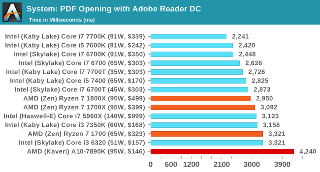
FCAT Processing
One of the more interesting workloads that has crossed our desks in recent quarters is FCAT - the tool we use to measure stuttering in gaming due to dropped or runt frames. The FCAT process requires enabling a color-based overlay onto a game, recording the gameplay, and then parsing the video file through the analysis software. The software is mostly single-threaded, however because the video is basically in a raw format, the file size is large and requires moving a lot of data around. For our test, we take a 90-second clip of the Rise of the Tomb Raider benchmark running on a GTX 980 Ti at 1440p, which comes in around 21 GB, and measure the time it takes to process through the visual analysis tool.
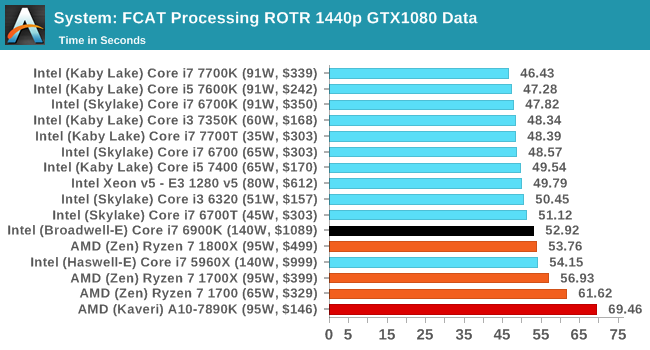
3D Particle Movement v2.1
This is the latest version of the self-penned 3DPM benchmark. The goal of 3DPM is to simulate semi-optimized scientific algorithms taken directly from my doctorate thesis. Version 2.1 improves over 2.0 by passing the main particle structs by reference rather than by value, and decreasing the amount of double->float->double recasts the compiler was adding in. It affords a ~25% speed-up over v2.0, which means new data.
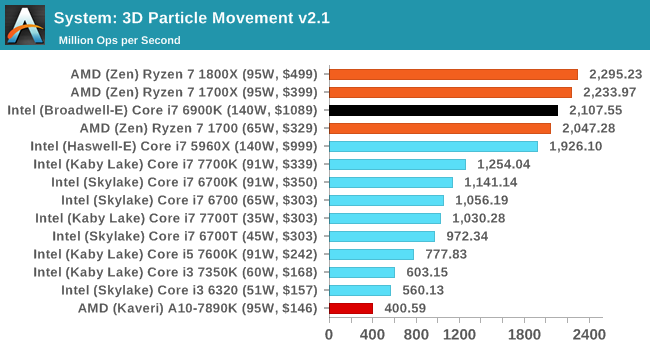
DigiCortex 1.16
Despite being a couple of years old, the DigiCortex software is a pet project for the visualization of neuron and synapse activity in the brain. The software comes with a variety of benchmark modes, and we take the small benchmark which runs a 32k neuron/1.8B synapse simulation. The results on the output are given as a fraction of whether the system can simulate in real-time, so anything above a value of one is suitable for real-time work. The benchmark offers a 'no firing synapse' mode, which in essence detects DRAM and bus speed, however we take the firing mode which adds CPU work with every firing.
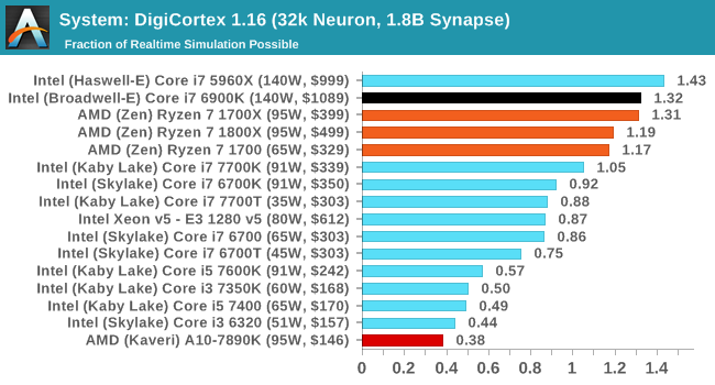
Agisoft Photoscan 1.0
Photoscan stays in our benchmark suite from the previous version, however now we are running on Windows 10 so features such as Speed Shift on the latest processors come into play. The concept of Photoscan is translating many 2D images into a 3D model - so the more detailed the images, and the more you have, the better the model. The algorithm has four stages, some single threaded and some multi-threaded, along with some cache/memory dependency in there as well. For some of the more variable threaded workload, features such as Speed Shift and XFR will be able to take advantage of CPU stalls or downtime, giving sizeable speedups on newer microarchitectures.
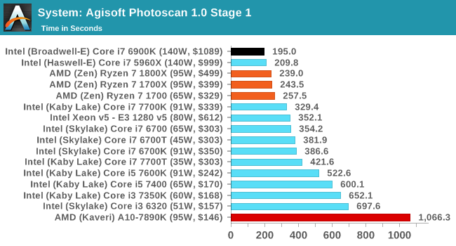
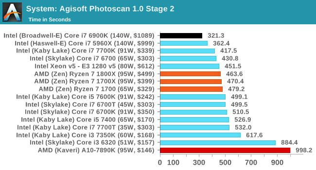
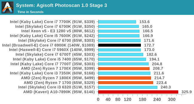
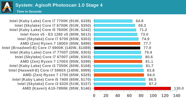
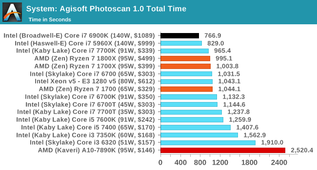
Benchmarking Performance: CPU Rendering Tests
Rendering tests are a long-time favorite of reviewers and benchmarkers, as the code used by rendering packages is usually highly optimized to squeeze every little bit of performance out. Sometimes rendering programs end up being heavily memory dependent as well - when you have that many threads flying about with a ton of data, having low latency memory can be key to everything. Here we take a few of the usual rendering packages under Windows 10, as well as a few new interesting benchmarks.
Corona 1.3
Corona is a standalone package designed to assist software like 3ds Max and Maya with photorealism via ray tracing. It's simple - shoot rays, get pixels. OK, it's more complicated than that, but the benchmark renders a fixed scene six times and offers results in terms of time and rays per second. The official benchmark tables list user submitted results in terms of time, however I feel rays per second is a better metric (in general, scores where higher is better seem to be easier to explain anyway). Corona likes to pile on the threads, so the results end up being very staggered based on thread count.
Blender 2.78
For a render that has been around for what seems like ages, Blender is still a highly popular tool. We managed to wrap up a standard workload into the February 5 nightly build of Blender and measure the time it takes to render the first frame of the scene. Being one of the bigger open source tools out there, it means both AMD and Intel work actively to help improve the codebase, for better or for worse on their own/each other's microarchitecture.
LuxMark
As a synthetic, LuxMark might come across as somewhat arbitrary as a renderer, given that it's mainly used to test GPUs, but it does offer both an OpenCL and a standard C++ mode. In this instance, aside from seeing the comparison in each coding mode for cores and IPC, we also get to see the difference in performance moving from a C++ based code-stack to an OpenCL one with a CPU as the main host.
POV-Ray 3.7
Another regular benchmark in most suites, POV-Ray is another ray-tracer but has been around for many years. It just so happens that during the run up to AMD's Ryzen launch, the code base started to get active again with developers making changes to the code and pushing out updates. Our version and benchmarking started just before that was happening, but given time we will see where the POV-Ray code ends up and adjust in due course.
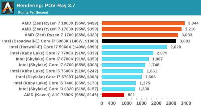
Cinebench R15
The latest version of CineBench has also become one of those 'used everywhere' benchmarks, particularly as an indicator of single thread performance. High IPC and high frequency gives performance in ST, whereas having good scaling and many cores is where the MT test wins out.
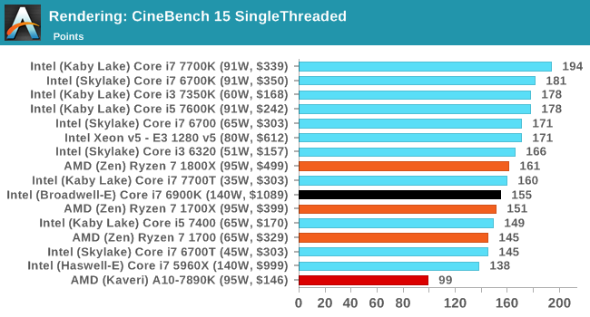
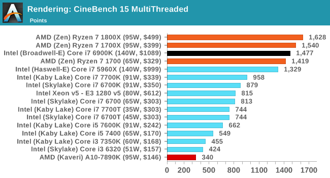
Benchmarking Performance: CPU Web Tests
One of the issues when running web-based tests is the nature of modern browsers to automatically install updates. This means any sustained period of benchmarking will invariably fall foul of the 'it's updated beyond the state of comparison' rule, especially when browsers will update if you give them half a second to think about it. Despite this, we were able to find a series of commands to create an un-updatable version of Chrome 56 for our 2017 test suite. While this means we might not be on the bleeding edge of the latest browser, it makes the scores between CPUs comparable.
SunSpider 1.0.2 [link]
The oldest web-based benchmark in this portion of our test is SunSpider. This is a very basic javascript algorithm tool, and ends up being more a measure of IPC and latency than anything else, with most high performance CPUs scoring around about the same. The basic test is looped 10 times and the average taken. We run the basic test 4 times.
Mozilla Kraken 1.1 [link]
Kraken is another Javascript based benchmark, using the same test harness as SunSpider, but focusing on more stringent real-world use cases and libraries, such as audio processing and image filters. Again, the basic test is looped ten times, and we run the basic test four times.
Google Octane 2.0 [link]
Along with Mozilla, as Google is a major browser developer, having peak JS performance is typically a critical asset when comparing against the other OS developers. In the same way that SunSpider is a very early JS benchmark, and Kraken is a bit newer, Octane aims to be more relevant to real workloads, especially in power constrained devices such as smartphones and tablets.
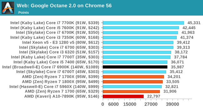
WebXPRT 2013 and 2015 [link]
While the previous three benchmarks do calculations in the background and represent a score, WebXPRT is designed to be a better interpretation of visual workloads that a professional user might have, such as browser based applications, graphing, image editing, sort/analysis, scientific analysis and financial tools. Web2013 is the older tool, superceded by Web2015, however both still are highly relevant for high-performance web applications today.
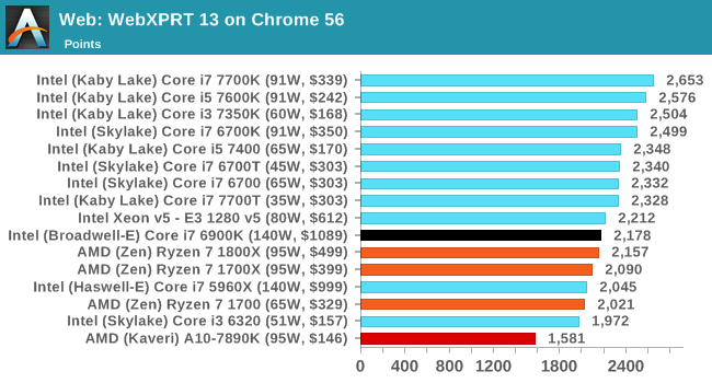
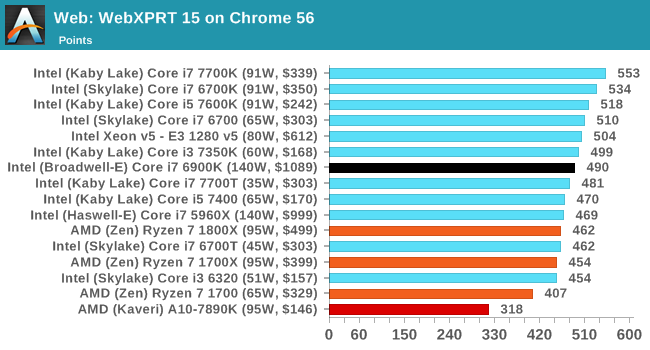
Benchmarking Performance: CPU Encoding Tests
One of the interesting elements on modern processors is encoding performance. This includes encryption/decryption, as well as video transcoding from one video format to another. In the encrypt/decrypt scenario, this remains pertinent to on-the-fly encryption of sensitive data - a process by which more modern devices are leaning to for software security. Video transcoding as a tool to adjust the quality, file size and resolution of a video file has boomed in recent years, such as providing the optimum video for devices before consumption, or for game streamers who are wanting to upload the output from their video camera in real-time. As we move into live 3D video, this task will only get more strenuous, and it turns out that the performance of certain algorithms is a function of the input/output of the content.
7-Zip
One of the freeware compression tools that offers good scaling performance between processors is 7-Zip. It runs under an open-source licence, is fast, and easy to use tool for power users. We run the benchmark mode via the command line for four loops and take the output score.
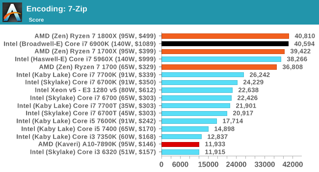
WinRAR 5.40
For the 2017 test suite, we move to the latest version of WinRAR in our compression test. WinRAR in some quarters is more user friendly that 7-Zip, hence its inclusion. Rather than use a benchmark mode as we did with 7-Zip, here we take a set of files representative of a generic stack (33 video files in 1.37 GB, 2834 smaller website files in 370 folders in 150 MB) of compressible and incompressible formats. The results shown are the time taken to encode the file. Due to DRAM caching, we run the test 10 times and take the average of the last five runs when the benchmark is in a steady state.
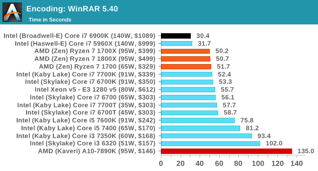
AES Encoding
Algorithms using AES coding have spread far and wide as a ubiquitous tool for encryption. Again, this is another CPU limited test, and modern CPUs have special AES pathways to accelerate their performance. We often see scaling in both frequency and cores with this benchmark. We use the latest version of TrueCrypt and run its benchmark mode over 1GB of in-DRAM data. Results shown are the GB/s average of encryption and decryption.
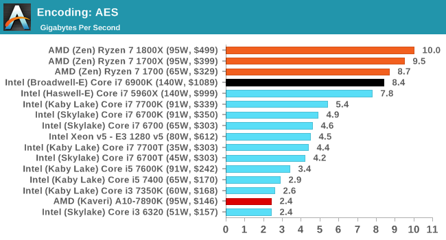
HandBrake H264 and HEVC
As mentioned above, video transcoding (both encode and decode) is a hot topic in performance metrics as more and more content is being created. First consideration is the standard in which the video is encoded, which can be lossless or lossy, trade performance for file-size, trade quality for file-size, or all of the above can increase encoding rates to help accelerate decoding rates. Alongside Google's favorite codec, VP9, there are two others that are taking hold: H264, the older codec, is practically everywhere and is designed to be optimized for 1080p video, and HEVC (or H265) that is aimed to provide the same quality as H264 but at a lower file-size (or better quality for the same size). HEVC is important as 4K is streamed over the air, meaning less bits need to be transferred for the same quality content.
Handbrake is a favored tool for transcoding, and so our test regime takes care of three areas.
Low Quality/Resolution H264: He we transcode a 640x266 H264 rip of a 2 hour film, and change the encoding from Main profile to High profile, using the very-fast preset.
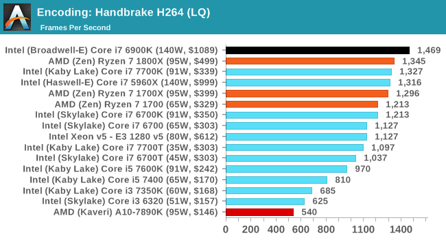
High Quality/Resolution H264: A similar test, but this time we take a ten-minute double 4K (3840x4320) file running at 60 Hz and transcode from Main to High, using the very-fast preset.
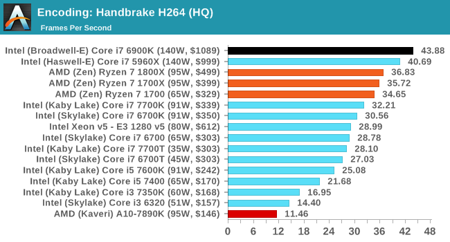
HEVC Test: Using the same video in HQ, we change the resolution and codec of the original video from 4K60 in H264 into 1080p30 HEVC. This causes a dramatic reduction in filesize.
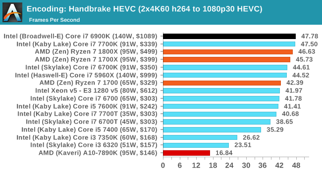
Benchmarking Performance: CPU Office Tests
The office programs we use for benchmarking aren't specific programs per-se, but industry standard tests that hold weight with professionals. The goal of these tests is to use an array of software and techniques that a typical office user might encounter, such as video conferencing, document editing, architectural modelling, and so on and so forth. At present we have two such tools to use.
PCMark8
Despite originally coming out in 2008/2009, Futuremark has maintained PCMark8 to remain relevant in 2017. On the scale of complicated tasks, PCMark focuses more on the low-to-mid range of professional workloads, making it a good indicator for what people consider 'office' work. We run the benchmark from the commandline in 'conventional' mode, meaning C++ over OpenCL, to remove the graphics card from the equation and focus purely on the CPU. PCMark8 offers Home, Work and Creative workloads, with some software tests shared and others unique to each benchmark set. The Creative workload unfortunately seems to fail from the commandline, as the graphical test gives an output of zero (update 3/8: we've found a way around this; will update when we get CPUs retested).
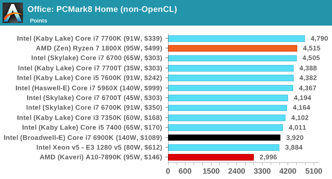
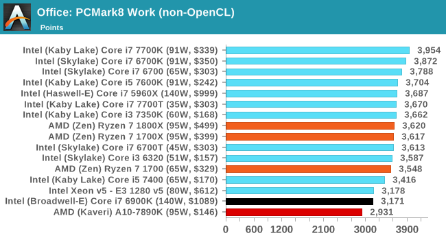
Addendum on 3/8: Originally we posted PCM8 Home scores for Ryzen that were around 3800. On further inspection, these runs were misconfigured due to circumstances beyond our control, and test data is being re-run. The Ryzen 7 1800X in this instance scores 4515.
SYSmark 2014
SYSmark is developed by Bapco, a consortium of industry CPU companies. The goal of SYSmark is to take stripped down versions of popular software, such as Photoshop and Onenote, and measure how long it takes to process certain tasks within that software. The end result is a score for each of the three segments (Office, Media, Data) as well as an overall score. Here a reference system (Core i3-4130, 4GB DRAM, 500GB HDD) is used to provide a baseline score of 1000. A newer version of the benchmark (2014 SE) will be used in future reviews.
A note on contect for these numbers. AMD left Bapco in the last two years, due to differences of opinion on how the benchmarking suites were angled towards Intel processors and had optimizations to show bigger differences than what AMD felt was present. The following benchmarks are provided as data, but the conflict of opinion between the two companies on the validity of the benchmark is provided as context for the following numbers.


Benchmarking Performance: CPU Legacy Tests
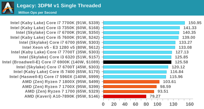
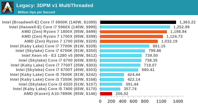
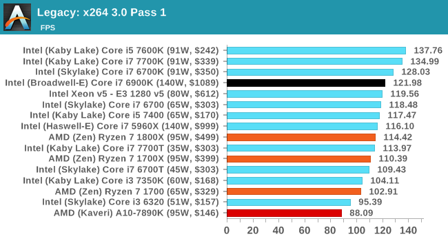
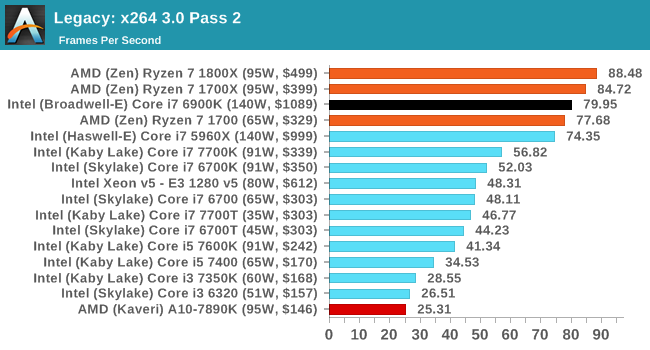
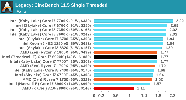
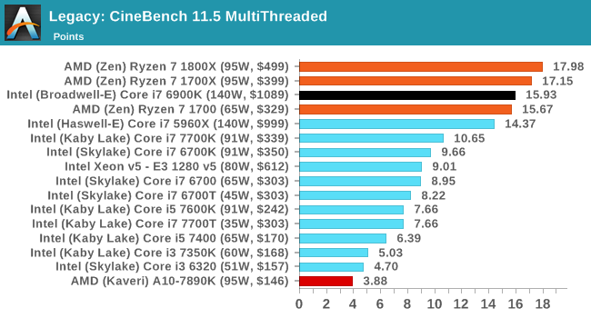
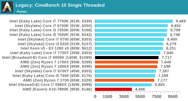
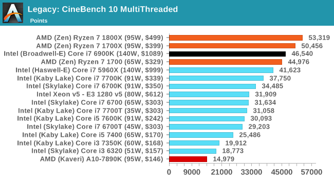
Conclusion
The march towards Ryzen has been a long road for AMD. Anyone creating a new CPU microarchitecture deserves credit as designing such a complex thing requires millions of hours of hard graft. Nonetheless, hard graft doesn’t always guarantee success, and AMD’s targets of low power, small area, and high-performance while using x86 instructions was a spectacularly high bar, especially with a large blue incumbent that regularly outspends them in R&D many times over.
Through the initial disclosures on the Zen microarchitecture, one thing was clear when speaking to the senior staff, such as Dr. Lisa Su, Mark Papermaster, Jim Anderson, Mike Clark, Sam Naffziger and others: that quiet confidence an engineer gets when they know their product is not only good but competitive. The PR campaign up until this point of launch has been managed (we assume) such that the trickle of information comes down the pipe and keeps people on the edge of their seat. Given the interest in Ryzen, it has worked.
Ryzen is AMD’s first foray into CPUs on 14nm, and using FinFETs, as well as a new microarchitecture and pulling in optimization methods from previous products such as Excavator/Carrizo and the GPU line. If we were talking tick-tock strategy, such as Intel’s process over the last decade, this is both a tick and a tock in one. Ryzen is the first part of that strategy, on the desktop processors first, with server parts coming out in Q2 and Notebook APUs in 2H17. One of the main concerns with AMD is typically the ability to execute – get enough good parts out on time and with sufficient performance to merit their launch. As Dr. Su said in our interview, it’s one big hurdle but there are many to come.
| AMD Ryzen 7 SKUs | ||||||
| Cores/ Threads |
Base/ Turbo |
L3 | TDP | Cost | Launch Date | |
| Ryzen 7 1800X | 8/16 | 3.6/4.0 | 16 MB | 95 W | $499 | 3/2/2017 |
| Ryzen 7 1700X | 8/16 | 3.4/3.8 | 16 MB | 95 W | $399 | 3/2/2017 |
| Ryzen 7 1700 | 8/16 | 3.0/3.7 | 16 MB | 65 W | $329 | 3/2/2017 |
Today’s launch of three CPUs, part of the Ryzen 7 family, will be followed by Ryzen 5 in Q2 and Ryzen 3 later in the year. Ryzen 7 uses a single eight-core die, and uses simultaneous multi-threading (SMT) to provide sixteen threads altogether, up to 4.0 GHz on the top Ryzen 7 1800X chip for $499. Officially AMD is positioning the 1800X as a direct competitor to Intel’s i7-6900K, an 8-core processor with hyperthreading that costs over $1000. In our benchmarks, it’s been clear that this battle goes toe-to-toe.
Analyzing the Results
In the brief time we had before getting a sample and this review, we were able to run our new benchmark suite on twelve different Intel CPUs, as well as AMD’s former APU crown holder, the A10-7890K. Throughout the discussion about Ryzen, AMD was advertising a 40%+ gain in raw performance per clock over their previous generations, which was then upped to 52% when the CPUs were actually announced. Back of the envelope calculations put Ryzen at the level of the high-end desktop Broadwell CPUs or just about, which means it would be a case of pure frequency. That being said, Intel is already running CPUs two generations ahead on its mainstream platform, such as the Kaby-Lake based i7-7700K, so it’s going to be an interesting analysis.
Multi-Threaded Tests
First up, AMD’s strength in our testing was clearly in the multithreaded benchmarks. Given the microarchitectures of AMD’s and Intel’s high-performance x86 cores are somewhat similar, for the most part there’s a similar performance window. Intel’s design is slightly wider and has a more integrated cache hierarchy, meaning it manages to win out on ‘edge cases’ that might be a result of bad code. As one might expect, it takes a lot of R&D to cater for particular edge cases.
But as a workstation-based core design, the Zen microarchitecture pulls no punches. As long as the software doesn’t need strenuous AVX code, and manages its memory carefully (such as false sharing), the performance of Ryzen in conventional multi-threaded CPU environments means AMD is back in the game. This is going to be beneficial for the Zen microarchitecture when we see it applied into server environments, especially those that require virtualization.
Single Threaded Tests
Since the launch of Bulldozer, AMD has always been a step behind on single-threaded performance. ST performance is a holy-grail of x86 core design, but often requires significantly advanced features that can potentially burn extra power to get there. AMD’s message on this, even in our interview with Dr. Su, is that AMD has the ability to innovate. This is why AMD promotes features such as SenseMI for their new advanced pre-fetch algorithms, why implementing a micro-op cache into the core was a big thing, and how having double the L2 cache over Intel’s comparable parts were important to the story. Nonetheless, AMD hammered down that a 40%+ IPC gain into its narrative, which then folded into a 52% gain at launch. We’ll take a deeper look into this in a separate review, but our single threaded results show that AMD is back in the fight.
Most of the data points in this graph come from Intel Kaby Lake processors at various frequencies, but the important thing here is that the Ryzen parts are at least in the mix, sitting above the other eight core parts on the far right of the graph. Also, the jump from the A10 up to the 1700 is a big generational jump, let alone considering the 1800X.
Overall Performance
Putting these two elements into the same graph gives the following:
By this measure, for overall performance, it’s clear the Core i7-7700K is still better in price/performance. However, AMD would argue that the competition for the Ryzen 7 parts is on the right, with the i7-6900K and i7-5960X. In our CPU-based results, AMD wins this performance per dollar hands down.
Some Caveats
Since testing this review, and waiting a few days to even write the conclusion, there has been much going on about ways in which AMD’s performance is perhaps being neutered. This list includes discussions around:
- Windows 10 RTC disliking 0.25x multipliers, causing timing issues,
- Software not reading L3 properly (thinking each core has 8MB of L3, rather than 2MB/core),
- Latency within a CCX being regular, but across CCX boundaries having limited bandwidth,
- Static partitioning methods being used shows performance gains when SMT is disabled,
- Ryzen showing performance gains with faster memory, more so than expected,
- Gaming Performance, particularly towards 240 Hz gaming, is being questioned,
- Microsoft’s scheduler not understanding the different CCX core-to-core latencies,
- Windows not scheduling threads within a CCX before moving onto the next CCX,
- Some motherboards having difficulty with DRAM compatibility,
- Performance related EFIs being highly regularly near weekly since two weeks before launch.
A number of these we are already taking steps to measure. Some of the fixes to these issues come from Microsoft’s corner, and we are already told that both AMD and Microsoft are underway to implement scheduling routines to fix these. Other elements will be AMD focused: working with software companies to ensure that after a decade of programming for the other main x86 microarchitecture, it’s a small step to also consider the Zen platform.
At this point, we’re unsure at what level some of these might be default design issues with Zen. The issue of single-thread performance increasing when SMT is disabled (we’ve done some pre-testing, up to 6% in ST) is clearly related to the design of the core, with static partitioning vs competitive partitioning of certain parts of the design. The CCX latency and detection is one that certainly needs further investigation.
The future according to Senior Fellow Mike Clark, one of the principle engineers on the Zen microarchitecture, is that AMD knows where the easy gains are for their next generation product (codenamed Zen 2), and they're already working through the list. A question is then if Intel continues at 5% performance gains clock for clock each year, can AMD make 5-15% and close the gap?
The Silver Lining
It is relevant to point out that Intel is on its 7th Generation of Core microarchitecture. Sure, it looks significantly different when it was designed, but software vendors have had seven generations to optimize for it. Coming in and breaking the incumbent’s stranglehold is difficult, when every software vendor knows that design in and out. While AMD’s design looks similar to Intel, there are nuances which programmers might not have expected, and so it might be a good couple of years before the programming guides have made their way through into production software.
But,
When we look at the CPU benchmarks as part of this review, which have a strong range in algorithm difficulty and dependency, AMD still does well. There’s no getting around that AMD has a strong workstation core design on their hands. This bodes well for users who need compute at a lower cost, especially when you can pick up an eight-core Ryzen 7 at half the cost of the competition.
This makes the server story for AMD, under Naples, much more interesting.
AnandTech Recommended Award
For Performance/Price on a Workstation CPU


