Original Link: https://www.anandtech.com/show/10525/ten-year-anniversary-of-core-2-duo-and-conroe-moores-law-is-dead-long-live-moores-law
Ten Year Anniversary of Core 2 Duo and Conroe: Moore’s Law is Dead, Long Live Moore’s Law
by Ian Cutress on July 27, 2016 10:30 AM EST- Posted in
- CPUs
- Intel
- Core 2 Duo
- Conroe
- ITRS
- Nostalgia
- Time To Upgrade
Today marks a full 10 years since the first Core 2 Duo processors, and hence Intel’s 64-bit Core microarchitecture, were made officially available at retail. These included a number of popular dual-core processor parts, including the seemingly ubiquitous E6400 and the Core 2 Extreme X6800. These were built on Intel’s 65nm process, and marked a turning point in the desktop processor ecosystem. To quote Anand in our launch review: ‘you’re looking at the most impressive piece of silicon the world has ever seen’.
Ten Year Anniversary of Core 2 Duo and Conroe
As part of this piece we will also look at some of the predictions for the future, from the latest (and possibly last) International Technology Roadmap for Semiconductors report, which predicts the stalling of smaller silicon manufacturing nodes over the next 10-15 years.
The first part of this article borrows heavily from Johan’s original look into the Intel Core microarchitecture back in 2006. It’s an awesome read.
Back When I Were A Lad
For a number of our readers, the launch of Conroe was a vast change in the processing landscape. The family of Netburst, Northwood and Prescott processors, in the form of Pentium D and Pentium 4, showed that pursuing the frequency race pushed the silicon far outside its efficiency zone and left a hot, power hungry mess in its wake. It didn’t even come with a muscular V8 sound, and AMD’s Athlon 64 X2 line had taken both the performance and efficiency crown.
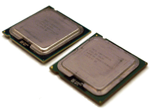
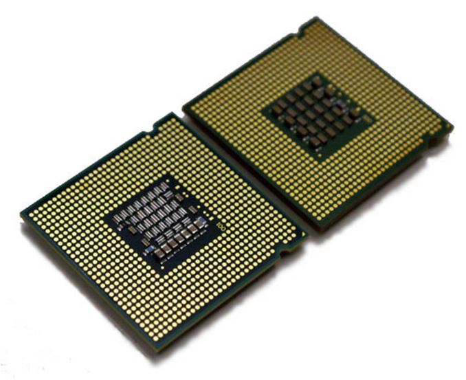
Core 2 Duo (left) vs Pentium D (right)
From the perspective of Intel, it had to incorporate a significant paradigm shift in the way it approached the core microarchitecture – no more long pipelines to bump up clock rates to start. The Core microarchitecture design was marketed as a blend of Pentium Pro and Pentium M techniques, as well as the Netburst architecture, however as Johan pointed out at the time, it is significantly Pentium M and it is very hard to find anything Netburst in there. It wasn’t as simple as ‘adding a few functional units or decoders on Yonah and calling it a day’, almost 80% of the architecture and circuit design had to be redone.
As part of this piece, we’re going to take another look at the original architecture improvements of the Core microarchitecture design and some of our old performance metrics from a decade ago.
27th July 2006: Core 2 Launch Day
Ten years ago, Intel launched the following five processors:
| CPU | Clock Speed | L2 Cache |
| Intel Core 2 Extreme X6800 | 2.93GHz | 4MB |
| Intel Core 2 Duo E6700 | 2.66GHz | 4MB |
| Intel Core 2 Duo E6600 | 2.40GHz | 4MB |
| Intel Core 2 Duo E6400 | 2.13GHz | 2MB |
| Intel Core 2 Duo E6300 | 1.86GHz | 2MB |
The X6800 sits at the top with a higher clock speed with a higher supported FSB-to-core ration than previous Intel processors. The Core 2 processors all came from a 143mm2 die, compared the 162mm2 of Pentium D, and they both seem tiny by comparison to the large die sizes we see 2016 for things like the P100. These were chips without integrated graphics either. The introduction of Core 2 pushed the prices of the Pentium D processors down, to give this interesting table:
| CPU | Clock Speed | L2 Cache | Price |
| Intel Core 2 Extreme X6800 | 2.93GHz | 4MB | $999 |
| Intel Core 2 Duo E6700 | 2.66GHz | 4MB | $530 |
| Intel Core 2 Duo E6600 | 2.40GHz | 4MB | $316 |
| Intel Core 2 Duo E6400 | 2.13GHz | 2MB | $224 |
| Intel Core 2 Duo E6300 | 1.86GHz | 2MB | $183 |
| Intel Pentium D 945 | 3.40GHz | 2MBx2 | $163 |
| Intel Pentium D 915 | 2.80GHz | 2MBx2 | $133 |
| Intel Pentium D 820 | 2.80GHz | 1MBx2 | $113 |
| Intel Pentium D 805 | 2.66GHz | 1MBx2 | $93 |
Comparing this to recent Intel processors, and the X8600 matches the list price of the Core i7-5960X (an 8-core part), whereas the popular Core 2 Duo E6400 at $224 at the same price as the Core i5-6600.
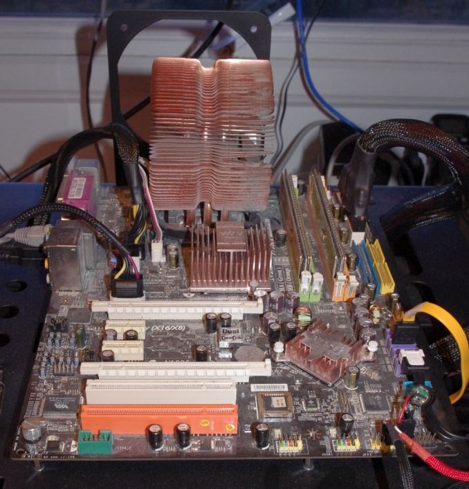
A few years ago, I salvaged a super old computer of mine with an E6400 and took it for a spin for a pipeline piece entitled ‘Dragging Core 2 Duo into 2013’. We know that a number of users today are still using the old platform as their day to day machine, and given that it is now celebrating its 10th birthday, it is interesting that anyone wanting to play around with the old hardware can get a motherboard, memory and CPU from eBay for $50-70.
My crusty C2D Setup from 2013
Core: It’s all in the Prefetch
In a simple CPU design, instructions are decoded in the core and data is fetched from the caches. In a perfect world, such as the Mill architecture, the data and instructions are ready to go in the lowest level cache at all times. This allows for the lowest latency and removes a potential bottleneck. Real life is not that rosy, and it all comes down to how the core can predict what data it needs and has enough time to drag it down to the lowest level of cache it can before it is needed. Ideally it needs to predict the correct data, and not interfere with memory sensitive programs. This is Prefetch.
The Core microarchitecture added multiple prefetchers in the design, as well as improving the prefetch algorithms, to something not seen before on a consumer core. For each core there are two data and one instruction prefetchers, plus another couple for the L2 cache. That’s a total of eight for a dual core CPU, with instructions not to interfere with ‘on-demand’ bandwidth from running software.
One other element to the prefetch is tag lookup for cache indexing. Data prefetchers do this, as well as running software, so in order to avoid a higher latency for the running program, the data prefetch uses the store port to do this. As a general rule (at least at the time), loads happen twice as often as stores, meaning that the store port is generally more ‘free’ to be used for tag lookup by the prefetchers. Stores aren’t critical for most performance metrics, unless the system can’t process stores quickly enough that it backs up the pipeline, but in most cases the rest of the core will be doing things regardless. The cache/memory sub-system is in control for committing the store through the caches, so as long as this happens eventually the process works out.
Core: More Cache Please
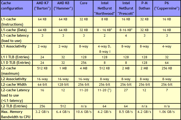
Without having access to a low latency data and instruction store, having a fast core is almost worthless. The most expensive SRAMs sit closest to the execution ports, but are also the smallest due to physical design limitations. As a result, we get a nested cache system where the data you need should be in the lowest level possible, and accesses to higher levels of cache are slightly further away. Any time spent waiting for data to complete a CPU instruction is time lost without an appropriate way of dealing with this, so large fast caches are ideal. The Core design, over the previous Netburst family but also over AMD’s K8 ‘Hammer’ microarchitecture, tried to swat a fly with a Buick.
Core gave a 4 MB Level 2 cache between two cores, with a 12-14 cycle access time. This allows each core to use more than 2MB of L2 if needed, something Presler did not allow. Each core also has a 3-cycle 32KB instruction + 32KB data cache, compared to the super small Netburst, and also supports 256 entries in the L1 data TLB, compared to 8. Both the L1 and L2 are accessible by a 256-bit interface, giving good bandwidth to the core.
Note that AMD’s K8 still has a few advantages over Core. The 2-way 64KB L1 caches on AMD’s K8 have a slightly better hit rate to the 8-way 32KB L1 caches on Core, with a similar latency. AMD’s K8 also used an on-die memory controller, lowering memory latency significantly, despite the faster FSB of Intel Core (relative to Netburst) giving a lower latency to Core. As stated in our microarchitecture overview at the time, Athlon 64 X2s memory advantage had gotten smaller, but a key element to the story is that these advantages were negated by other memory sub-system metrics, such as prefetching. Measured by ScienceMark, the Core microarchitecture’s L1 cache delivers 2x bandwidth, and the L2 cache is about 2.5x faster, than the Athlon one.
Core: Decoding, and Two Goes Into One
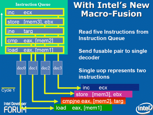
The role of the decoder is to decipher the incoming instruction (opcode, addresses), and translate the 1-15 byte variable length instruction into a fixed-length RISC-like instruction that is easier to schedule and execute: a micro-op. The Core microarchitecture has four decoders – three simple and one complex. The simple decoder can translate instructions into single micro-ops, while the complex decoder can convert one instruction into four micro-ops (and long instructions are handled by a microcode sequencer). It’s worth noting that simple decoders are lower power and have a smaller die area to consider compared to complex decoders. This style of pre-fetch and decode occurs in all modern x86 designs, and by comparison AMD’s K8 design has three complex decoders.
The Core design came with two techniques to assist this part of the core. The first is macro-op fusion. When two common x86 instructions (or macro-ops) can be decoded together, they can be combined to increase throughput, and allows one micro-op to hold two instructions. The grand scheme of this is that four decoders can decode five instructions in one cycle.
According to Intel at the time, for a typical x86 program, 20% of macro-ops can be fused in this way. Now that two instructions are held in one micro-op, further down the pipe this means there is more decode bandwidth for other instructions and less space taken in various buffers and the Out of Order (OoO) queue. Adjusting the pipeline such that 1-in-10 instructions are fused with another instruction should account for an 11% uptick in performance for Core. It’s worth noting that macro-op fusion (and macro-op caches) has become an integral part of Intel’s microarchitecture (and other x86 microarchitectures) as a result.
The second technique is a specific fusion of instructions related to memory addresses rather than registers. An instruction that requires an addition of a register to a memory address, according to RISC rules, would typically require three micro-ops:
| Pseudo-code | Instructions |
| read contents of memory to register2 | MOV EBX, [mem] |
| add register1 to register2 | ADD EBX, EAX |
| store result of register2 back to memory | MOV [mem], EBX |
However, since Banias (after Yonah) and subsequently in Core, the first two of these micro-ops can be fused. This is called micro-op fusion. The pre-decode stage recognizes that these macro-ops can be kept together by using smarter but larger circuitry without lowering the clock frequency. Again, op fusion helps in more ways than one – more throughput, less pressure on buffers, higher efficiency and better performance. Alongside this simple example of memory address addition, micro-op fusion can play heavily in SSE/SSE2 operations as well. This is primarily where Core had an advantage over AMD’s K8.
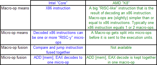
AMD’s definitions of macro-ops and micro-ops differ to that of Intel, which makes it a little confusing when comparing the two:
However, as mentioned above, AMD’s K8 has three complex decoders compared to Core’s 3 simple + 1 complex decoder arrangement. We also mentioned that simple decoders are smaller, use less power, and spit out one Intel micro-op per incoming variable length instruction. AMD K8 decoders on the other hand are dual purpose: it can implement Direct Path decoding, which is kind of like Intel’s simple decoder, or Vector decoding, which is kind of like Intel’s complex decoder. In almost all circumstances, the Direct Path is preferred as it produces fewer ops, and it turns out most instructions go down the Direct Path anyway, including floating point and SSE instructions in K8, resulting in fewer instructions over K7.
While extremely powerful in what they do, AMD’s limitation for K8, compared to Intel’s Core, is two-fold. AMD cannot perform Intel’s version of macro-op fusion, and so where Intel can pack one fused instruction to increase decode throughput such as the load and execute operations in SSE, AMD has to rely on two instructions. The next factor is that by virtue of having more decoders (4 vs 3), Intel can decode more per cycle, which expands with macro-op fusion – where Intel can decode five instructions per cycle, AMD is limited to just three.
As Johan pointed out in the original article, this makes it hard for AMD’s K8 to have had an advantage here. It would require three instructions to be fetched for the complex decoder on Intel, but not kick in the microcode sequencer. Since the most frequent x86 instructions map to one Intel micro-op, this situation is pretty unlikely.
Core: Out of Order and Execution
After Prefetch, Cache and Decode comes Order and Execution. Without rehashing discussions of in-order vs. out-of-order architectures, typically a design with more execution ports and a larger out-of-order reorder buffer/cache can sustain a higher level of instructions per clock as long as the out-of-order buffer is smart, data can continuously be fed, and all the execution ports can be used each cycle. Whether having a super-sized core is actually beneficial to day-to-day operations in 2016 is an interesting point to discuss, during 2006 and the Core era it certainly provided significant benefits.
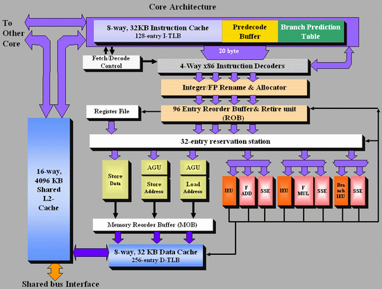
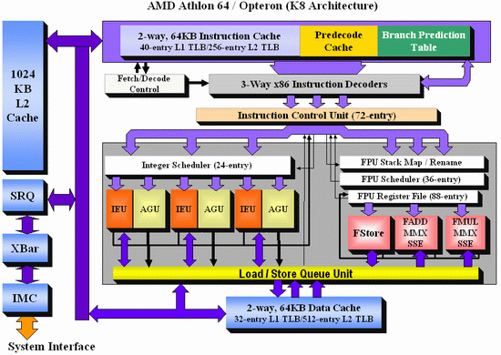
As Johan did back in the original piece, let’s start with semi-equivalent microarchitecture diagrams for Core vs. K8:
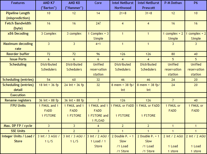
For anyone versed in x86 design, three differences immediately stand out when comparing the two. First is the reorder buffer, which for Intel ranks at 96 entries, compared to 72 for AMD. Second is the scheduler arrangement, where AMD uses split 24-entry INT and 36-entry FP schedulers from the ‘Instruction Control Unit’ whereas Intel has a 32-entry combined ‘reservation station’. Third is the number of SSE ports: Intel has three compared to two from AMD. Let’s go through these in order.
For the reorder buffers, with the right arrangement, bigger is usually better. Make it too big and it uses too much silicon and power however, so there is a fine line to balance between them. Also, the bigger the buffer it is, the less of an impact it has. The goal of the buffer is to push decoded instructions that are ready to work to the front of the queue, and make sure other instructions which are order dependent stay in their required order. By executing independent operations when they are ready, and allowing prefetch to gather data for instructions still waiting in the buffer, this allows latency and bandwidth issues to be hidden. (Large buffers are also key to simultaneous multithreading, which we’ll discuss in a bit as it is not here in Core 2 Duo.) However, when the buffer has the peak number of instructions being sent to the ports every cycle already, having a larger buffer has diminishing returns (the design has to keep adding ports instead, depending on power/silicon budget).
For the scheduler arrangements, using split or unified schedulers for FP and INT has both upsides and downsides. For split schedulers, the main benefit is entry count - in this case AMD can total 60 (24-INT + 36-FP) compared to Intel’s 32. However, a combined scheduler allows for better utilization, as ports are not shared between the split schedulers.
The SSE difference between the two architectures is exacerbated by what we’ve already discussed – macro-op fusion. The Intel Core microarchitecture has 3 SSE units compared to two, but also it allows certain SSE packed instructions to execute within one instruction, due to fusion, rather than two. Two of the Intel’s units are symmetric, with all three sporting 128-bit execution rather than 64-bit on K8. This means that K8 requires two 64-bit instructions whereas Intel can absorb a 128-bit instruction in one go. This means Core can outperform K8 on 128-bit SSE on many different levels, and for 64-bit FP SSE, Core can do 4 DP per cycle, whereas Athlon 64 can do 3.
One other metric not on the diagram comes from branch prediction. Core can sustain one branch prediction per cycle, compared to one per two cycles on previous Intel microarchitectures. This was Intel matching AMD in this case, who already supported one per cycle.
Core: Load Me Up
When discussing the size of the reorder buffer, I mentioned that for some ops relying on the data of others, the order in which they need to be processed has to remain consistent – the load for the second op has to follow the store from the first in order for the calculation to be correct. This works for data that is read from and written to the same location in the same data stream, however with other operations, the memory addresses for loads and stores are not known until they pass the address generation units (AGUs).
This makes reordering a problem at a high level. You ultimately do not want a memory location to be written and stored by two different operations at the same time, or for the same memory address to be used by different ops while one of those ops is sitting in the reorder queue. When a load micro-op enters the buffer, the memory addresses of previous stores are not known until they pass the AGUs. Note, that this applies to memory addresses in the caches as well as main memory. However, if one can speed up loads and load latency in the buffers, this typically has a positive impact in most software scenarios.
With Core, Intel introduced a ‘New Memory Disambiguation’. For lack of a better analogy, this means that the issue of loads preceding stores is given a ‘do it and we’ll clean up after’ approach. Intel stated at the time that the risk that a load will load a value out of an address that is being written to by a store that has yet to be finished is pretty small (1-2%), and the chance decreases with larger caches. So by allowing loads to go head of stores, this allows a speedup but there has to be a catch net for when it goes wrong. To avoid this, a predictor is used to help. The dynamic alias predictor tries to spot this issue. If it happens, the load will have to be repeated, with a penalty of about 20-cycles.
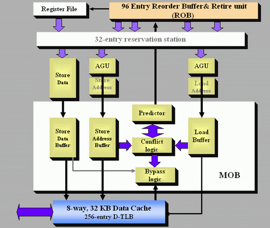
Unofficial AnandTech Diagram
The predictor gives permission for a load to move ahead of a store, and after execution the conflict logic scans the buffer in the Memory reOrder Buffer (MOB) to detect an issue. If it happens, then the load is reprocessed back up the chain. In the worst case scenario, this might reduce performance, but as Johan said back in 2006: ‘realistically it is four steps forward and one step back, resulting in a net performance boost’.
Using this memory disambiguation technique, Intel reported a 40% performance boost purely on allowing loads to be more flexible in a number of synthetic loads (or 10-20% in real world), along with L1 and L2 performance boosts. It is worth noting that this feature affects INT workloads more often than FP workloads, purely on the basis that FP workloads tend to be more ordered by default. This is why AMD’s K8 lost ground to Intel on INT workloads, despite having a lower latency memory system and more INT resources, but stayed on track with FP.
Core: No Hyper-Threading, No Integrated Memory Controller
In 2016, HT and an integrated memory controller (IMC) are now part of the fundamental x86 microarchitecture in the processors we can buy. It can be crazy to think that one of the most fundamental upticks in x86 performance in the last decade lacked these two features. At the time, Intel gave reasons for both.
Simultaneous Hyper-Threading, the act of having two threads funnel data through a single core, requires large buffers to cope with the potential doubling of data and arguably halves resources in the caches, producing more cache pressure. However, Intel gave different reasons at the time – while SMT gave a 40% performance boost, it was only seen as a positive by Intel in server applications. Intel said that SMT makes hotspots even hotter as well, meaning that consumer devices would become power hungry and hot without any reasonable performance improvement.
On the IMC, Intel stated at the time that they had two options: an IMC, or a larger L2 cache. Which one would be better is a matter for debate, but Intel in the end went with a 4 MB L2 cache. Such a cache uses less power than an IMC, and leaving the IMC on the chipset allows for a wider support range of memory types (in this case DDR2 for consumers and FB-DIMM for servers). However, having an IMC on die improves memory latency significantly, and Intel stated that techniques such as memory disambiguation and improved prefetch logic can soak up this disparity.
As we know know, on-die IMCs are the big thing.
Core: Performance vs. Today
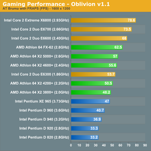
Looking back at Anand’s original review, and at a time where CPU performance made a lot of difference for gaming frame rates at 1600x1200, the conclusion was quite startling.
Intel's Core 2 Extreme X6800 didn't lose a single benchmark in our comparison; not a single one. In many cases, the $183 Core 2 Duo E6300 actually outperformed Intel's previous champ: the Pentium Extreme Edition 965. In one day, Intel has made its entire Pentium D lineup of processors obsolete.
Imagine something like that happening today. (Actually, if you believe what we’ve been told, AMD’s upcoming AM4 platform with Zen and Bristol Ridge might make its current desktop platform obsolete, but that’s a slightly different discussion because of how integrated graphics has adjusted the landscape for CPU focused silicon somewhat.)
That’s Intel vs. Intel though, against AMD it was just as damning.
Compared to AMD's Athlon 64 X2 the situation gets a lot more competitive, but AMD still doesn't stand a chance. The Core 2 Extreme X6800, Core 2 Duo E6700 and E6600 were pretty consistently in the top 3 or 4 spots in each benchmark, with the E6600 offering better performance than AMD's FX-62 flagship in the vast majority of benchmarks.
However, Core 2 Duo has now been out for 10 years. I’ve pulled up some benchmark data from our database to see if we have any matches to compare against processors that cost $214 today. The Core i5-6600 fits our bill perfectly, and there are two benchmarks which match up. I’ve also dotted the graphs with a range of more recent AMD and Intel processors for progression.
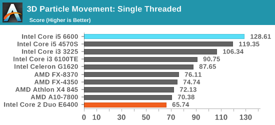
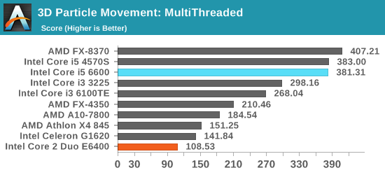
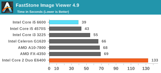
Our 3D Particle Movement is more for idealized synthetic workloads, however FastStone is all about image conversion and favors high frequency, high single threaded performance.
Naturally, modern processors nearing 4.00 GHz have a large advantage over the 2.13 GHz version of Core 2 Duo, as well as multiple generations of improved microarchitecture designs and smaller lithography nodes for power efficiency. However, has any processor family had as much nostalgic longevity as the consumer launch of Core? One could argue that while Core put Intel on top of the heap again, Sandy Bridge was a more important shift in design and as a result, many users went from Conroe to Sandy Bridge and have stayed there.
Looking to the Future:
International Technology Roadmap for Semiconductors 2.0
The ten year anniversary of Conroe comes at a time when the International Technology Roadmap for Semiconductors report into the next 10-15 years of the industry has been officially launched to the public. This biennial report is compiled by a group of experts in the semiconductor industry from the US, Europe and Asia and is designed to help the industry dictate which path to focus R&D for the next 10-15 years, and runs for nearly 500 pages. While we could go into extensive detail about the contents, we plan to give a brief overview here. But for people interested in the industry, it’s a great read for sure.
The report includes deep discussions regarding test equipment, process integration, radio frequency implementations (RF), microelectromechanical systems (MEMs), photolithography, factory integration, assembly, packaging, environmental issues, improving yields, modeling/simulation and emerging materials. With a focused path to a number of technologies, the hope is that leading contenders in each part of the industry can optimize and improve efficiency in directional research and development, with the possibility of collaboration, rather than taking many different routes.
Obviously such a report is going to make successful and unsuccessful predictions, even with a group of experts, based on the introduction of moonshot style features (FinFET) or unforeseen limitations in future development. For example, here is the first roadmap published by the Semiconductor Industry Association in the first report in 1993:
Original 1993 Semiconductor Industry Association roadmap
As we can see, by 2007 it was predicted that we would be on 10nm 100nm chips with up to 20 million ‘gates’, up to 4GB of SRAM per chip and 1250mm2 of logic per die. Up to 400mm wafers were expected in this timeframe, with 200W per die and 0.002 defects per square cm (or 5.65 errors per 300mm wafer).
Compare that to 2016, where we have 16/14nm lithography nodes running 300mm wafers producing 15 billion transistors on a 610mm2 die (NVIDIA P100). Cache currently goes up to 60-65MB on the largest chips, and the power consumption of these chips (the ASIC power) is around 250W as well. So while the predictions were a slow on the lithography node, various predictions about the integration of components onto a base processor were missed (memory controllers, chipsets, other IO).
What makes the most recent report different is that it is listed as the last report planned by ITRS, to be replaced by a more generalized roadmap for devices and systems, the IRDS as the utility of semiconductors has changed over the last decade. In this last report, a number of predictions and focal points have been picked up by the media, indicating a true end to Moore’s Law and how to progress beyond merely shrinking lithography nodes beyond 7nm. Part of this comes from the changing landscape, the move to IoT and the demand for big data processing and storage, but also the decrease in the profitability/performance gain of decreasing node sizes in comparison to their cost to develop is, if believed, set to put a paradigm shift in integrated circuit development. This applies to processors, to mobile, to DRAM and other industry focal points, such as data centers and communications.
I do want to quote one part of the paper verbatim here, as it ties into the fundamental principles of the future of semiconductor engineering:
“Moore’s Law is dead, long live Moore’s Law”
The question of how long will Moore’s Law last has been posed an infinite number of times since the 80s and every 5-10 years publications claiming the end of Moore’s Law have appeared from the most unthinkable and yet “reputedly qualified” sources. Despite these alarmist publications the trend predicted by Moore’s Law has continued unabated for the past 50 years by morphing from one scaling method to another, where one method ended the next one took over. This concept has completely eluded the comprehension of casual observes that have mistakenly interpreted the end of one scaling method as the end of Moore’s Law. As stated before, bipolar transistors were replaced by PMOS that were replaced by NMOS that were also replaced by CMOS. Equivalent scaling succeeded Geometrical Scaling when this could not longer operate and now 3D Power Scaling is taking off.
By 2020-25 device features will be reduces to a few nanometers and it will become practically impossible to reduce device dimensions any further. At first sight this consideration seems to prelude to the unavoidable end of the integrated circuit era but once again the creativity of scientists and engineers has devised a method ‘To snatch victory from the jaws of defeat’.
Looking To The Future: 450mm Wafers in 2021, and Down to ‘2nm’
Most users following the industry will know that the name of the lithographic node, such as ‘14nm’, ‘16nm’ or ‘28nm’ is often an imperfect characterization of what is actually happening on the silicon. For example, Intel’s 14nm node is widely touted as the best in the industry, and the equivalent 14nm/16nm nodes are said to not be even close, due to Intel’s focus on several generations of FinFET compared to the other main semiconductor manufacturers. This also means that while ‘14nm’ or ‘16nm’ is mentioned, many other parts of the silicon could be manufactured on other nodes, depending on the utility.
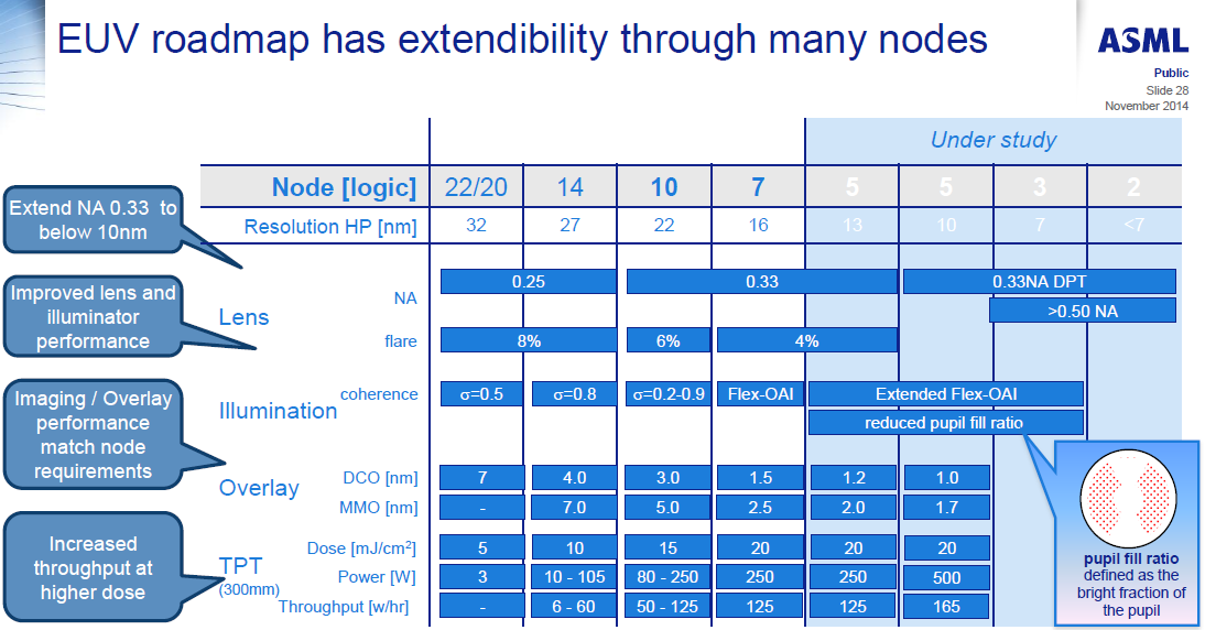
We’ve spoken in the past about equipment roadmaps to deal with the problem of shrinking lithography node sizes. This includes new lasers, droplet generation, collectors, masks, defect detection, lenses, and the technology to drive high throughput. For example, here are ASML’s EUV requirements for the next few manufacturing nodes, including requirements for 250W light sources at a 5nm node:
With the ITRS report, it makes a couple of metrics regarding node sizes and wafers. On the later, we get the prediction that 450mm wafers should be in play at around 2021 for DRAM:
This matches at DRAM half-pitch of 15nm, or a DRAM cell size of 780nm2, compared to 3480nm2 today. The movement to 450mm wafers has been expected for some time, with early predictions going for the 2008-2011 timeframe, however development seems to have stalled for a variety of reasons.
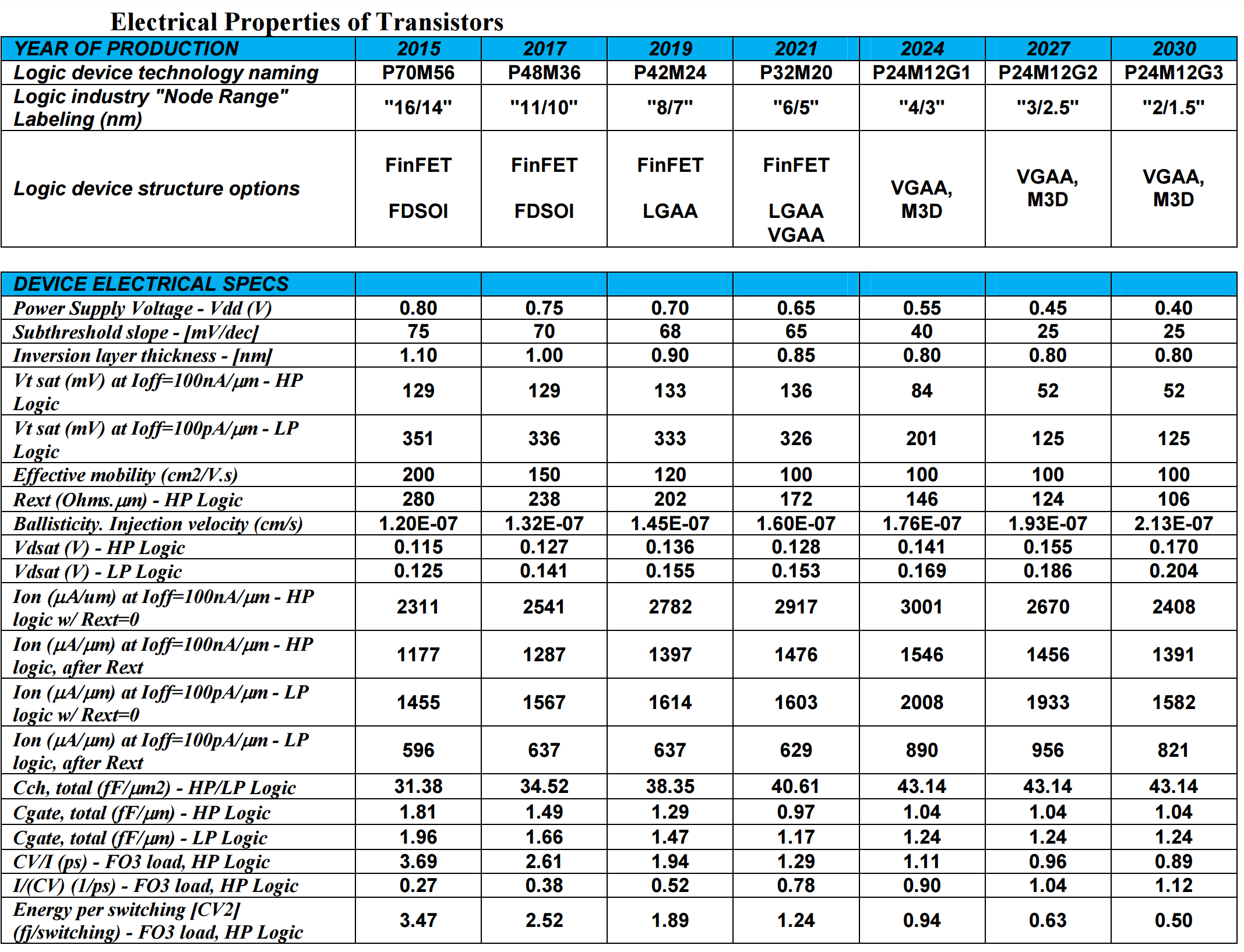
When it comes to transistors, given the node naming scheme caveats listed above, the ITRS report predicts that FinFET will make way at around the 2021 timeframe in favor of 3D stacking such as ‘vertical gate all-around’ (VGAA). As the node shrinks, as well as the transistor size, the power supply voltage will drop from 800mV today down to 400/450mV by 2027.
Moving into a world of IoT will require even lower power transistors, of which moving to a ‘smaller node’ and vertical chip integration will be a large part.
The ITRS report goes into a lot of detail regarding different stacking technologies, such as the 2.5D integration we see on products like AMD’s Fiji GPU involving a silicon interposer, as well as 3D and the different ways to implement both microchannel cooling in such chips as well as 3D TSV applications.
Looking To The Future: NAND Flash Scales Up to 64 TB SSDs in 2030
Over the past few years, the NAND Flash industry has gone through two major shifts in technology: the movement from 1 to 2 to 3 bits per cell, which directly increases bit density and capacity, and also moving from planar flash to variants of 3D stacking. Stacking can refer to individual NAND dies, as well as stacking those dies into a single package: both of these features are being extensively investigated to increase density also. There are two main drivers for this: reduction in cost, and capacity. However, despite this, the predictions in the ITRS report for NAND flash are primarily looking at improvements to numbers of layers rather than lithography changes or moving to more bits per cell.
As we can see, TLC (according to the report) is here to stay. QLC, or whatever you want to call it, is not mentioned. The two changes are the number of memory layers, moving from 32 today to 128 around 2022 and then 256/512 by 2030, and the number of word-lines in one 3D NAND string. This gives a product density projection of 256 Gbit packages today to 1 Tbit packages in 2022 and 4 Tbit packages in 2030.
If we apply this to consumer drives available today, we can extrapolate potential SSD sizes for the future. The current Samsung 850 EVO 4 TB uses Samsung’s 48-layer third generation V-NAND to provide 256 Gbit TLC parts. Alongside the 4 TB of memory, the controller requires 4 GB of DRAM, which is another concern to remember. So despite the report stating 256 Gbit in 32-layer, we have 256 Gbit in 48-layer, which is a difference primarily in die-size predictions for the report. Still, if we go off of the product density we should see 12 TB SSDs by 2020, 16 TB in 2022, 48 TB in 2028 and 64 TB drives in 2030. It’s worth noting that the ITRS report doesn’t mention power consumption in this table, nor controller developments which may be a substantial source of performance and/or capacity implementations.
Looking To The Future: Mobile, 32-cores and 8K Displays
The volume of the mobile industry today is certainly a hot topic, especially with Intel scrapping their mobile platform as recently as April 2016. This primarily leaves ARM (who was recently acquired by Softbank) in the driving seat for providing the next decade of mobile processor designs. Because ARM sells licences, both processor licences and architecture licences, a number of ARM’s partners have taken the base instructions and decided to forgo ARM’s core designs for their own. This is why we currently see Samsung with their M1 core, Qualcomm with their Kryo core, and Apple with their Twister cores as well, while Huawei, Mediatek and others are combining parts of ARM’s core designs with various GPU designs either from ARM or Imagination. Getting the right combination of parts, as well as the industrial design, are key elements to the user experience as well as the mobile industry as a whole.
Then of course, Mediatek announced the Helio X20 last year, which is finally now in devices. This is a 10-core part, using a paradigm such that the most relevant cores needed for performance and power consumption are in play at the right time. The creation of a 10-core part made a number of industry analysts wonder which direction this market was going in, as on the one end we have the Helio X20, while Apple’s latest iPhone family were using dual-core designs of Apple’s custom implementation. So if 10-cores are too much, this roadmap might come a little surprising.
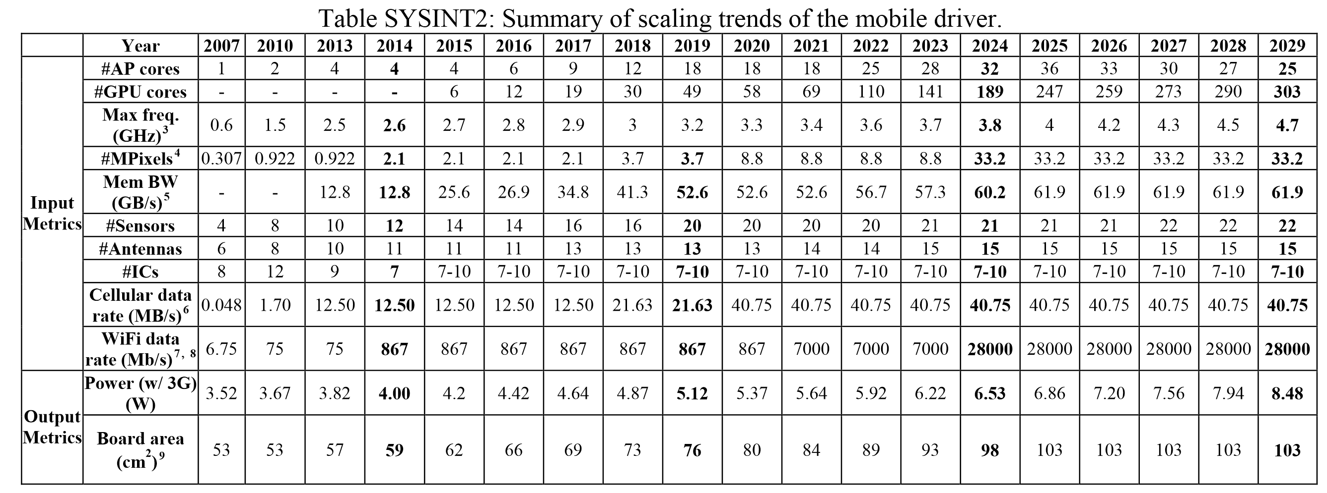
As we stand in 2016, this roadmap states we are currently in a 6-core mobile CPU arrangement with 12 GPU cores, with the CPU running at 2.8 GHz. Displays are around the Full-HD mark, with overall board power at 4.42W. Well we certainly have hex-core parts today (2xA57 + 4xA53), 12-core GPUs also exist in Apple’s products, and Samsung’s M1 core is rated at 2.8 GHz. Some phones, such as Sony’s Xperia Z5 Premium, already have 4K screens (8.3MP), which is more geared towards 2020 in this roadmap.
Cycle now from 2016 to 2025, almost 10 years in the future. ITRS’ roadmap states the following:
- 36-cores
- 247 GPU cores
- 4.0 GHz
- 8K Screens (33.2 MP)
- 61.9 GB/s memory bandwidth
- 28 Gbit/s WiFi
- 6.86W Board Power
- 103 cm2 board area
Now clearly, for this piece I conferred with our mobile team and I got a lot of confused faces. Even scaling down from 16nm in 2016 to 4nm in 2025, they felt that so many all-purpose cores in a chip (as well as all the GPU cores) was probably excessive, not only in terms of utility but also for 2D floor plan. In order to implement this, more z-height would be needed as well as appropriate 3D technologies in place. Andrei felt the frequency targets were more respectable, and the memory bandwidth would depend on how the silicon designers decided to implement on-package DRAM vs multi-channel implementations. The board power seemed a little excessive, if only because the laws of physics can’t change that drastically, and an increase in +50% board area just means a bigger device.
Looking To The Future
While today is Conroe’s 10 year anniversary, I was a post-teenage system builder when it was first released. Now, as AnandTech’s CPU editor, it has been fun for me to delve back into the past and revisit some of the fundamental design changes that would steer a significant amount of Intel’s future design. You can certainly feel many of the technologies used in the Core microarchitecture in Skylake today, including operation fusion and large shared caching. Now of course, a number of technologies have been developed since which make a big difference too, such as micro-op caches from Sandy Bridge, an L3 cache, even adaptations for eDRAM and moving the memory controller and north bridge on-die. But it does make me wonder if there will be another Intel microarchitecture as important as this down the line. On the AMD side of the fence, everyone is looking at Zen with wide eyes and anticipation. While we have been told not to expect it to take the performance crown, a number of users and industry analysts hope that it brings more competition to the x86 space, enough to rekindle the competitive spirit in silicon back in the mid-2000s.
Looking into the International Technology Roadmap for Semiconductors report, and even just the 50-page summary, there are a large number of predictions in the industry that could happen. There are thousands of people working to make sure the next process node, and the one after that, happens with good yields and on time. The report goes into detail about how shrinking that process won’t happen forever, which is a sentiment that the industry has had for a while, and it lays out in a series of working groups what needs to happen at each stage of the process to go beyond Moore’s Law, specifically regarding silicon stacking, TSVs, and the movement to 3D chips. The ITRS report is set to be the last, with the new focus on devices, systems, SiP and other technologies beyond Moore’s Law. Some have heralded the lack of a future ITRS report as a stark warning, however the fact that we can’t keep shrinking forever has been a known fact, especially at the point where most businesses won’t shrink a process node unless it can net them an overall profit. The movement to 3D makes everything a lot more complicated, but it has to happen in order to provide semiconductor growth and improvements beyond 2D.
Sources
Johan’s Conroe vs K8 Architecture Deep Dive, 2006
Anand’s Core 2 Extreme and Core 2 Duo Review, 2006
International Technology Roadmap for Semiconductors 2.0 Report, 2015/2016
Addendum: This article originally stated that the Core 2 Duo/Conroe was derived in part from the Pentium Pro. This was due to typo in the original 2006 article and has since been adjusted.

