Original Link: https://www.anandtech.com/show/10375/arm-unveils-bifrost-and-mali-g71
ARM Unveils Next Generation Bifrost GPU Architecture & Mali-G71: The New High-End Mali
by Ryan Smith on May 30, 2016 7:00 AM EST
Over the last few years the SoC GPU space has taken an interesting path, and one I admittedly wasn’t expecting. At the start of this decade the playing field for SoC-class GPUs was rather diverse, with everyone from NVIDIA to Broadcom (and everything in between) participating in it. Consolidation in the GPU space would be inevitable – something we’ve already seen with SoC vendors dropping out – however I am surprised by just how quickly it has happened. In just six years, the number of GPU vendors with a major presence in high-end Android phones has been whittled down to only two: the vertically integrated Qualcomm, and the IP-licensing ARM.
That ARM has managed to secure most of the licensed GPU market for themselves is a testament to both their engineering and their IP licensing efforts. ARM’s path into this market has been non-traditional, having acquired an essentially unknown GPU vendor a decade ago, and growing it into the 800lb gorilla it has now become. ARM’s expertise in IP licensing, coupled with a somewhat unusual GPU architecture, has proven to be a powerful combination for the company as they have secured a number of significant wins from the high end to the low end.
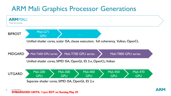
Much of this growth was built on the back of the company’s GPU architecture of the last few years, Midgard. Initially launched in 2012, Midgard has been the cornerstone of ARM’s Mali 600, 700, and 800 series designs. As ARM’s first unified shader design for GPUs, Midgard has been extended over the years to support newer features such as geometry tessellation and 10bpc color, along with newer APIs such as OpenGL ES 3.1/3.2 and Vulkan.
However as Midgard approaches its fourth birthday and the SoC GPU landscape evolves, Midgard’s time at the top will soon be coming to an end. Amidst the backdrop of Computex 2016 and alongside their new Cortex-A73 CPU, ARM is announcing their next generation GPU architecture, Bifrost. A significant update to ARM’s GPU architecture, Bifrost will first be deployed in ARM’s Mali-G71 GPU.
Recap: Mali & VLIW
One of the interesting aspects of SoC GPU development over the years is that it has been a very distinct echo of larger discrete GPU development. Many innovations and changes that first show up with dGPUs will show up in SoC GPUs a few years later, as newer manufacturing processes allow for those developments to fit within the extreme space and power requirements of an SoC-class GPU. At the same time mobile games/graphics development follows a similar path, with mobile application developers picking up rendering techniques first used elsewhere.
ARM’s architectural development, in turn, has been a good example of this process. The non-unified Utgard architecture gave way to the unified Midgard architecture in 2012, about 6 years after dGPUs first made the transition. And as we learned when we examined the Midgard architecture in depth, Midgard was an architecture well suited for the rendering paradigms of the time.
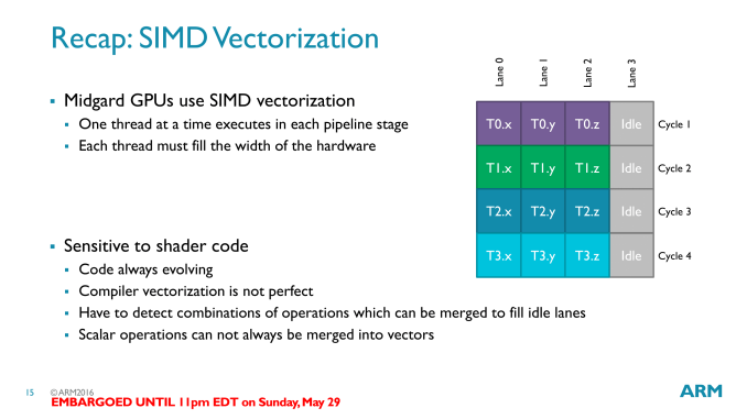
Midgard’s shader core, in short, was an Instruction Level Parallelism-centric design, employing a Very Long Instruction Word (VLIW) instruction format. To achieve maximum utilization out of Midgard’s shader cores, you needed to be able to extract a significant amount of ILP – 4 concurrent instructions – in order to fill all of the slots in a shader core. This sort of design maps well to basic graphics workloads, as 4 color component RGBA is a natural fit for the 4 lanes of ARM’s VLIW-4 design. Furthermore VLIW designs are traditionally very space efficient, as there’s relatively little overhead logic, which is always a boon for the tight constraints of the SoC space.
However getting back to what we said earlier about SoC GPUs being an echo of discrete GPUs, as we’ve seen there, VLIW does have a limited shelf life. Newer rendering paradigms often work with just 1 or 2 components at once, which leaves open lanes that need to be filled to achieve full GPU utilization. A good shader compiler can help here, but it does become an escalating technology war over time, as getting good performance becomes increasingly compiler-centric, and writing a compiler that can extract the necessary ILP is a challenge in and of itself. What history has shown us – and what is going to happen again in the mobile market – is that rendering workloads will continue to shift away from a style that is suitable for VLIW.
The Bifrost Quad: Replacing ILP with TLP
The solution then, as the echo of GPU development catches up with mobile, is to make the move to a scalar, Thread Level Parallelism-centric architecture. And this is exactly the direction ARM is going with Bifrost.
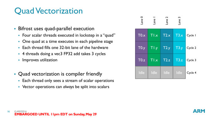
Continuing ARM’s theme of Norse-named architectures, Bifrost is a distinctly TLP-centric (though not TLP-exclusive) architecture. In designing Bifrost, ARM’s GPU group likes to joke that they just turned their old shader core 90° to the left, which all things considered is not a bad analogy. Rather than trying to extract 4 instruction’s worth of ILP from a single thread, ARM groups 4 threads together and executes a single instruction from each one.
If all of this sounds familiar to our long-time readers, then it should. This is a very similar transition to what AMD made with Graphics Core Next in 2011, a move that significantly improved AMD’s GPU throughput and suitability for modern rendering paradigms. And for ARM we are going to see a lot of the same.
The simply beauty of a TLP-centric design is that it doesn’t require making extensive efforts to extract instruction level parallelism from a thread. Graphics rendering itself is an embarrassingly parallel problem, and the increase in screen resolutions over the years has further increased the number of pixels (and therefore threads) that need processed. Thus by nearly eliminating a reliance on ILP, ARM is able to much more easily achieve full utilization of its shader core.
The benefit for ARM here is twofold. In the case of graphics, a TLP-centric design improves utilization, especially with newer rendering paradigms that only operate on one or two components at a time. However increasingly important is the fact that TLP designs are also much more compute friendly, and this is an important distinction for ARM as solid GPU compute performance becomes an increasingly component of modern mobile devices.
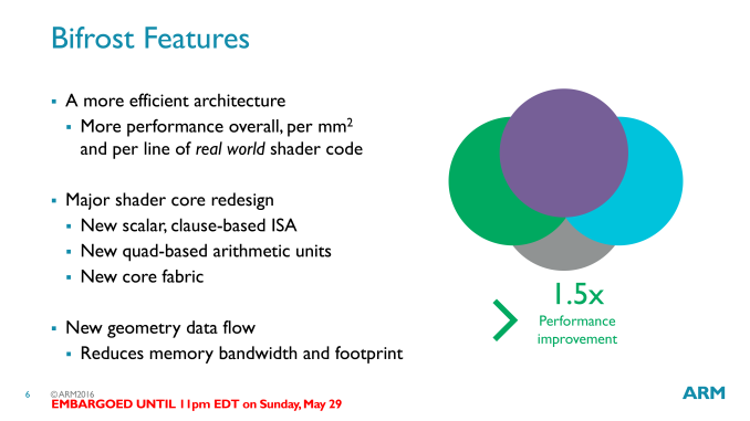
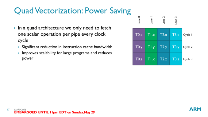
This increase in utilization also has an impact on power consumption, and ultimately area efficiency. In conjunction with architectural improvements made elsewhere, Bifrost’s higher average utilization means the design should have better performance per mm2 of die space, which is an important metric for the market ARM serves. The company’s architectural update also brings with it certain side benefits to aspects such as bandwidth needs for the L1 instruction cache, which allows for a lower power data path between the cache and shader core.
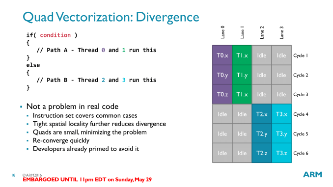
Moving on, within the Bifrost architecture, ARM’s wavefronts are called Quads. True to the name, these are natively 4 threads wide, and a row of instructions from a full quad is executed per clock cycle. Bifrost’s wavefront size is particularly interesting here, as quads are much smaller than competing architectures, which are typically in the 16-32 thread range. Wavefront design in general reflects the need to find a balance between resource/area density and performance. Wide wavefronts require less control logic (ex: 32 threads with 1 unit of control logic, versus 4x8 threads with 8 units of control logic), but at the same time the wider the wavefront, the harder it is to fill.
ARM’s GPU philosophy in general has been concerned with trying to avoid execution stalls, and their choice in wavefront size reflects this. By going with a narrower wavefront, a group of threads is less likely to diverge – that is, take different paths, typically as a result of a conditional statement – than a wider wavefront. Divergences are easy enough to handle (just follow both paths), but the split hurts performance.
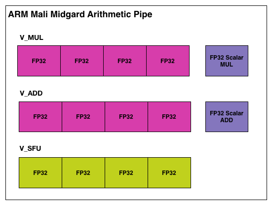
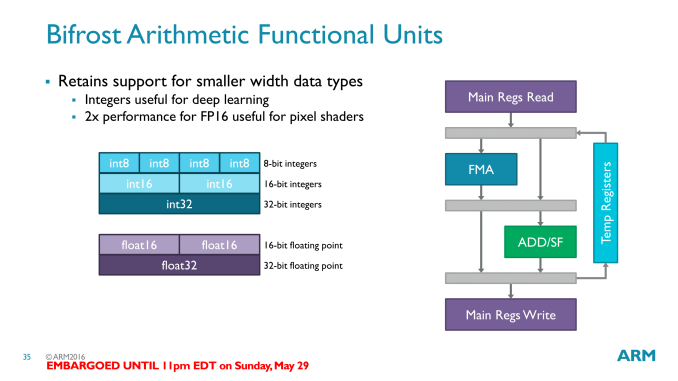
Diving a bit deeper, let’s take a look at the individual arithmetic pipelines inside of a quad execution engine. In Midgard, ARM’s pipelines contained vector units for vector addition, vector multiplication, vector Special Functions Unit (SFU) scalar addition, and scalar multiplication. Bifrost on the other hand simplifies this. With Bifrost a pipeline is just a 128bit (4x32bit) FMA SIMD, and then a second 128bit SIMD for interger addition and SFU operations. Each 32bit slot is in turn filled with an instruction from its respective thread in the quad.
That interger additions and special functions are together on the same SIMD (FP adds are done on the FMA unit) is a unique hallmark of Bifrost, as most other architectures put all addition and multiplication down the same pipe. On the other hand it means that, just like Midgard, ARM can execute a multiplication/FMA and a separate add at the same time. This is also why Bifrost is not a TLP-exclusive design. Technically ARM is issuing a fused instruction, the Slightly Long Instruction Word, which is composed of separate instructions for the FMA and ADD/SFU SIMDs. Consequently to get maximum utilization of the GPU, both SIMDs need to be filled. However with that said, the traditional definitions usually involve just FMAs, so how much this is really reliant on ILP compared to other architectures is up to debate.
Meanwhile within the SIMDs, ARM has confirmed that like with Midgard, Bifrost is capable of instruction decomposition/fusion, meaning that a single SIMD lane can be packed with different data types. For floating point operations one lane can handle 1 FP32 or 2 FP16 per clock, and for integer operations this is 1 INT32, 2 INT16s, or 4 INT8s per clock. This continues to be a differentiating feature of ARM’s GPU architectures as compared to some other designs, as they maintain the single ALU whereas some other vendors use dedicated FP32 and FP16 ALUs, trading between space and power efficiency.
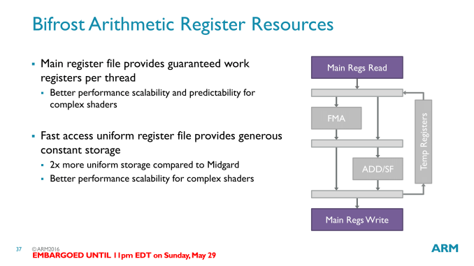
ARM has also confirmed that the register file within each pipeline has been enlarged relative to Midgard. Though a specific size wasn’t specified, Bifrost’s register file size is twice that of Midgard’s. ARM specifically cites this as being important for improving the architecture’s ability to handle long, complex shaders that may have overflowed the register file on Midgard.
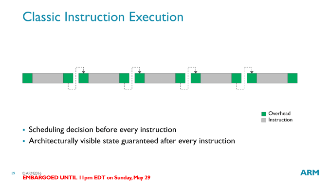
Going back up a level, before getting into a high level overview of Bifrost, let’s talk a bit about how ARM is actually scheduling threads for Bifrost. Along with the reorganization of their shader core into the quad, ARM has also added support for an interesting feature called clauses. Clauses, in a nutshell, are a type of wavefront with restrictions. The idea behind a clause being that by defining additional requirements about how instructions are ordered, and identifying instructions with variable latency, ARM can cut down on instruction scheduling overhead.
When a wavefront is organized into a clause by the compiler, the instructions within that wavefront are given certain execution guarantees. The latency for all instructions is known and they are executed back to back to the end of the clause. In essence a clause is a block of instructions the compiler knows is absolutely safe to run from start to finish without checking in on it.
The payoff for using clauses is that because clauses have execution guarantees, the GPU scheduler can avoid the overhead of checking on a quad execution engine as frequently, only returning to check on it after the clause is done. This overhead reduction then is captured as power savings.
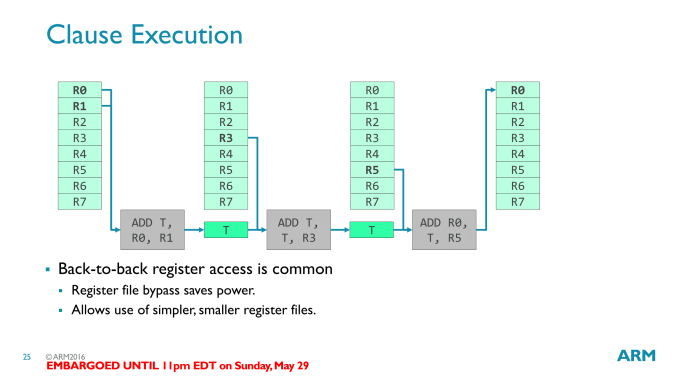
But the benefits to Bifrost from clauses don’t stop there. When executing clauses, Bifrost can chain together instructions that would need to access the same register back-to-back, and in some cases bypass that register access. Register file accesses are relatively expensive from a power standpoint, so avoiding using the register file is another means to save power, and ultimately it allows ARM to get away with a simpler register file.
ARM calls this implementation a temporary register, and while it’s more of a mental mnemonic than a true register, the basic idea is that the result of an instruction is immediately fed into the input of the next instruction. The nature of this data feeding means that it can only take place within a clause, as the result will only be available for a single cycle. This in turn is why the temporary register really is temporary; the data has to be used next cycle or it would be lost.
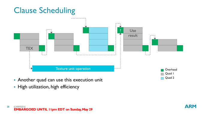
Finally, ARM has also illustrated how clauses work with respect to variable latency instructions, such as texture accesses. Variable latency operations are allowed in a clause, but only at the boundaries of a clause. In essence a variable latency operation splits a clause into two parts, with the access marking the end of a clause and the operation using the resource accessed marking the start of another clause.
By splitting clauses in this manner, ARM is able to schedule clauses around these variable latency operations. When the second half of a clause is not ready to begin, another, unrelated clause can be interleaved into the quad. Interleaving clauses is a textbook solution to latency hiding, as it allows the quads to stay active with other work while waiting on high latency operations, with each clause/wavefront covering for the latency of the others. In the case of ARM, Bifrost just takes it one step further due to the introduction of clauses, more strictly defining when interleaving takes place. Overall ARM can interleave up to 8 such streams of clauses.
The Bifrost Core: Decoupled
Finally moving up to the 500ft view, we have the logical design of a single Bifrost core. Augmenting the changes we’ve discussed so far at the quad/execution engine level, ARM has made a number of changes to how the rest of the architecture works, and how all of this fits together as a whole.
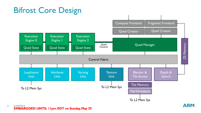
First and foremost, a single Bifrost core contains 3 quad execution engines. This means that a single core is at any time executing up to 12 FMAs, spread over the aforementioned 3 quads. These quads are in turn fed by the core’s thread management frontend (now called a Quad Manager), which combined with the other frontends issues work to all of the functional units throughout the core.
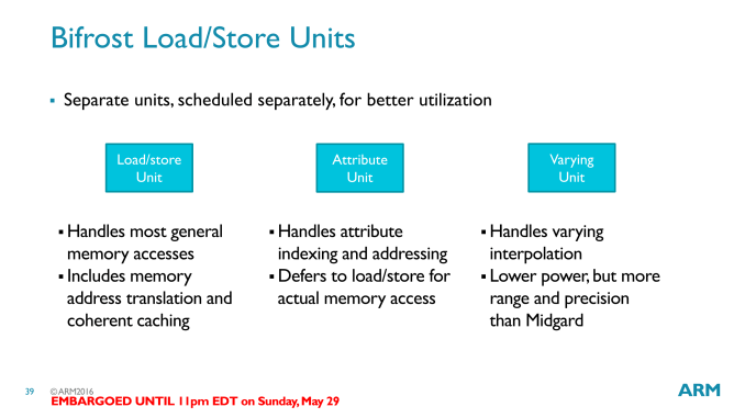
As we’ve now seen the quad execution engines, insightful readers might have noticed that the execution engines are surprisingly sparse. They contain ALUs, register files, and little else. In most other architectures – including Midgard – there are more functional units organized within the execution engines, and this is not the case for Bifrost. Instead the load/store unit, texture unit, and other units have been evicted from the execution engines and placed as separate units along the control fabric.
Along with the shift from ILP to TLP, this is one of the more significant changes in Bifrost as compared to Midgard. Not unlike the TLP shift then, much of this change is driven by resource utilization. These units aren’t used as frequently as the ALUs, and this is especially the case as shader programs grow in length. As a result rather than placing this hardware within the execution engines and likely having it underutilized, ARM has moved them to separate units that are shared by the whole core.
The one risk here is now that there’s contention for these resources, but in practice it should not be much of an issue. Comparatively speaking, this is relatively similar to NVIDIA’s SMs, where multiple blocks of ALUs share load/store and texture units. Meanwhile this should also simplify core design a bit; only a handful of units have L2 cache data paths, and all of those units are now outside of execution engines.
Overall these separated units are not significantly different from their Midgard counterparts, and the big change here is merely their divorce from the execution engines. The texture unit, for example, still offers the same basic feature sets and throughput as Midgard’s, according to ARM.
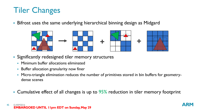
Meanwhile something that has seen a significant overhaul compared to Midgard is ARM’s geometry subsystem. Bifrost still uses hierarchical tiling to bin geometry into tiles to work on it. However ARM has gone through quite a bit of effort here to reduce the memory usage of the tiler, as high resolution screens and higher geometry complexity was pushing up the memory usage of the tiler, and ultimately hurting performance and power efficiency.
Bifrost implements a much finer grained memory allocation system, one that also does away entirely with minimum allocation requirements. This keeps memory consumption down by reducing the amount of overhead from otherwise oversized buffers.
But perhaps more significant is that ARM has implemented a micro-triangle discard accelerator into Bifrost. By eliminating sub-pixel triangles that can’t be seen early on, ARM no longer needs to store those tringles in the tiler, further reducing memory needs. Overall, ARM is reporting that Bifrost’s tiler changes are reducing tiler memory consumption by up to 95%.
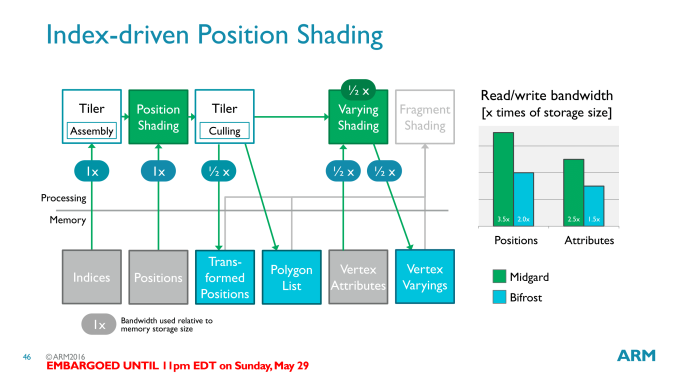
Along similar lines, ARM has also targeted vertex shading memory consumption for optimization. New to Bifrost is a feature ARM is calling Index-Driven Position Shading, which takes advantage of some of the aforementioned tiler changes to reduce the amount of memory bandwidth consumed there. ARM’s estimates put the total bandwidth savings for position shading at around 40%, given that only certain steps of the process can be optimized.
Finally, at the opposite end of the rendering pipeline we have Bifrost’s ROPs, or as ARM labels them, the blending unit and the depth & stencil unit. While these units take a similar direction as the texture unit – there are no major overhauls here – ARM has confirmed that Bifrost’s blending unit does offer some new functionality not found in Midgard’s. Bifrost’s blender can now blend FP16 targets, whereas Midgard was limited to integer targets. The inclusion of floating point blends not only saves ARM a conversion – Midgard would have to covert FP16s to integer RGBA – but the native FP16 blend means that precision/quality should be improved as well.
FP16 blends have a throughput of 1 pixel/clock, just like integer blends, so these are full speed. On that note, Bifrost’s ROP hardware does scale with the core count, so virtually every aspect of the architecture will scale up with larger configurations. Given what Mali-G71 can scale to, this means that the current Bifrost implementation can go up to 32px/clock.
Putting It Together: Mali-G71
Now that we’ve seen what Bifrost looks like at the core level, it’s time to take a look at the big picture. The first ARM GPU design that Bifrost will be going into is the high-end Mali-G71, which is being announced alongside the Cortex-A73 this morning.
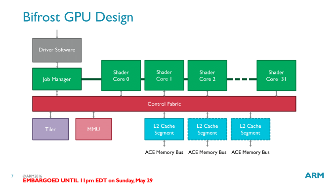
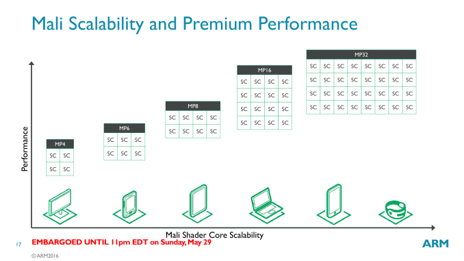
Like other Mali designs, the G71 is designed for a variable number of shader cores, up to 32 in total. This gives ARM’s clients a significant amount of scalability to work with, and ARM’s own marketing slides show an 8x span in designs, from G71MP4 all the way up to the full G71MP32. At the same time it’s not completely clear at the moment if a full sized 32 core design is even viable for a mobile device, at least on current processes. Mali’s core count scalability tends to be very forward looking in that regard.
Connecting the various shader cores together is a new control fabric for Bifrost. The new fabric goes hand-in-hand with the earlier changes we discussed to the core design, which changed how various units are attached to the fabric. There are also some implications for heterogeneous compute, which we’ll get back to in a bit.
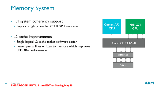
Meanwhile at the other end of the fabric is G71’s L2 cache subsystem. In a change from Midgard, the L2 cache is now a single logical L2 cache, as opposed to being a fully segmented cache before. Furthermore the cache has been reworked a bit to cut down on the number of partial lines that are flushed out to memory. Partial lines became a more pressing problem with LPDDR4, which introduced a larger prefetch size that in turn is less tolerant of partial lines.
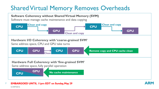
But the biggest news here where the L2 cache fits into the bigger picture in the ARM ecosystem, where it’s attached to the SoC coherent interconnect, such as ARM’s new CoreLink CCI-550 interconnect or third-party proprietary interconnect. Overall G71 now offers up to 4 full ACE (fully coherent) interfaces to the interconnect, versus only two ACE Lite (IO coherent) interfaces on Midgard. Taken altogether, thanks to a combination of architecture changes at the GPU level, the fabric level, the cache level, and the interconnect level, G71 offers full cache coherency with the rest of the system. As a result, when paired up with a suitable CPU core, G71 is capable of heterogeneous compute.
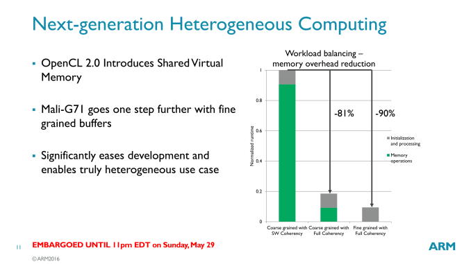
ARM has stated their intention to step into offering heterogeneous compute functionality for some time now, and G71 is in turn their first GPU to be released with support for the feature. The implementation here allows for a full “fine grained” compute, meaning that both the CPU and GPU can see each other’s caches, allowing for the greatest potential performance gains from heterogeneous compute.
From a software standpoint, it’s interesting to note that ARM has gone with an OpenCL 2.0-centric approach, intending to make the functionality accessible through that and related (SPIR-V utilizing) APIs such as Vulkan. G71 however does not support the Heterogeneous System Architecture’s HSAIL standard, this despite ARM being a member of the HSA Foundation. ARM did not have too much to say on the matter, but has stated that they never “totally bought into” HSAIL. OpenCL 2.0, by comparison, is a more generic implementation at the API level, leaving ARM to sort out the low level details as they see fit.
Update 06/01: With yesterday's announcement of the HSA 1.1 specification, I went back to ARM to ask them whether the new specification impacts the company’s heterogenous compute plans at all, especially given that their architecture doesn’t support the 1.0 standard. As it turns out, ARM is going a route very similar to AMD’s ROCm platform: while the company isn’t utilizing the HSAIL – and thus in the strictest sense isn’t a complete HSA platform – they are using the HSA standard in the development of their hardware.
At a hardware level, the HSA specification standardizes a number of aspects of the hardware for common interoperability and easier programming purposes, including signals, queues, floating point number handling, and other, low-level minutiae about how heterogeneous execution should work. This is separate from the HSAIL, which is more concerned with the software aspects of heterogeneous programming, and though helpful, is not necessary for heterogeneous compute. As a result while Mali-G71 is technically not an HSA platform, in practice it is HSA hardware, using the HSA specification as a means to offer a common and well understood execution model for heterogeneous compute. So ARM is very much on-board with HSA – and is essentially supplying one of the first non-AMD HSA 1.1 hardware designs – even if they’re not using HSAIL itself.
At this point heterogeneous compute is still a long term play for ARM. The potential performance improvements are, in the right scenarios, very significant. And using the GPU instead of the CPU is again a sound move when there’s lots of suitable parallel work to throw at it, especially in SoCs where power efficiency is so critical. But it will take time to bring software developers on board, so while the hardware will soon be here, it will take some time for the software to catch up.
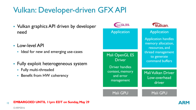
That said, a big part of the process will the natural migration towards newer APIs that better support heterogeneous execution. ARM of course has been big on Vulkan support, and while Vulkan is first and foremost a graphics API, as the line blurs between graphics and compute, it feeds into their compute plans as well. The forthcoming Vulkan 1.1 specification is set to introduce some new compute functionality that further bridges the gap between Vulkan 1.0 and OpenCL 2.x, which ARM in turn will be preparing to take advantage of.
But regardless of the compute implications, ARM sees Vulkan as being important to the long term progression of software development. The lower overhead of Vulkan factors well into the power and thermal needs of mobile devices; unnecessary CPU work not only burns power, but it eats into thermal headroom that could be going to the GPU. Consequently, expect to see ARM pushing Vulkan even harder in the coming months in alignment with G71.
Wrapping Things Up: Mali-G71, Coming Soon
Like ARM’s associated Cortex-A73 announcement, today’s Mali-G71 revelations are being made ahead of actual silicon availability. To that end a lot of ARM’s projections are based on early prototyping of manufacturing process and architectural simulations, though at this late stage those simulations tend to be pretty close.
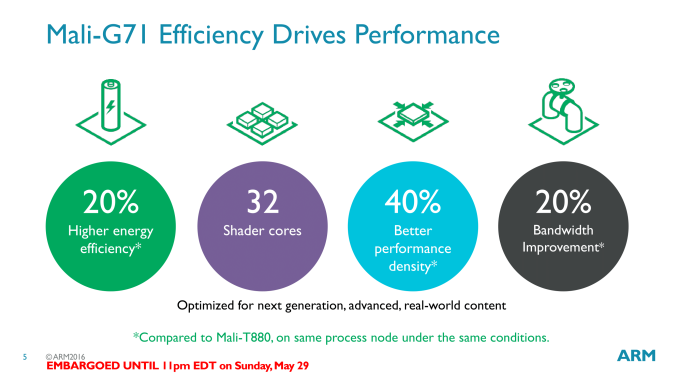
ARM’s official numbers for G71 call for it to offer significant improvements over a same-process Mali-T880 with respect to both energy efficiency and density. For the former ARM is expecting G71 to deliver 20% better energy efficiency over T880, and on the latter to offer 40% better performance density – or in other words, the same performance at 40% less die space. Though ARM has not been heavily penalized for area efficiency, the latter has been one of the few areas where they haven’t done quite as well, and is something competitor Qualcomm is keen to call them out on.
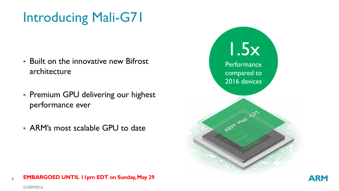
From a performance standpoint, ARM is expecting G71-based devices to offer around 1.5x the performance of current, T880 devices. This is a slightly fuzzier metric – it’s not 50% faster at the same MP configuration – but rather a combination of manufacturing improvements, a larger number of shader cores, and Bifrost architectural improvements. Andrei also suspects that if we were looking at apples-to-apples ISO-power/ISO-area numbers where everything was held equal, the actual performance gains would be even greater.
With all of that said, expect to see G71 operate a lot like a drop-in replacement for current Mali GPUs when it comes to graphics. Bifrost is an architectural update for Mali rather than a feature update. There are no major graphics features that G71 supports that T880 does not; both deliver on the same OpenGL ES and Vulkan graphics functionality. The heterogeneous compute functionality on the other hand stands to make a big impact for general compute tasks, just not for graphics.
Ultimately what this gets ARM is a chance to recalibrate their architecture for the future, to better align with both what software developers are writing and what device manufacturers need in their GPUs. Bifrost is the new modern Mali, and the shift to a TLP-centric design should serve ARM well in the future based on what we’ve seen similar shifts do for AMD and others. Meanwhile the overall performance gains will allow ARM and its customers to hedge their bets on things such as 4K phones and mobile VR, giving them a more suitable GPU design to use if those innovations prove popular.
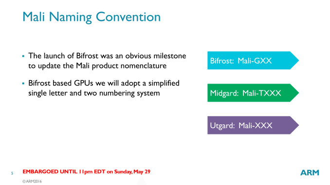
Wrapping things up, while ARM is only announcing the Mali-G71 today, the company has clearly left the door open to future GPU designs. As a high-end GPU design, G71 is the immediate successor to the T880, but I expect in time that ARM will want to produce GPU designs suitable to replace Mali T820 and the like. That ARM started at G71 is a good hint of what’s to come; future Bifrost GPUs will use the two digit G numbering scheme, so you can easily see where future GPUs may slot in.

