Original Link: https://www.anandtech.com/show/7793/imaginations-powervr-rogue-architecture-exposed
Imagination's PowerVR Rogue Architecture Explored
by Ryan Smith on February 24, 2014 3:00 AM EST- Posted in
- GPUs
- Imagination Technologies
- PowerVR
- PowerVR Series6
- SoCs

When it comes to our coverage of SoCs, one aspect we’ve been trying to improve on for some time now is our coverage and understanding of the GPU portion of those SoCs. In the PC space we’re fortunate that there are just three major players – Intel, NVIDIA, and AMD – and that all three of them have over the years learned how to become very open and forthcoming about their GPU architectures. As a result we’ve had a level of access that has allowed us to better understand PC GPUs in a way that in earlier times simply wasn’t possible.
In the SoC space however we haven’t been so fortunate. Our understanding of most SoC GPU architectures has not been nearly as deep due to the fact that SoC GPU designers have been less willing to come forward with public details about their architectures and how those architectures have evolved over the years. And this has been for what’s arguably a good reason – unlike the PC GPU space, where only 2 of the 3 players compete in either the iGPU or dGPU markets, in the SoC GPU space there are no fewer than 7 players, all of whom are competing in one manner or another: NVIDIA, Imagination Technologies, Intel, ARM, Qualcomm, Broadcom, and Vivante.
Some of these players use their designs internally while others license out their designs as IP for inclusion in 3rd party SoCs, but all these players are in a much more competitive market that is in a younger place in its life. All the while SoC GPU development still happens at a relatively quick pace (by GPU standards), leading to similarly quick turnarounds between GPU generations as GPU complexity has not yet stretched out development to a 3-4 year process. As a result of SoC GPUs still being a young and highly competitive market, it’s a foregone conclusion that there is still a period of consolidation ahead of us – not unlike what has happened to SoC integrators such as TI – which provides all the more reason for SoC GPU players to be conservative about providing public details about their architectures.
With that said, over the years we have made some progress in getting access to the technical details, due in large part to the existing openness policies of NVIDIA and Intel. Nevertheless, as two of the smaller players in the mobile GPU space this still leaves us with few details on the architectures behind the majority of SoC GPUs. We still want more.
This brings us to today. In what should prove to be an extremely eventful and important day for our coverage and understanding of SoC GPUs, we’d like to welcome Imagination Technologies to the “open architecture” table. Imagination chosen to share more details about the inner workings of their Rogue Series 6 and Series 6XT architectures, thereby giving us our first in-depth look at the architecture that’s powering a number of high-end products (not the least of which is all of Apple’s current-gen products) and descended from some of the most widely used SoC GPU designs of all time.

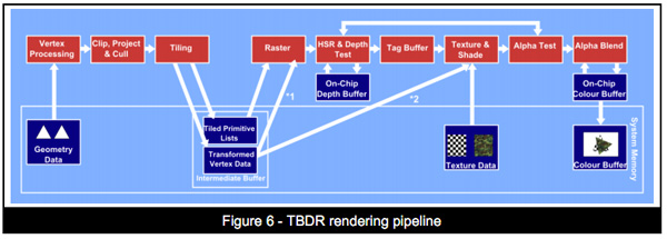
Now Imagination is not going to be sharing everything with us today. The bulk of the details Imagination is making available relate to their Unified Shading Cluster (USC) shading block, the heart of the Series 6/6XT GPUs. They aren’t discussing other aspects of their designs such as their geometry processors, cache structure, or Tile Based Deferred Rendering system – the company’s secret sauce and most potent weapon for SoC efficiency – but hopefully one day we’ll get there. In the meantime we will have our hands full just taking our first look at the Series 6/6XT USCs.
Finally, before we begin we’d like to thank Imagination for giving us this opportunity to evaluate their architecture in such great detail. We’ve been pushing for this for quite some time, so we’re pleased that this is coming to pass.
Imagination is publishing a pair of blogs and pseudo whitepapers on their website today: Graphics cores: trying to compare apples to apples, and PowerVR GX6650: redefining performance in mobile with 192 cores. Along with this they have also been answering many of our deepest technical questions, so we should have a good handle on the Rogue USC. So with that in mind, let’s dive in.
Background: How GPUs Work
Seeing as how this is our first in-depth architecture article on a SoC GPU design (specifically as opposed to PC-derived designs like Intel and NVIDIA), we felt it best to start at the beginning. For our regular GPU readers the following should be redundant, but if you’ve ever wanted to learn a bit more about how a GPU works, this is your place to start.
GPUs, like most complex processors, are composed of a number of different functional units responsible for the different aspects of computation and rendering. We have functional units that setup geometry data, frequently called geometry engine, geometry processors, or polymorph engines. We have memory subsystems that provide caching and access to external memory. We have rendering backends (ROPs or pixel co-processors) that take computed geometry and pixels to blend them and finalize them. We have texture mapping units (TMUs) that fetch textures and texels to place them within a scene. And of course we have shaders, the compute cores that do much of the heavy lifting in today’s games.
Perhaps the most basic question even from a simple summary of the functional units in a GPU is why there are so many different functional units in the first place. While conceptually virtually all of these steps (except memory) can be done in software – and hence done in something like a shader – GPU designers don’t do that for performance and power reasons. So-called fixed function hardware (such as ROPs) exists because it’s far more efficient to do certain tasks with hardware that is tightly optimized for the job, rather than doing it with flexible hardware such as shaders. For a given task flexible hardware is bigger and consumes more power than fixed function hardware, hence the need to do as much work in power/space efficient fixed function hardware as is possible. As such the portions of the rendering process that need flexibility will take place in shaders, while other aspects that are by their nature consistent and fixed take place in fixed function units.
The bulk of the information Imagination is sharing with us today is with respect to shaders, so that’s what we’ll focus on today. On a die area basis and power basis the shader blocks are the biggest contributors to rendering. Though every functional unit is important for its job, it’s in the shaders that most of the work takes place for rendering, and the proportion of that work that is bottlenecked by shaders increases with every year and with every generation, as increasingly complex shader programs are created.
So with that in mind, let’s start with a simple question: just what is a shader?
At its most fundamental level, a shader core is a flexible mathematics pipeline; it is a single computational resource that accepts instructions (a shader program) and executes it in order to manipulate the pixels and polygon vertices within a scene. An individual shader core goes by many names depending on who makes it: AMD has Stream Processors, NVIDIA has CUDA cores, and Imagination has Pipelines. At the same time how a shader core is built and configured depends on the architecture and its design goals, so while there are always similarities it is rare that shader cores are identical.
On a lower technical level, a shader core itself contains several elements. It contains decoders, dispatchers, operand collectors, results collectors, and more. But the single most important element, and the element we’re typically fixated on, is the Arithmetic Logic Unit (ALU). ALUs are the most fundamental building blocks in a GPU, and are the base unit that actually performs the mathematical operations called for as part of a shader program.
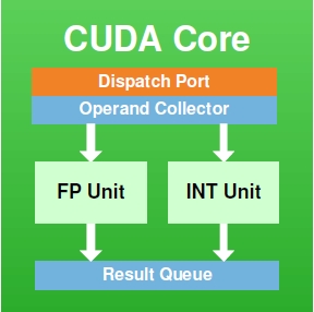
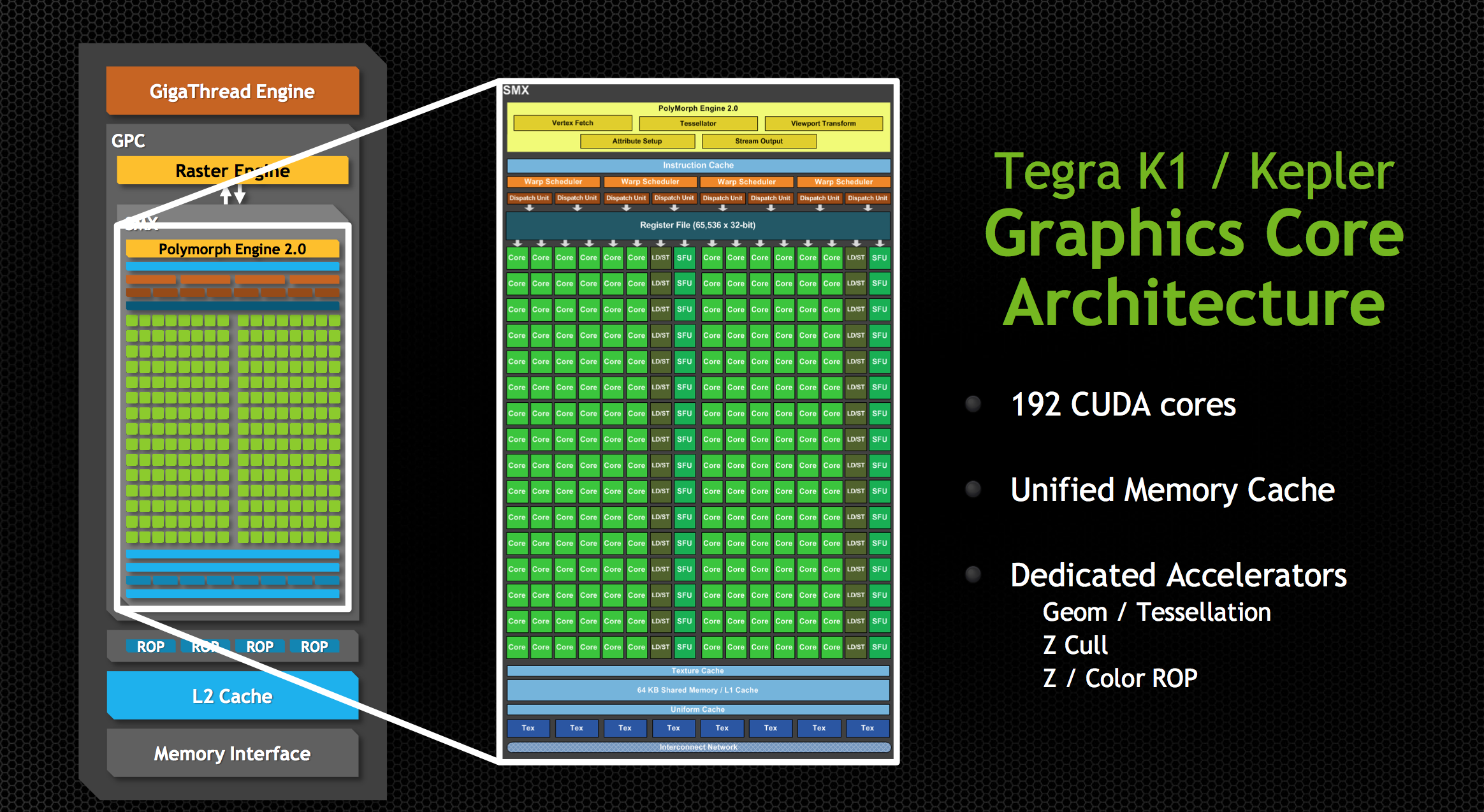
An NVIDIA CUDA Core
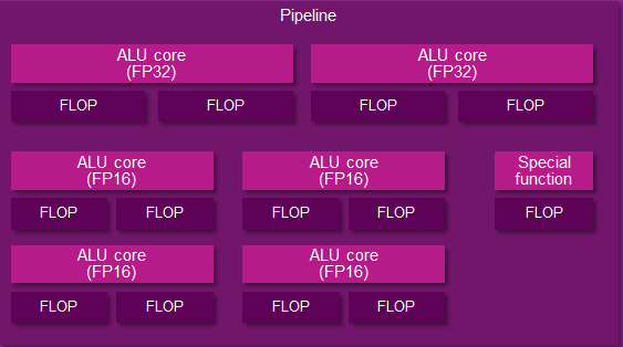
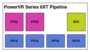
And an Imgination PVR Rogue Series 6XT Pipeline
The number of ALUs within a shader core in turn depends on the design of the shader core. To use NVIDIA as an example again, they have 2 ALUs – an FP32 floating point ALU and an integer ALU – either of which is in operation as a shader program requires. In other designs such as Imagination’s Rogue Series 6XT, a single shader core can have up to 7 ALUs, in which multiple ALUs can be used simultaneously. From a practical perspective we typically count shader cores when discussing architectures, but it is at times important to remember that the number of ALUs within a shader core can vary.
When it comes to shader cores, GPU designs will implement hundreds and up to thousands of these shader cores. Graphics rendering is what we call an embarrassingly parallel process, as there are potentially millions of pixels in a scene, most of which can be operated in in a semi-independent or fully-independent manner. As a result a GPU will implement a large number of shader cores to work on multiple pixels in parallel. The use of a “wide” design is well suited for graphics rendering as it allows each shader core to be clocked relatively low, saving power while achieving work in bulk. A shader core may only operate at a few hundred megahertz, but because there are so many of them the aggregate throughput of a GPU can be enormous, which is just what we need for graphics rendering (and some classes of compute workloads, as it turns out).
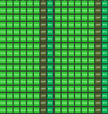
A collection of Kepler CUDA cores, 192 in all
The final piece of the puzzle then is how these shader cores are organized. Like all processors, the shader cores in a GPU are fed by a “thread” of instructions, one instruction following another until all the necessary operations are complete for that program. In terms of shader organization there is a tradeoff between just how independent a shader core is, and how much space/power it takes up. In a perfectly ideal scenario, each and every shader core would be fully independent, potentially working on something entirely different than any of its neighbors. But in the real world we do not do that because it is space and power inefficient, and as it turns out it’s unnecessary.
Neighboring pixels may be independent – that is, their outcome doesn’t depend on the outcome of their neighbors – but in rendering a scene, most of the time we’re going to be applying the same operations to large groups of pixels. So rather than grant the shader cores true independence, they are grouped up together for the purpose of having all of them executing threads out of the same collection of threads. This setup is power and space efficient as the collection of shader cores take up less power and less space since they don’t need the intelligence to operate completely independently of each other.

The flow of threads within a wavefront/warp
Not unlike the construction of a shader core, how shader cores are grouped together will depend on the design. The most common groupings are either 16 or 32 shader cores. Smaller groupings are more performance efficient (you have fewer shader cores sitting idle if you can’t fill all of them with identical threads), while larger groupings are more space/power efficient since you can group more shader cores together under the control of a single instruction scheduler.
Finally, these groupings of threads can go by several different names. NVIDIA uses the term warp, AMD uses the term wavefront, and the official OpenGL terminology is the workgroup. Workgroup is technically the most accurate term, however it’s also the most ambiguous; lots of things in the world are called workgroups. Imagination doesn’t have an official name for their workgroups, so our preference is to stick with the term wavefront, since its more limited use makes it easier to pick up on the context of the discussion.
Summing things up then, we have ALUs, the most basic building block in a GPU shader design. From those ALUs we build up a shader core, and then we group those shader cores into a array of (typically) 16 or 32 shader cores. Finally, those arrays are fed threads of instructions, one thread per shader core, which like the shader cores are grouped together. We call these thread groups wavefronts.
And with that behind us, we can now take a look at the PowerVR Series 6/6XT Unfied Shading Cluster.
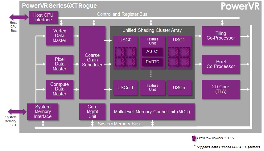
Imagination’s PowerVR Rogue Series 6/6XT USCs Dissected
Diving right into the heart of the matter, it’s probably best to start with a partial explanation for why Imagination is being so forward about their architecture after all this time.
Imagination’s principle blog, Graphics cores: trying to compare apples to apples, opens up with an argument over just what a “core” is and how it should be counted. Imagination doesn’t name any names, but from the context of their blog it’s clear that they’re worried about being in a core war and losing based on who’s counting cores and how. Time and time again we’ve seen chip and device makers promote their products both by their clockspeeds and their number of cores, leading to both MHz wars and core wars.
Both of these pieces of data are in fact absolutely essential to understanding a product, but consumers – rightfully disinterested in needing a Comp. Engineering degree to understand their purchases – will latch on to one or both numbers, which in turn rewards whoever can push a product with the highest clockspeed or the highest number of cores. The latter in turn can result in some very creative accounting, such as the Motorola X8, where components that aren’t traditionally called a core end up in the core count.
In the SoC GPU space there thankfully isn’t any creative accounting going on, but the nature of the Rogue architecture combined with Imagination’s previous method of counting cores has left Imagination shooting themselves in the foot if they were to get into a core war. If nothing else, the fact that Imagination has previously uses the term “core” to define a single USC, which depending on the specific design may be replicated several times, means that they end up having relatively low core counts.
Compounding that matter is that at a pipeline or shader core level (there’s that word again), Rogue has several FP32 (or FP16) ALUs when other architectures may only have one. So even if one were to count pipelines, Imagination would come up with just 16 cores in a USC.
Their competition and impetus – and again Imagination hasn’t named any names – would appear to be NVIDIA, who just recently announced their Tegra K1 SoCs. A K1 contains 192 CUDA cores, each much narrower than a Rogue pipeline. So even though a high-end Rogue design would have 6 or so USCs, that would only be 96 pipelines versus 192 CUDA cores. Imagination clearly doesn’t want to be dismissed based on this metric, hence their interest in arguing what a core is, and more importantly part of the reason for their desire to open up and discuss their architecture so that we can understand why this difference matters. Imagination may only have 96 pipelines, but they have many more ALUs in each one of those pipelines.
The Rogue
And that brings us to the Rogue architecture. For today’s article and blog releases, Imagination has given us some surprisingly deep details on the Rogue USC, from which we can finally paint a picture of how thread execution works on Rogue, and furthermore gather some idea on what Rogue’s strengths are and what weaknesses it faces.
We’ll begin with differentiating between Rogue as in PowerVR Series 6, and Series 6XT. Series 6XT was the recently announced refresh for the Series 6 family, intending to further improve on PowerVR performance by undertaking several optimizations to the design. At the time of that announcement we didn’t have very many details on what those optimizations were, and now we have a much better idea.

It turns out that Imagination has been doing some tinkering under the hood, and while the number of FP32 slots remains unchanged, the FP16 slots have been altered. Wait, did we say FP16 slots?! Oh yes!
It’s a shame we don’t have such similar low level details for other SoC architectures, but from a PC perspective it’s extremely interesting that Imagination has FP16 slots. As a quick refresher, on the PC side GPUs have been using FP32 operations exclusively for quite some time, and all ALUs have been FP32 for years. But of course mobile trails PC in functionality and shader complexity, so while FP16 usage is rarer in PC games and applications, it can be very common in the mobile space.
The tradeoff of course is performance for accuracy. A 16bit floating point number is pretty imprecise – a 16bit value only gives us 65K combinations – hence it’s rarely used in the PC space in favor of far more accurate 32bit floating point numbers, which offer 4 billion combinations. But a 16bit value is smaller than a 32bit value, requiring less memory to store, less bandwidth to move, less energy to compute, and fewer transistors to operate on. So in the mobile space FP16 is still in use, both on the software side and the hardware side, with developers taking care not to let the lower precision cause rendering errors.
The interesting part on the hardware side is the implementation of dedicated FP16 units, versus just running the values on FP32 units. In the PC space we do the latter, but of course FP16 operations are relatively rare. The catch being that it’s not the most efficient way to execute FP16 operations; we’re firing up a lot of extra transistors and burning extra power to do it. In the PC space this is a reasonable tradeoff, but in the mobile space it’s clear the Imagination has decided otherwise.
The end result being that Rogue has dedicated FP16 units, not unlike how NVIDIA has dedicated FP64 CUDA cores on their desktop architectures. FP16 units take up additional die space – you have to place them alongside your FP32 units – but when you need to compute an FP16 number, you don’t have to fire up a more expensive FP32 unit to do the work. Hence the inclusion of FP16 units is a tradeoff between die size and performance, with the additional performance coming from the reduction in power consumption and heat when operating on FP16 values.
That little segue aside, let’s get back to the difference between Series 6 and Series 6XT. With Series 6, Imagination has an interesting setup where their FP16 ALUs can process up to 3 operations in one cycle.
As a refresher, for a more traditional ALU we say that one ALU can achieve 2 FLOPs in one cycle because we typically count the most dense operation, the Multiply Addition (MAD), otherwise seen as a Multiply Accumulate (MAC) or Fused Multiply Addition (FMA). MAD is a special case where one ALU can do the multiply and the accumulate in one cycle, one of a handful of scenarios where multiple operations can occur at once. MADs and their variants are relatively common in graphics work, hence for GPU performance this is the number we usually quote as it’s especially useful in graphics, and being the bigger number it also makes manufacturers happier, too.
With that said, Imagination’s FP16 ALUs are more intricate than their FP32 ALUs, especially under Series 6. Unfortunately Imagination is unable to share the complete details with us of why this is (as we've noted before, they’re not yet fully open), but it’s clear from this diagram that the Series 6 FP16 ALU has been optimized for some kind of 3 operator instruction. What that operation is we don’t know, but presumably it was important enough for Imagination to give their FP16 ALUs the ability to do it in one cycle.
But from the perspective of an individual pipeline it’s interesting to see that with Series 6XT Imagination has shaken things up by "adding" 2 more FP16 ALUs. Keeping in mind that these are logical diagrams and not physical diagrams – in reality these ALUs are almost certainly tied together in a limited fashion rather than standing alone – Imagination has changed it so that Series 6XT can process more 2 operator FP16 instructions such as MAD. Without more details it’s hard to say for sure what’s going on, but if these “new” FP16 ALUs are really just modifications of the old FP16 ALUs, then it would be a safe assumption that Imagination can still execute their 3 operator instructions over what’s logically 2 ALUs, making these new FP16 ALUs a wider variant of the previous ALU.
Otherwise from this point of view Series 6 and Series 6XT are nearly identical. We have the 2 FP32 ALUs, and then for special functions – transcendentals and the like – a dedicated special function unit exists off to the side. On that note, for the rest of this article we will primarily be focusing on Series 6XT since it’s the newer architecture, but with the exception of FP16 operations it will be equally applicable to both Series 6 and 6XT.
How Rogues Get Executed: Wavefronts & Superscalar ILP
Now that we’ve seen the basic makeup of a single Rogue pipeline, let’s expand our view to the wider USC.
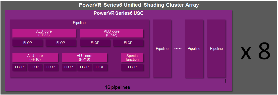
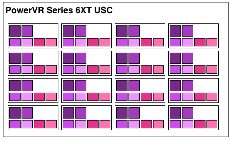
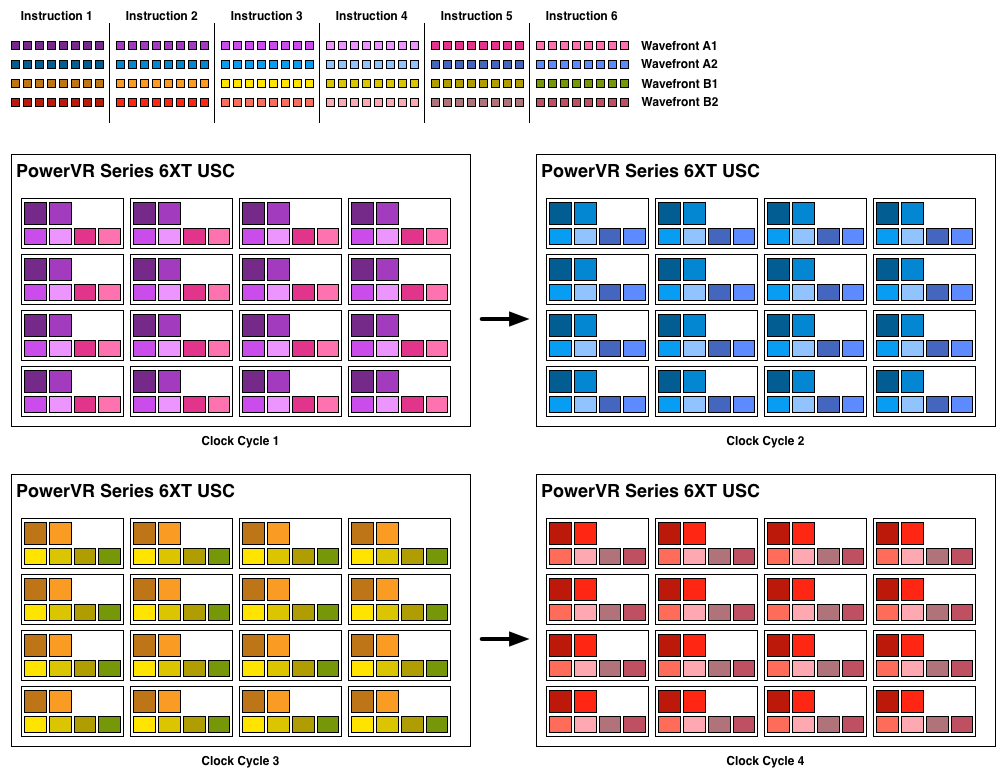
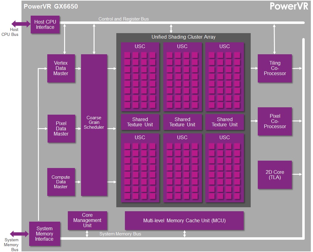
A single Rogue USC is comprised of 16 pipelines, making the design a 16 wide array. This, along with a texture unit, comprises one “cluster” when we’re talking about a multi-cluster (multiple USC) Rogue setup. In a setup with multiple USCs, the texture unit will then be shared among a pair of USCs.
We don’t have a great deal of information on the texture units themselves, but we do know that a Rogue texture unit can fetch 4 32bit bilinear texels per clock. So for a top-end 6 USC part, we’d be looking at a texture rate of 12 texels/clock.
Now by PC standards the Rogue pipeline/USC setup is a bit unusual due to its width. Both AMD and NVIDIA’s architectures are fairly narrow at this level, possessing just a small number of ALUs per shader core/pipeline. The impact of this is that by having multiple ALUs per pipeline in Rogue’s case, there is a need to extract some degree of instruction level parallelism (ILP) out of threads to feed as many ALUs as possible. Extracting ILP in turn requires having instructions in a single thread that have no dependencies on each other that can be executed in parallel. This can be many (but not all) instructions, so it’s worth noting that the efficiency of a USC is going to depend in part on the instructions in a thread. We call this property a superscalar design.
For the sake of comparison, AMD’s Graphics Core Next is not a superscalar design at all, while NVIDIA’s Kepler is superscalar in a similar manner. NVIDIA’s CUDA cores only have 1 FP32 ALU per core, but there are additional banks of CUDA cores that can be co-issued additional instructions, conditions permitting. So Rogue has a similar reliance on ILP within a thread, needing it to achieve maximum efficiency.
What makes Rogue all the more interesting is just how wide it is. For FP32 operations it’s only 2-wide, but if we throw in the FP16 operations we’re technically looking at a 6-wide design. The odds of having FP16 and FP32 operations ready to co-issue in such a manner is far rarer than having just a pair of FP32 instructions to co-issue, so again Rogue technically is very unlikely to achieve 100% utilization of a pipeline.
That said, the split between FP16 and FP32 units makes it clear that Imagination expects to be using one or the other most of the time rather than both, so as far as the design goes this is not unexpected. For FP32 instructions then it’s a simpler 2-wide setup, while FP16 instructions are going to be trickier as full utilization of FP16 is going to require a full 4 instruction setup (say 4 MADs following each other). The fact that Series 6XT has 4 FP16 units despite that is interesting, as it implies that it was worth the extra die space compared to the Series 6 setup of 2 FP16 units.
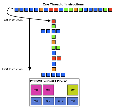
With that out of the way, let’s talk about how work is dispatched to the pipelines within a USC. Each pipeline works on one thread at a time, the same as any other modern GPU architecture. Consequently we’d expect the wavefront size to be 16 threads.
However there’s an interesting fact that we found out about the USCs, and that is that they don’t run at the same clockspeed throughout. The ALUs themselves run at the published clockspeed for the GPU, but the frontends that feed them – the decoders and operand collectors do not. Imagination has not specified at what rate they run at, but the only thing that makes sense is ½ the rate of the ALUs. So a 300MHz USC would have its decoder frontend running at 150MHz, etc.
An example of a wavefront executing. Instructions per thread not to scale
Consequently we believe that the size of a wavefront is not 16 threads, but rather 32 threads, executed over 2 cycles of the ALUs. This is not the first time we’ve seen this design – NVIDIA did something similar for their retired Fermi architecture – but this isn’t something we were expecting to see again. But with the idiosyncrasies of the SoC space, this is apparently something that still makes sense. Imagination did tell us that there are tangible power savings from doing this, and since SoC GPUs are power limited in most cases anyhow, this is essentially the higher performance option. Go faster by going slower.
Finally, this brings us to the highest level, the USC array. Each USC in an array receives its own thread to work on, so the number of threads actively being executed will be identical to the number of USCs in a design. For a high-end 6 module design, we’d be looking at 6 threads, whereas for a smaller 2 module design it would be just 2 threads.
Technical Comparisons
Finally, to close out this look at the Rogue architecture we wanted to spend a bit of time looking at how it compares to other architectures. Unfortunately the lack of details we have on other SoC GPU architectures means we can’t make any meaningful comparisons there beyond the GFLOPs comparisons we do today (and that says nothing of real world efficiency). But we can compare it to the next best thing, which is mobile parts based on desktop GPU architectures from AMD and NVIDIA. The latter case being especially interesting, as we know Kepler will be coming to SoCs with the K1.
With that said, and we can’t reiterate this enough, this is just a look at theoretical performance. It is not possible to take into account efficiency measures such as memory bandwidth, ROPs, or especially early rejection optimizations such as Tile Based Deferred Rendering. TBDR is Imagination’s ace, and while other GPU firms have their own early rejection technologies, from what little we know about each of them, none of them quite matches TBDR. So Rogue’s theoretical performance aside, if Imagination is rejecting significantly more work before it hits their shaders, then they would have greater performance when all other factors were held equal. The only way to compare the real world performance of these architectures is to benchmark their real world performance, so please do not consider this the final word on performance.
For this comparison we’ll be looking at NVIDIA’s Kepler based K1, AMD’s GCN based A4-1350, and Imagination’s Rogue based GX6650 and G6230. Because Rogue is offered in multiple configurations it’s difficult to determine just how large a Rogue configuration would equal K1 or A4-1350 from a performance and size perspective, but given the anticipated integration time for Series 6XT, a 6 cluster configuration seems the most likely.
| GPU Specification Comparison | |||||||
| NVIDIA K1 | Imagination PVR GX6650 | Imagination PVR G6230 | AMD A4-1350 | NVIDIA GTX 650 | |||
| FP32 ALUs | 192 | 192 | 64 | 128 | 384 | ||
| FP32 FLOPs | 384 | 384 | 128 | 256 | 768 | ||
| Pixels/Clock (ROPs) | 4 | 12 | 4 | 4 | 16 | ||
| Texels/Clock | 8 | 12 | 4 | 8 | 32 | ||
| GFLOPS @ 300MHz | 115.2 GFLOPS | 115.2 GFLOPS | 38.4 GFLOPS | 76.8 GFLOPS | 230.4 GFLOPS | ||
| Architecture | Kepler | Rogue (6XT) | Rogue (6) | GCN 1.0 | Kepler | ||
Briefly, we can see that as far as theoretical shading performance is concerned, both the GX6650 and K1 are neck-and-neck when clockspeeds are held equal. Both of them have the same ILP dependency, so both need to be able to pull off some FP32 co-issued instructions if they are to achieve their full 384 FLOP/cycle throughput. The A4-1350 on the other hand has no such limitation, making it easier to hit its 256 FLOP/cycle throughput, but never getting the chance to go past it.
Meanwhile it was surprising to see that GX6650’s theoretical pixel throughput was so high. 12 pixels/clock (12 ROPs) is much higher than either K1 or A4-1350, and in fact is quite high for an SoC class product. Most designs use relatively few ROPs here for size and power reasons, and not all designs replicate the ROPs with the shader blocks. So having 12 ROPs here was unexpected. At the same time it remains to be seen how well real world efficiency tracks this, as ROPs are frequently memory bandwidth constrained, which makes such a large number of ROPs harder to feed.
Moving on to quickly compare texture throughput, again it’s surprising to see just how many texels GX6650 can push. TMUs regularly scale with shader core counts, so the fact that it’s three-fold what a single TMU design can do is not unexpected, but until now we had never realized just what that meant for overall texture throughput. 12 texels/clock is (thankfully) a lot of texels for a SoC GPU. That said, this is also a memory bandwidth heavy operation, so it’s difficult to say how real world performance will track it.
Finally, to throw in a true desktop comparison for the fun of it, we also put NVIDIA’s Kepler based GTX 650 in the chart. Clockspeeds aside, the best case scenario for even GX6650 is that it achieves half the shading throughput as GTX 650. The ROP throughput gap on the other hand is narrower (but GTX 650 will easily have 2x the memory bandwidth) and the texture throughput gap is nearly 3x wider. In practice it would be difficult to imagine the GX6650 being any closer than about 40% of the GTX 650’s performance, once again owing to the massive memory bandwidth difference between an SoC and a discrete GPU.
Final Words
Wrapping up this architectural overview of Imagination’s Rogue architecture, it’s exciting to finally see much of the underpinnings of an SoC GPU design. While we haven’t seen every facet of Rogue yet – and admittedly it’s unlikely we ever will – the information that we’ve received on Rogue so far has given us a much better perspective on how Imagination’s latest graphics architecture works, and for that matter how Series 6 and Series 6XT differ from one-another.
Ultimately we still can’t do true apples-to-apples comparisons with these integrated GPUs (we can’t separate the CPU and memory controller from the GPU), but it should be helpful for better understanding why certain products perform the way they do, and determining what the stronger products might be in the long run. So it’s with some hope and a bit of luck that this might get the ball rolling with the other SoC GPU vendors, getting them to open up their doors a bit more so that we can see what’s inside their designs.
Coming back full circle to Imagination, we’re left with one of the big reasons why they’re opening up in the first place: core wars. Imagination is keen on not being seen as being left behind on core counts, and while we don’t expect the “core” terminology to go away any time soon, now that we have these low level Rogue architecture details, we can agree that Imagination does have a salient point as far as counting cores and ALUs is concerned.
For the purposes of FP32 operations a Rogue USC is essentially equivalent to a 32 core design, with an ILP reliance similar to what we’re seeing out of NVIDIA right now, though perhaps greater than some other designs. Or as Imagination likes to compare it to, a 6 USC design would be equivalent to a 192 core design. This speaks nothing of real world performance – without real world hardware it can’t, there are too many external variables – but it does give us an idea of how many clusters Imagination’s customers would need to achieve various degrees of theoretical performance, including what it would take to beat the competition.


