Original Link: https://www.anandtech.com/show/7677/amd-kaveri-review-a8-7600-a10-7850k
AMD Kaveri Review: A8-7600 and A10-7850K Tested
by Ian Cutress & Rahul Garg on January 14, 2014 8:00 AM EST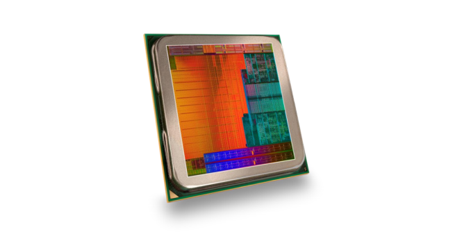
The first major component launch of 2014 falls at the feet of AMD and the next iteration of its APU platform, Kaveri. Kaveri has been the aim for AMD for several years, it's actually the whole reason the company bought ATI back in 2006. As a result many different prongs of AMD’s platform come together: HSA, hUMA, offloading compute, unifying GPU architectures, developing a software ecosystem around HSA and a scalable architecture. This is, on paper at least, a strong indicator of where the PC processor market is heading in the mainstream segment. For our Kaveri review today we were sampled the 45/65W (cTDP) A8-7600 and 95W A10-7850K Kaveri models. The A10-7850K is available today while the A8 part will be available later in Q1.
The Kaveri Overview
To almost all users, including myself up until a few days ago, Kaveri is just another iteration of AMD’s APU line up that focuses purely on the integrated graphics side of things, while slowly improving the CPU side back to Thuban levels of performance. Up until a few days ago I thought this too, but Kaveri is aiming much higher than this.
Due to the way AMD updates its CPU line, using the ‘tick-tock’ analogy might not be appropriate. Kaveri is AMD’s 3rd generation Bulldozer architecture on a half-node process shrink. Kaveri moves from Global Foundries' 32nm High-K Metal Gate SOI process to its bulk 28nm SHP (Super High Performance) process. The process node shift actually explains a lot about Kaveri's targeting. While the 32nm SOI process was optimized for CPU designs at high frequency, GF's bulk 28nm SHP process is more optimized for density with a frequency tradeoff. AMD refers to this as an "APU optimized" process, somewhere in between what a CPU and what a GPU needs. The result is Kaveri is really built to run at lower frequencies than Trinity/Richland, but is far more dense.
Kaveri is the launch vehicle for AMD's Steamroller CPU architecture, the 3rd iteration of the Bulldozer family (and second to last before moving away from the architectural detour). While Piledriver (Trinity/Richland) brought Bulldozer's power consumption down to more rational levels, Steamroller increases IPC. AMD uses Steamroller's IPC increase to offset the frequency penalty of moving to 28nm SHP. AMD then uses the density advantage to outfit the design with a substantially more complex GPU. In many senses, Kaveri is the embodiment of what AMD has been preaching all along: bringing balance to the CPU/GPU split inside mainstream PCs. The strategy makes a lot of sense if you care about significant generational performance scaling, it's just unfortunate that AMD has to do it with a CPU architecture that puts it at a competitive deficit.
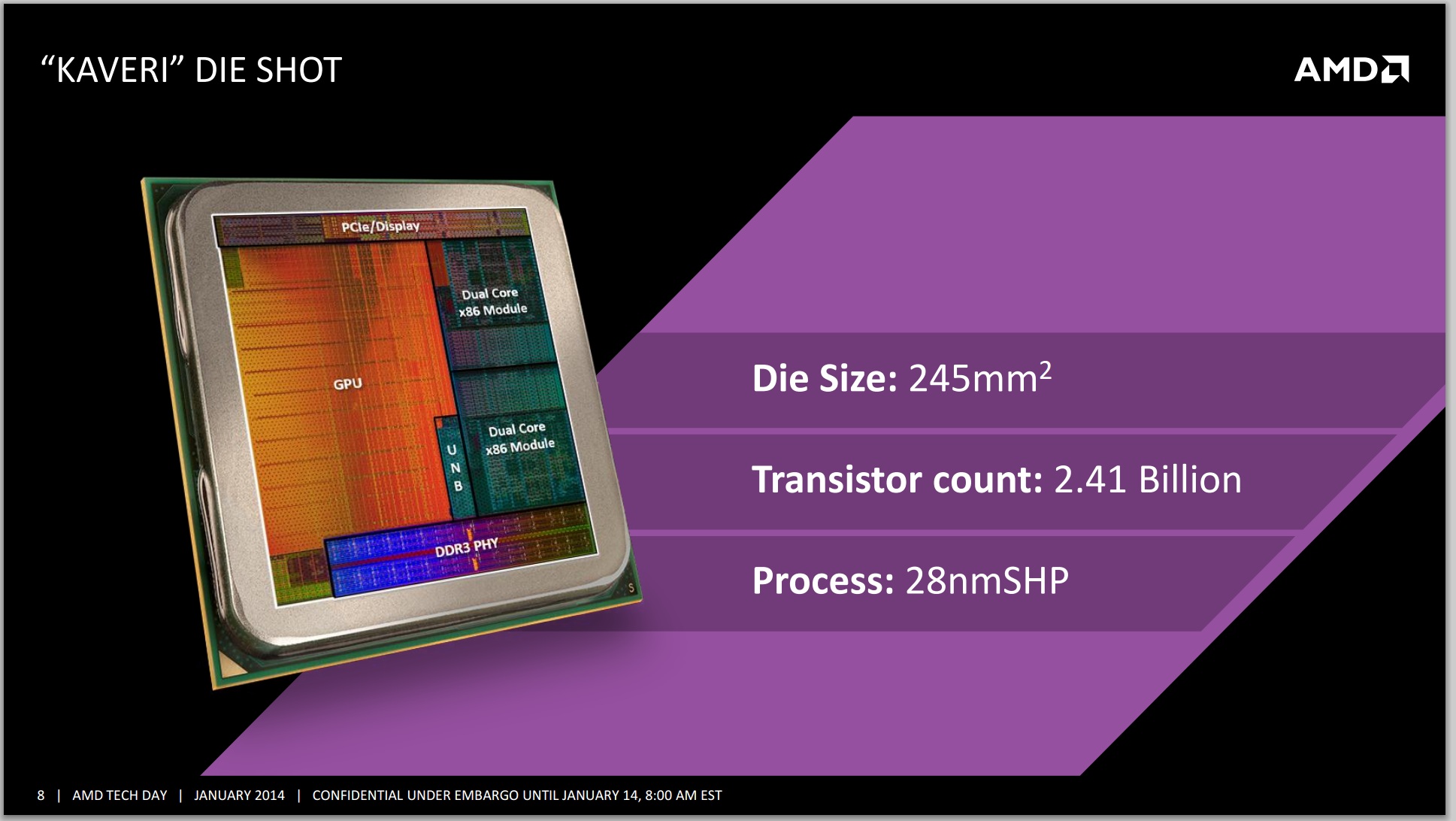
The die of Kaveri is of similar size to Richland (245mm2 vs 236mm2) but has 85% more transistors (2.41B vs. 1.3B). Unfortunately AMD hasn't confirmed whether we are talking about layout or schematic transistors here, or even if both figures are counted the same way, but there's clearly some increase in density. Typically a move from 32nm to 28nm should give a 26% boost for the same area, not an 85% boost.
The GPU side of the equation is moving from a Cayman derived GPU in Richland to a Hawaii / GCN based one in Kaveri with the addition of HSA support. This vertically integrates the GPU stack to GCN, allowing any improvements in software tool production to affect both.
For the first time since AMD went on its march down APU lane, the go-to-market messaging with Kaveri is heavily weighted towards gaming. With Llano and Trinity AMD would try to mask CPU performance difficiencies by blaming benchmarks or claiming that heterogeneous computing was just around the corner. While it still believes in the latter, AMD's Kaveri presentations didn't attempt to force the issue and instead focused heavily on gaming as the killer app for its latest APU. HSA and heterogeneous computing are still important, but today AMD hopes to sell Kaveri largely based on its ability to deliver 1080p gaming in modern titles at 30 fps. Our testing looks favourably on this claim with some titles getting big boosts over similar powered Richland counterparts, although the devil is in the details.
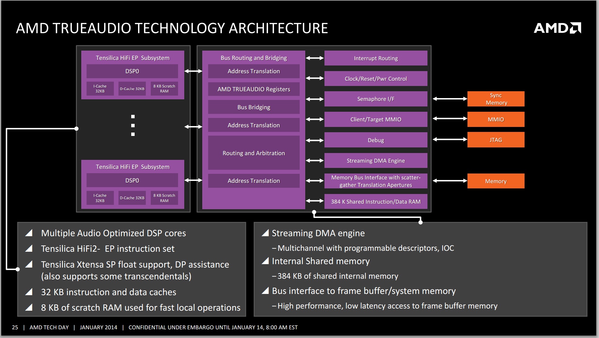
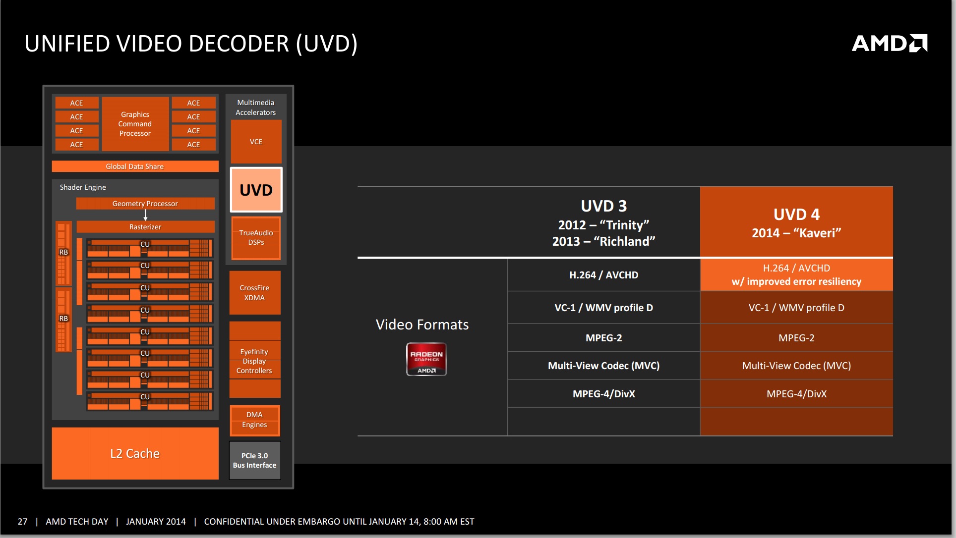
The feature set from Richland to Kaveri gets an update all around as well, with a fixed function TrueAudio DSP on the processor to offload complex audio tasks – AMD claims that reverb added to one audio sample for 3+ seconds can take >10% of one CPU core, so using the TrueAudio system allows game developers to enhance a full surround audio with effects, causing more accurate spatialization when upscaling to 7.1 or downscaling to stereo from 5.1. TrueAudio support unfortunately remains unused at launch, but Kaveri owners will be able to leverage the technology whenever games launch with it. Alongside TrueAudio, both the Unified Video Decoder (UVD) and the Video Coding Engine (VCE) are upgraded.
One of the prominent features of Kaveri we will be looking into is its HSA (Heterogenous System Architecture) – the tight coupling of CPU and GPU, extending all the way down to the programming model. Gone are the days when CPU and GPU cores have to be treated like independent inequals, with tons of data copies back and forth for both types of cores to cooperate on the same problem. With Kaveri, both CPU and GPU are treated as equal class citizens, capable of working on the same data in the same place in memory. It'll be a while before we see software take advantage of Kaveri's architecture, and it's frustrating that the first HSA APU couldn't have come with a different CPU, but make no mistake: this is a very big deal. The big push on AMD’s side is the development of tools for the major languages (OpenCL, Java, C++ and others) as well as libraries for APIs to do this automatically and with fewer lines of code.
Kaveri will support OpenCL 2.0, which should make it the first CPU/APU/SoC to carry that certification.
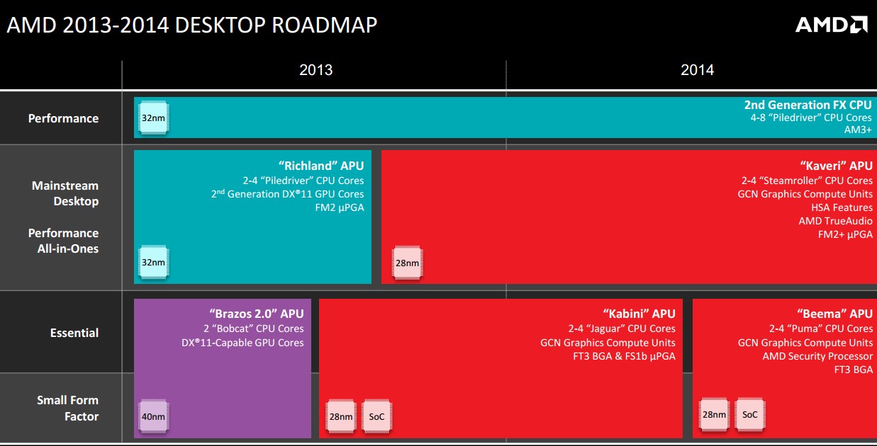
The Kaveri Lineup: Desktop Sweet Spot at 45W
For years now Intel has been targeting mobile first with its CPU architectures. More recently NVIDIA started doing the same with its GPUs (well, ultra-mobile first). With Haswell, Intel's architecture target shifted from 35 - 45W down to 10 - 20W, effectively making Ultrabook form factors the target for its CPU designs. Intel would then use voltage scaling to move the architecture up/down the stack, with Atom and Quark being used to go down to really low TDPs.
For AMD, Kaveri truly embraces the mobile first approach to design with a platform target of 35W. AMD is aiming higher up the stack than Intel did with Haswell, but it also has a lower end CPU architecture (Jaguar) that shoots a bit above Atom. I suspect eventually AMD will set its big architecture sights below 35W, but for now AMD plays the hand it was dealt. The Kaveri project was started 4 years ago and the Haswell platform retargeting was a mid-design shift (largely encouraged by Apple as far as I can tell), so it's not surprising to see Kaveri end up where it does. It's also worth pointing out that the notebook designs AMD primarily competes in are larger 35W machines anyways.
AMD's mobile roadmap states that we'll see Kaveri go all the way down to 15W (presumably in a 2-core/1-module configuration):
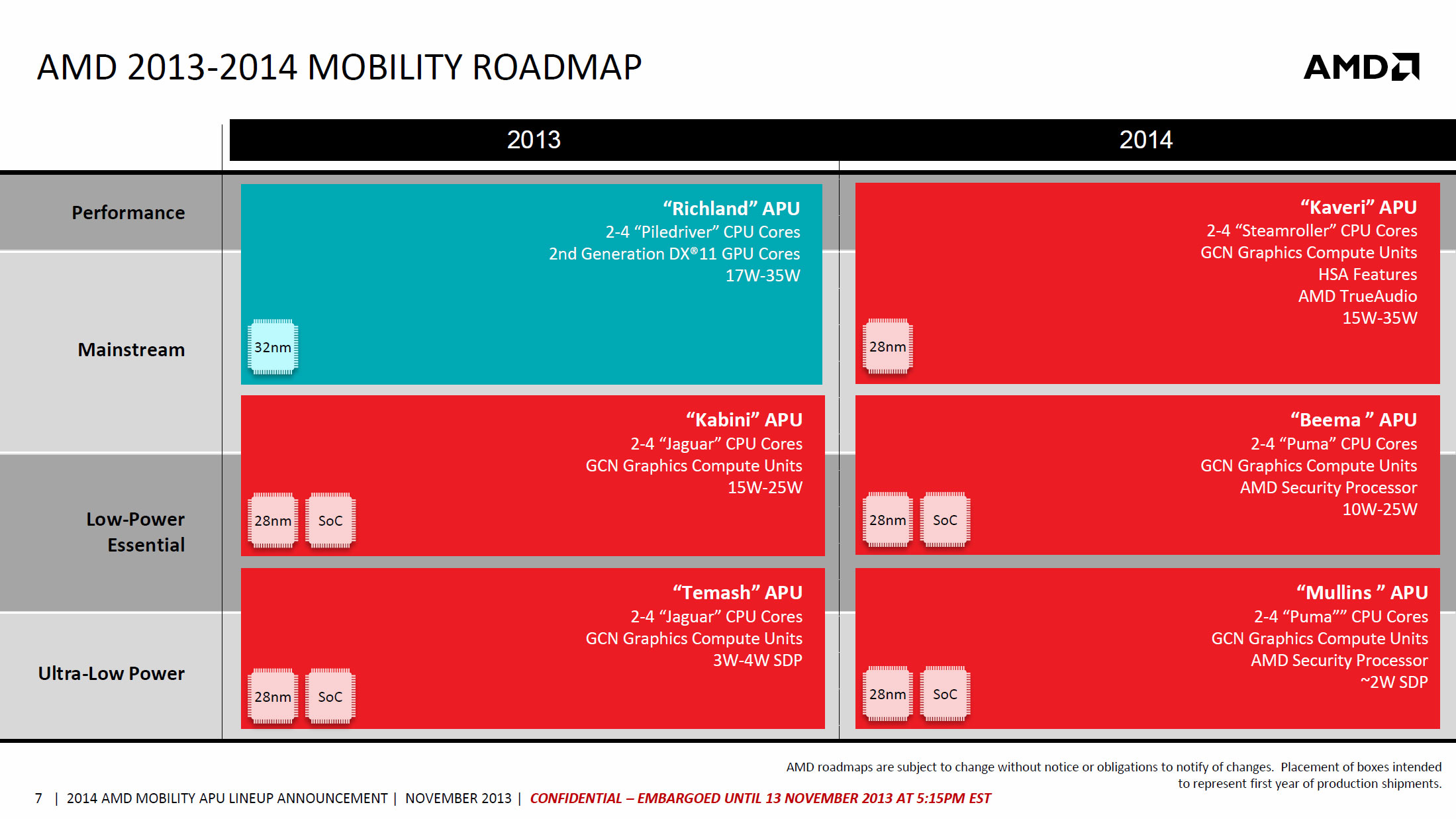
Kaveri mobile however appears to be a mid 2014 affair; what launches today are exclusively desktop parts. With an aggressive focus on power consumption, AMD's messaging around Kaveri is simply more performance at the same power.
Here are the Bulldozer based processors for each of AMD’s main desktop target segments: 45W, 65W and 95-100W:
| AMD 45W Bulldozer Based APUs | ||||
| Trinity | Richland | Kaveri | ||
| Model | - | A8-6500T | A8-6700T | A8-7600 |
| Core Name | - | Richland | Richland | Kaveri |
| Microarch | - | Piledriver | Piledriver | Steamroller |
| Socket | - | FM2 | FM2 | FM2+ |
| Modules/Cores | - | 2/4 | 2/4 | 2/4 |
| CPU Base Freq | - | 2100 | 2500 | 3100 |
| Max Turbo | - | 3100 | 3500 | 3300 |
| TDP | - | 45W | 45W | 45W |
| L1 Cache | - |
128KB I$ 64 KB D$ |
128 KB I$ 64 KB D$ |
192 KB I$ 64 KB D$ |
| L2 Cache | - | 2x2 MB | 2x2 MB | 2x2 MB |
| Graphics | - | HD 8550D | HD 8650D | R7 |
| GPU Cores | - | 256 | 284 | 384 |
| GPU Clock | - | 720 | 720 | 720 |
| Max DDR3 | - | 1866 | 1866 | 2133 |
| Current Price | - | N/A | N/A | $119 |
Actually, the 45W segment is almost a cop out here. AMD never released a 45W desktop edition of Trinity, and while it formally released a couple of 45W Richland APUs back in August, I literally have not seen them for sale in the regular markets (US, UK) that I check. After my initial Kaveri pre-launch information article, one reader got in touch and confirmed that a mid-sized Italian etailer was selling them and had some in stock, but the majority of the world can't seem to get a hold of them. For the purpose of this review, AMD was kind enough to source retail versions of both the A8-6500T and A8-6700T for comparison points to show how much the system has improved at that power bracket.
| AMD 65W Bulldozer Based APUs | ||||||
| Trinity | Richland | Kaveri | ||||
| Model | A6-5400K | A8-5500 | A10-5700 | A8-6500 | A10-6700 | A8-7600 |
| Core Name | Trinity | Trinity | Richland | Richland | Richland | Kaveri |
| Microarch | Piledriver | Piledriver | Piledriver | Piledriver | Piledriver | Steamroller |
| Socket | FM2 | FM2 | FM2 | FM2 | FM2 | FM2+ |
| Modules/Cores | 1/2 | 2/4 | 2/4 | 2/4 | 2/4 | 2/4 |
| CPU Base Freq | 3600 | 3200 | 3400 | 3500 | 3700 | 3300 |
| Max Turbo | 3800 | 3700 | 4000 | 4100 | 4300 | 3800 |
| TDP | 65W | 65W | 65W | 65W | 65W | 65W |
| L1 Cache |
64 KB I$ 32 KB D$ |
128 KB I$ 64 KB D$ |
128 KB I$ 64 KB D$ |
128 KB I$ 64 KB D$ |
128 KB I$ 64 KB D$ |
192 KB I$ 64 KB D$ |
| L2 Cache | 1 MB | 2 x 2 MB | 2 x 2 MB | 2 x 2 MB | 2 x 2 MB | 2x2 MB |
| Graphics | HD 7540D | HD 7560D | HD 7660D | HD 8570D | HD 8670D | R7 |
| GPU Cores | 192 | 256 | 384 | 256 | 384 | 384 |
| GPU Clock | 760 | 760 | 760 | 800 | 844 | 720 |
| Max DDR3 | 1866 | 1866 | 1866 | 1866 | 1866 | 2133 |
| Current Price | $60 | $99 | N/A | $119 | N/A | $119 |
By comparison, AMD has a history of making 65W CPUs. You may notice that the Kaveri model listed is the same model listed in the 45W table. This is one of the features of AMD’s new lineup – various models will have a configurable TDP range, and the A8-7600 will be one of them. By reducing the power by about a third, the user sacrifices a margin of CPU base speed and turbo speed, but no reduction in processor graphics speeds. At this point in time, the A8-7600 (45W/65W) is set for a Q1 release rather than a launch day release, and we have not received details of any further configurable TDP processors.
| AMD 95-100W Bulldozer Based APUs | ||||||
| Trinity | Richland | Kaveri | ||||
| Model | A8-5600K | A10-5800K | A8-6600K | A10-6800K | A10-7700K | A10-7850K |
| Core Name | Trinity | Trinity | Richland | Richland | Kaveri | Kaveri |
| Microarchi | Piledriver | Piledriver | Piledriver | Piledriver | Steamroller | Steamroller |
| Socket | FM2 | FM2 | FM2 | FM2 | FM2+ | FM2+ |
| Modules/Cores | 2/4 | 2/4 | 2/4 | 2/4 | 2/4 | 2/4 |
| CPU Base Freq | 3600 | 3800 | 3900 | 4100 | 3500 | 3700 |
| Max Turbo | 3900 | 4200 | 4200 | 4400 | 3800 | 4000 |
| TDP | 100W | 100W | 100W | 100W | 95W | 95W |
| L1 Cache |
128KB I$ 64KB D$ |
128KB I$ 64KB D$ |
128KB I$ 64KB D$ |
128KB I$ 64KB D$ |
192KB I$ 64KB D$ |
192KB I$ 64KB D$ |
| L2 Cache | 2 x 2 MB | 2 x 2 MB | 2 x 2 MB | 2 x 2 MB | 2 x 2 MB | 2 x 2 MB |
| Graphics | HD 7560D | HD 7660D | HD 8570D | HD 8670D | R7 | R7 |
| GPU Cores | 256 | 384 | 256 | 384 | 384 | 512 |
| GPU Clock | 760 | 800 | 844 | 844 | 720 | 720 |
| Max DDR3 | 1866 | 1866 | 1866 | 2133 | 2133 | 2133 |
| Current Price | $100 | $130 | $120 | $140 | $152 | $173 |
Here we see the 32nm SOI to bulk 28nm SHP shift manifesting itself in terms of max attainable frequency. Whereas the A10-6800K ran at 4.1/4.4GHz, the A10-7850K drops down to 3.7/4.0GHz (base/max turbo). TDP falls a bit as well, but it's very clear that anyone looking for the high end of AMD's CPU offerings to increase in performance won't find it with Kaveri. I suspect we'll eventually see an AMD return to the high-end, but that'll come once we're done with the Bulldozer family. For now, AMD has its sights set on the bulk of the mainstream market - and that's definitely not at 95/100W.
Kaveri Motherboard/Socket Compatibility
AMD’s socket and chipset situation with Kaveri also adjusts slightly, maintaining a small difference to Richland. The new APUs will only fit into an FM2+ socket motherboard, which differs from FM2 by two pins, and Richland/Trinity APUs will also fit into FM2+. However, Kaveri APUs will not fit into any older FM2 motherboards. On the chipset side, AMD is adding the A88X chipset to the Bulldozer chipset family, complementing A55, A75 and A85X. Similar to Trinity and Richland, the chipset is not a definitive indicator of the socket of the motherboard, except for A88X: A88X will only appear on FM2+ motherboards.
AMD has the workings of a potential platform changer, and certainly the programming paradigm change from ‘normal’ to HSA is one that is going to be at the forefront of AMD’s APU production for the foreseeable future.
Kaveri: Aiming for 1080p30 and Compute
The numerical differences between Kaveri and Richland are easy enough to rattle off – later in the review we will be discussing these in depth – but at a high level AMD is aiming for a middle ground between the desktop model (CPU + discrete graphics) and Apple’s Mac Pro dream (offloading compute onto different discrete graphics cards) by doing the dream on a single processor. At AMD’s Kaveri tech day the following graph was thrown in front of journalists worldwide:

With Intel now on board, processor graphics is a big deal. You can argue whether or not AMD should continue to use the acronym APU instead of SoC, but the fact remains that it's tough to buy a CPU without an integrated GPU.
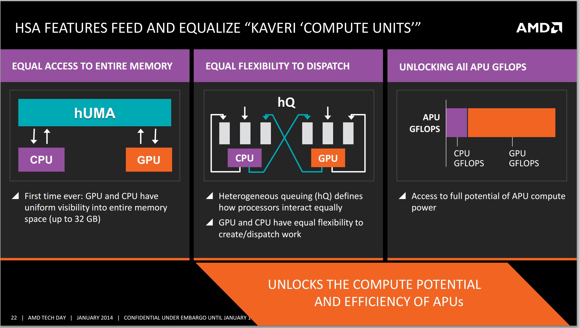
In the absence of vertical integration, software optimization always trails hardware availability. If you look at 2011 as the crossover year when APUs/SoCs took over the market, it's not much of a surprise that we haven't seen aggressive moves by software developers to truly leverage GPU compute. Part of the problem has been programming model, which AMD hopes to address with Kaveri and HSA. Kaveri enables a full heterogeneous unified memory architecture (hUMA), such that the integrated graphics topology can access the full breadth of memory that the CPU can, putting a 32GB enabled compute device into the hands of developers.
One of the complexities of compute is also time: getting the CPU and GPU to communicate to each other without HSA and hUMA requires an amount of overhead that is not trivial. For compute, this comes in the form of allowing the CPU and GPU to work on the same data set at the same time, effectively opening up all the compute to the same task without asynchronous calls to memory copies and expensive memory checks for coherency.
The issue AMD has with their HSA ecosystem is the need for developers to jump on board. The analogy oft cited is that on Day 1, iOS had very few apps, yet today has millions. Perhaps a small equivocation fallacy comes in here – Apple is able to manage their OS and system in its entirety, whereas AMD has to compete in the same space as non-HSA enabled products and lacks the control. Nevertheless, AMD is attempting to integrate programming tools for HSA (and OpenCL 2.0) as seamlessly as possible to all modern platforms via a HSA Instruction Layer (HSAIL). The goal is for programming languages like Java, C++ and C++ AMP, as well as common acceleration API libraries and toolkits to provide these features at little or no coding cost. This is something our resident compute guru Rahul will be looking at in further detail later on in the review.
On the gaming side, 30 FPS has been a goal for AMD’s integrated graphics solutions for a couple of generations now.

Arguably we could say that any game should be able to do 30 FPS if we turn down the settings far enough, but AMD has put at least one restriction on that: resolution. 1080p is a lofty goal to hold at 30 FPS with some of the more challenging titles of today. In our testing in this review, it was clear that users had a choice – start with a high resolution and turn the settings down, or keep the settings on medium-high and adjust the resolution. Games like BF4 and Crysis 3 are going to tax any graphics card, especially when additional DirectX 11 features come in to play (ambient occlusion, depth of field, global illumination, and bilateral filtering are some that AMD mention).
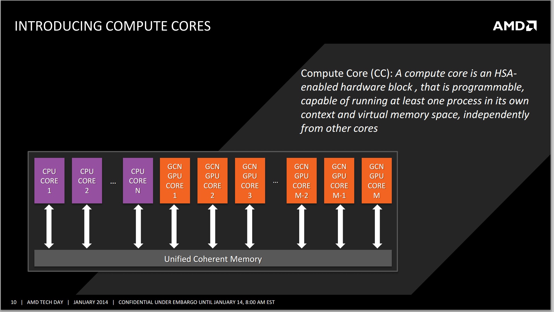
Kaveri and Counting Cores
With the move towards highly integrated SoCs we've seen a variety of approaches to core counts. Apple, Intel and Qualcomm still count CPU cores when advertising an SoC. For Apple and Qualcomm that's partially because neither company is particularly fond of disclosing the configuration of their GPUs. More recently, NVIDIA took the somewhat insane stance of counting GPU CUDA cores on its Tegra K1 SoC. Motorola on the other hand opted for the bizarre choice of aggregating CPU, GPU and off-die companion processors with the X8 platform in its Moto X smartphone. Eventually we will have to find a way to characterize these highly integrated SoCs, particularly when the majority of applications actually depend on/leverage both CPU and GPU cores.
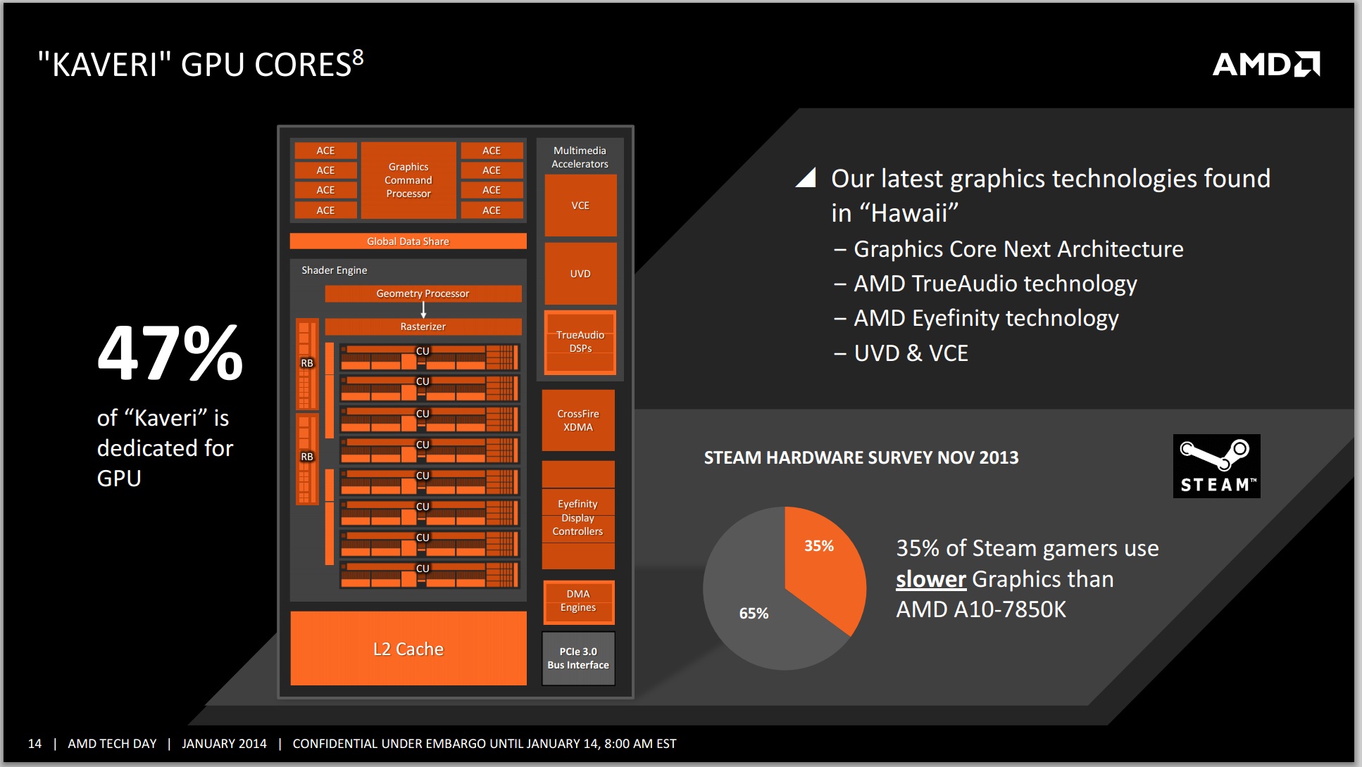
AMD finds itself in a unique position with Kaveri where it has a truly unified CPU/GPU architecture and needs to establish a new nomenclature for use in the future. With 47% of the Kaveri die dedicated for GPU use, and an architecture that treats both CPU and GPU as equals, I can understand AMD's desire to talk about the number of total cores on the APU.
AMD settled on the term "Compute Core", which can refer to either an x86 (or maybe eventually ARM) CPU core or a GCN compute unit. The breakdown is as follows:
- Each thread on a CPU is a Compute Core
- Each Compute Unit on the IGP is a Compute Core
- Total Compute Cores = CPU Compute Cores + IGP Compute Cores
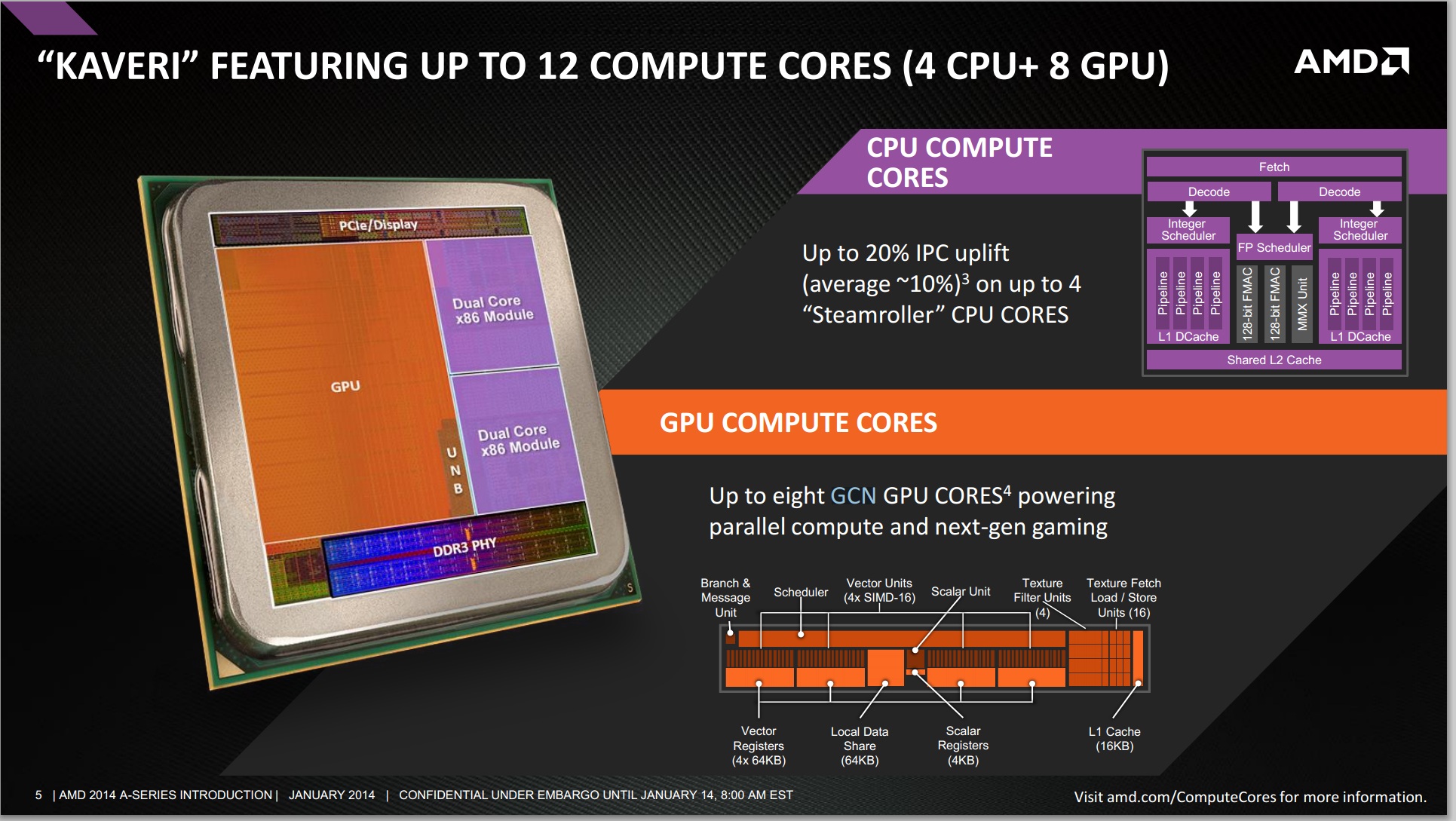
This means that the high end SKU, the A10-7850K will have a total of 12 compute cores: four from the CPU (two Steamroller modules supporting four threads) and eight from the IGP (due to eight compute units from the R7 graphics).
There are some qualifications to be made on this front. Technically, AMD is correct – each compute unit in the IGP and each thread on the CPU can run separate code. The Hawaii GCN architecture can spawn as many kernels as compute units, whereas a couple of generations ago we were restricted to one compute kernel on the GPU at once (merely with blocks of work being split across the CUs). However, clearly these 12 compute units are not equivalent: a programmer will still have to write code for the CPU and GPU specifically in order to use all the processing power available.
Whenever AMD (or partners) are to promote the new APUs, AMD tells us clearly that two sets of numbers should be quoted in reference to the Compute Cores – the total, and the breakdown of CPU/GPU on the APU. Thus this would mean that the A10-7850K APU would be marketed at a “12 Compute Core” device, with “(4 CPU + 8 GPU)” following immediately after. I applaud AMD's decision to not obfuscate the internal configuration of its APUs. This approach seems to be the most sensible if it wants to tout the total processing power of the APU as well as tell those users who understand a bit more what the actual configuration of the SoC is. The biggest issue is how to address the users who automatically assume that more cores == better. The root of this problem is very similar to the old PR-rating debates of the Athlon XP. Explaining to end users the intracacies of CPU/GPU programming is really no different than explaining why IPC * frequency matters more than absolute frequency.
When a programmer obtains an APU, the OpenCL profiler should locate the eight compute units of the GPU and display that to the user for offloading compute purposes; at the same time it is up to the programmer to leverage the threads as appropriately as possible, even with AMD’s 3rd generation Bulldozer modules implementing a dual-INT + single-FP solution.
At launch, AMD will offer the following configurations:
- A10-7850K: 12 Compute Cores (4 CPU + 8 GPU)
- A10-7700K: 10 Compute Cores (4 CPU + 6 GPU)
- A8-7600: 10 Compute Cores (4 CPU + 6 GPU)
The problem with distilling the processing power of the APU into a number of compute cores is primarily on the CPU side. AMD will be keeping the GPU at approximately the same clock (720 MHz for these three) but the CPU frequency will differ greatly, especially with the A8-7600 which has configurable TDP and when in 45W mode will operate 300-400 MHz less.
Steamroller Architecture Redux
We've already documented much of what Steamroller brings to the table based on AMD's Hot Chips presentation last year, but I'll offer a quick recap here.
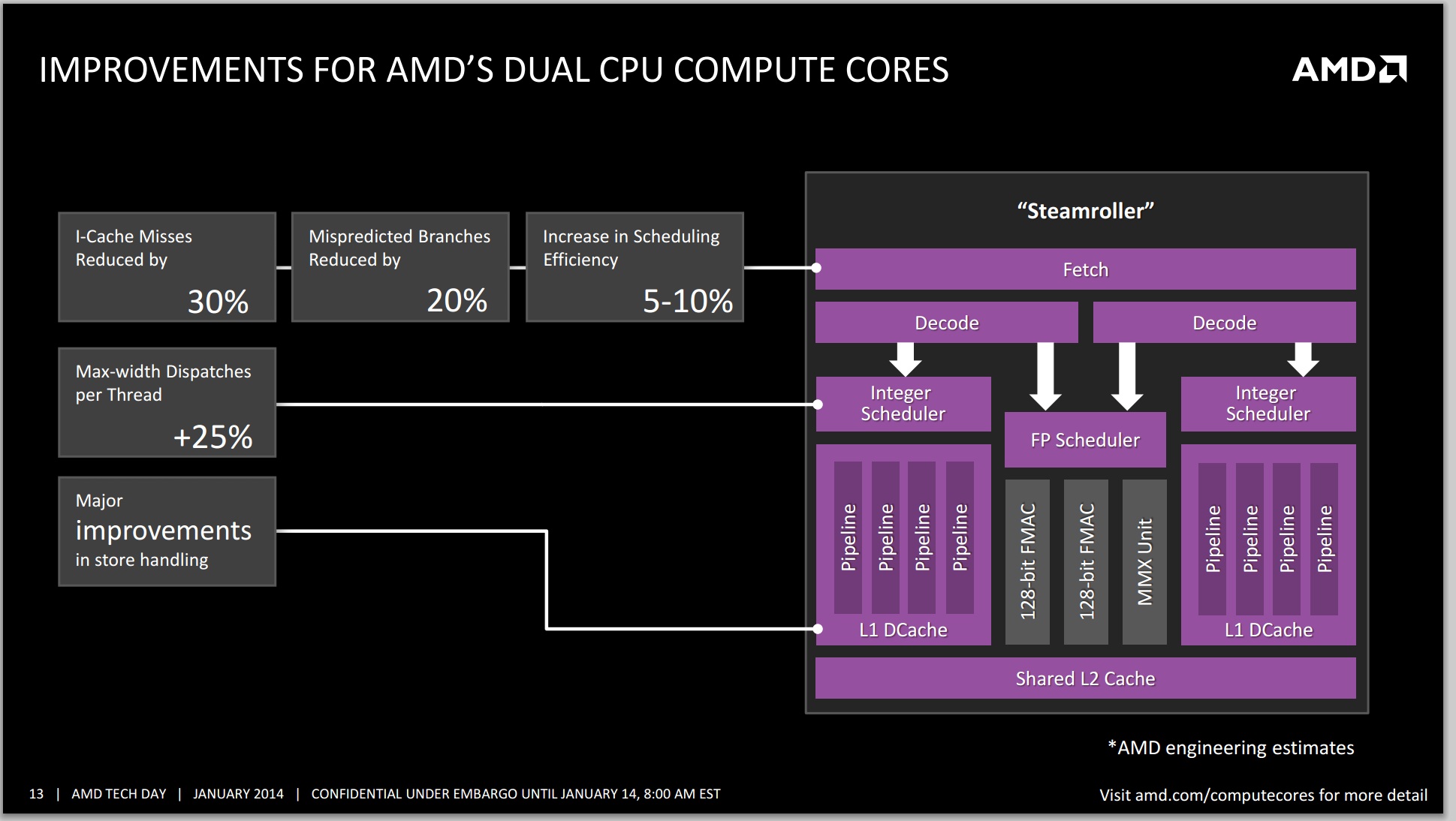
Steamroller brings forward AMD's Bulldozer architecture, largely unchanged. We're still talking about a dual-core module featuring two independent integer execution cores with a single shared floating point execution core capable of executing instructions from two threads in parallel. A single module still appears as two cores/threads to the OS.
In Bulldozer and Piledriver, each integer core had its own independent scheduler but the two cores shared a single fetch and decode unit. Instructions would come in and decodeded operations would be fed to each integer pipe on alternating clock cycles. In Steamroller the decode hardware is duplicated in each module, so now each integer core gets its own decode unit. The two decode units are shared by the one FP unit.
L1 instruction caches increase in size from 64KB to 96KB per module, which AMD claims reduces misses by up to 30%. There's an updated branch predictor which is responsible for reducing mispredicted branches by up to 20%. Both integer and FP register files grow in size as well as an increase in the size of the scheduling window, a combination of which increases the number of dispatches per thread by up to 25%.
There are huge improvements on the store side. Steamroller can now issue up to 2 stores at the same time compared to 1 in Bulldozer/Piledriver. The load/store queue sizes go up by around 20% as well. It's remarkable just how much low hanging fruit there was in the Bulldozer design.
GCN in an APU
The integrated graphics solution on Trinity/Richland launched with a Cayman-derived VLIW4 architecture, which unfortunately came just shortly after desktop side of the equation finished moving from VLIW5/VLIW4 to GCN. Having a product stack with largely different GPU architectures doesn't help anyone, particularly on the developer front. Looking forward, sticking with GCN was the appropriate thing to do, as now Kaveri is using GCN, the same architecture found in AMD’s high end R9-290X GPU, based on the Hawaii platform.
This enabled AMD to add in all the features they currently have on Hawaii with little to no effort – the TrueAudio DSP, the upgraded Video Coding Engine and Unified Video Decoder are such examples. Whether or not AMD decides to develop an APU with more than 8 GCN CUs is another matter. This is a point we've brought up with AMD internally and one that I'm curious about - do any AnandTech readers have an interest in an even higher end APU with substantially more graphics horsepower? Memory bandwidth obviously becomes an issue, but the real question is how valuable an Xbox One/PS4-like APU would be to the community.
Llano, Trinity and Kaveri Die: Compared
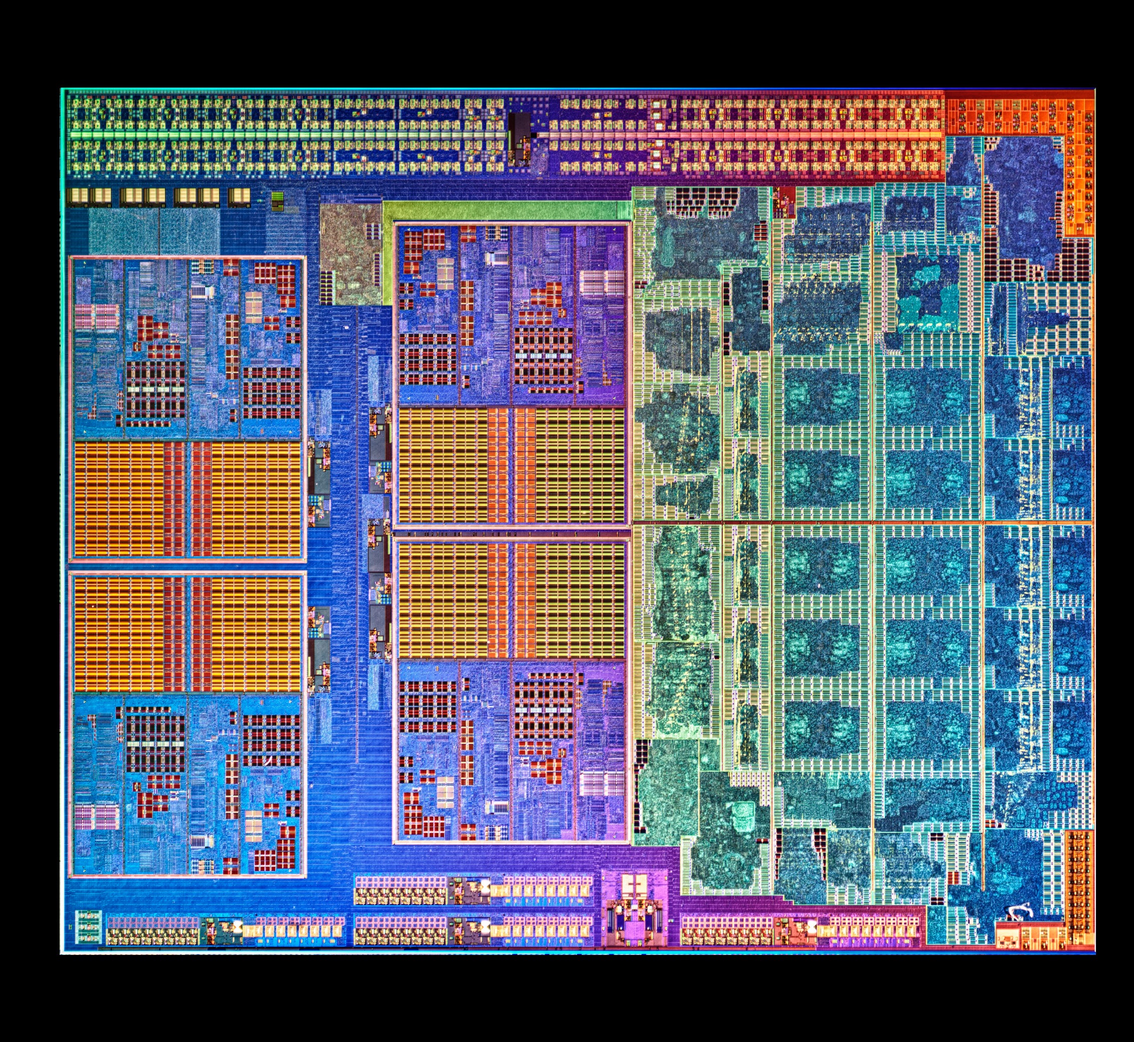
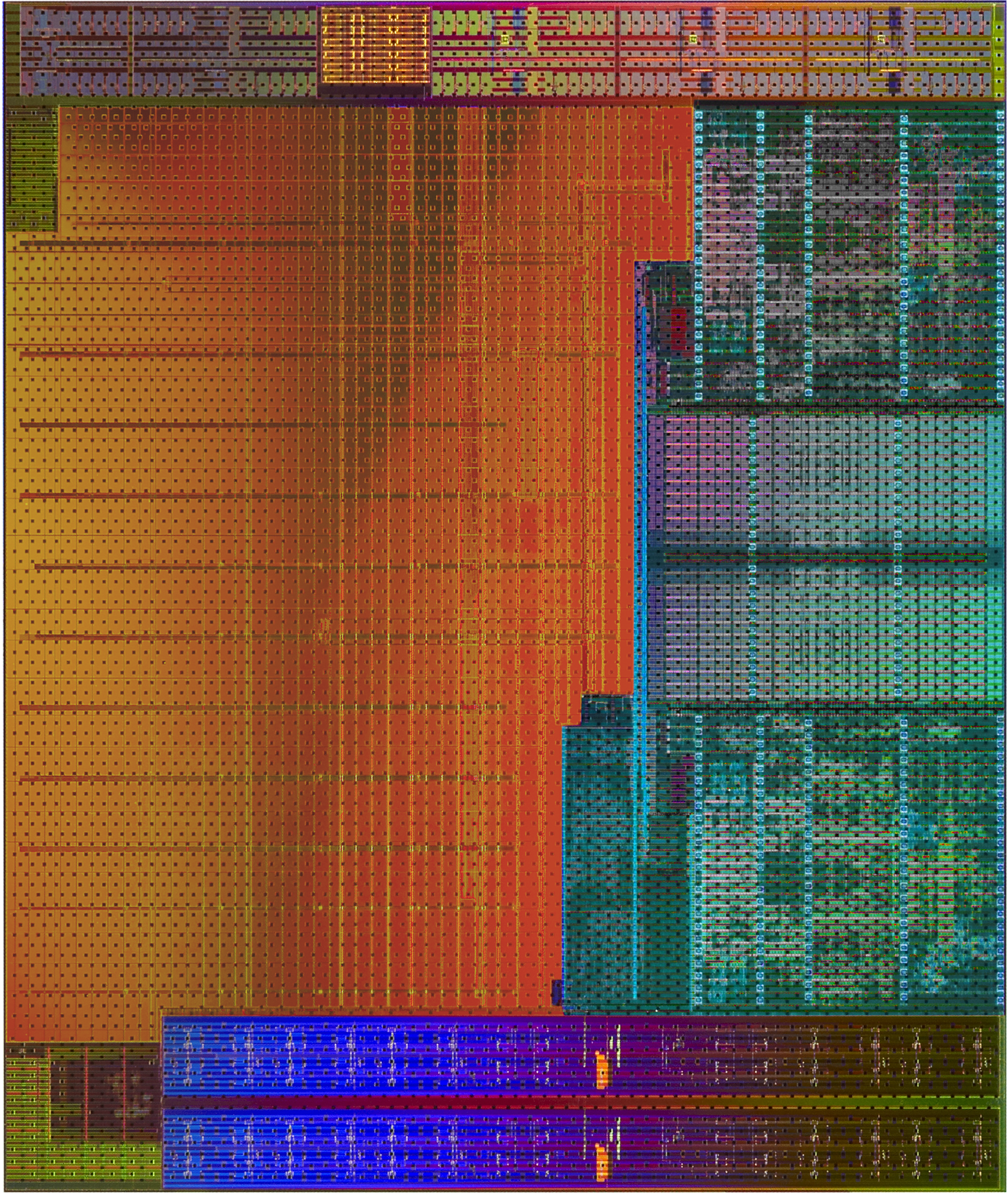
AMD sent along a high res shot of Kaveri's die. Armed with the same from the previous two generations, we can get a decent idea of the progression of AMD's APUs:
Llano, K10 Quad Core

Trinity and Richland Die, with two Piledriver modules and processor graphics
Kaveri, two modules and processor graphics
Moving from Llano to Trinity, we have the reduction from a fully-fledged quad core system to the dual module layout AMD is keeping with its APU range. Moving from Richland to Kaveri is actually a bigger step than one might imagine:
| AMD APU Details | ||||
| Core Name | Llano | Trinity | Richland | Kaveri |
| Microarch | K10 | Piledriver | Piledriver | Steamroller |
| CPU Example | A8-3850 | A10-5800K | A10-6800K | A10-7850K |
| Threads | 4 | 4 | 4 | 4 |
| Cores | 4 | 2 | 2 | 2 |
| GPU | HD 6550 | HD 7660D | HD 8670D | R7 |
| GPU Arch | VLIW5 | VLIW4 | VLIW4 | GCN 1.1 |
| GPU Cores | 400 | 384 | 384 | 512 |
| Die size / mm2 | 228 | 246 | 246 | 245 |
| Transistors | 1.178 B | 1.303 B | 1.303 B | 2.41 B |
| Power | 100W | 100W | 100W | 95W |
| CPU MHz | 2900 | 3800 | 4100 | 3700 |
| CPU Turbo | N/A | 4200 | 4400 | 4000 |
| L1 Cache |
256KB C$ 256KB D$ |
128KB C$ 64KB D$ |
128KB C$ 64KB D$ |
192KB C$ 64KB D$ |
| L2 Cache | 4 x 1MB | 2 x 2 MB | 2 x 2 MB | 2 x 2 MB |
| Node | 32nm SOI | 32nm SOI | 32nm SOI | 28nm SHP |
| Memory | DDR-1866 | DDR-1866 | DDR-2133 | DDR-2133 |
Looking back at Llano and Trinity/Richland, it's very clear that AMD's APUs on GF's 32nm SOI process had a real issue with transistor density. The table below attempts to put everything in perspective but keep in mind that, outside of Intel, no one does a good job of documenting how they are counting (estimating) transistors. My only hope is AMD's transistor counting methods are consistent across CPU and GPU, although that alone may be wishful thinking:
| Transistor Density Comparison | ||||||||
| Manufacturing Process | Transistor Count | Die Size | Transistors per mm2 | |||||
| AMD Kaveri | GF 28nm SHP | 2.41B | 245 mm2 | 9.837M | ||||
| AMD Richland | GF 32nm SOI | 1.30B | 246 mm2 | 5.285M | ||||
| AMD Llano | GF 32nm SOI | 1.178B | 228 mm2 | 5.166M | ||||
| AMD Bonaire (R7 260X) | TSMC 28nm | 2.08B | 160 mm2 | 13.000M | ||||
| AMD Pitcairn (R7 270/270X) | TSMC 28nm | 2.80B | 212 mm2 | 13.209M | ||||
| AMD Vishera (FX-8350) | GF 32nm SOI | 1.2B | 315 mm2 | 3.810M | ||||
| Intel Haswell 4C (GT2) | Intel 22nm | 1.40B | 177 mm2 | 7.910M | ||||
| NVIDIA GK106 (GTX 660) | TSMC 28nm | 2.54B | 214 mm2 | 11.869M | ||||
If AMD is indeed counting the same way across APUs/GPUs, the move to Kaveri doesn't look all that extreme but rather a good point in between previous APUs and other AMD GCN GPUs. Compared to standalone CPU architectures from AMD, it's clear that the APUs are far more dense thanks to big portions of their die being occupied by a GPU.
TrueAudio
As part of the Kaveri package, AMD is also focusing on adding and updating their fixed function units / accelerators. Due to the jump on the GPU side to GCN we now have the TrueAudio DSP to allow developers to increase the audio capabilities in game, and both the Video Codec Engine (VCE) and Unified Video Decoder (UVD) have been updated.
All the major GPU manufacturers on the desktop side (AMD, NVIDIA, Intel) are pushing new technologies to help improve the experience of owning one of their products. There are clearly many ways to approach this – gaming, compute, content consumption, low power, high performance and so on. This is why we have seen feature like FreeSync, G-Sync, QuickSync, OpenCL adoption and the like become part of the fold in terms of these graphics solutions.
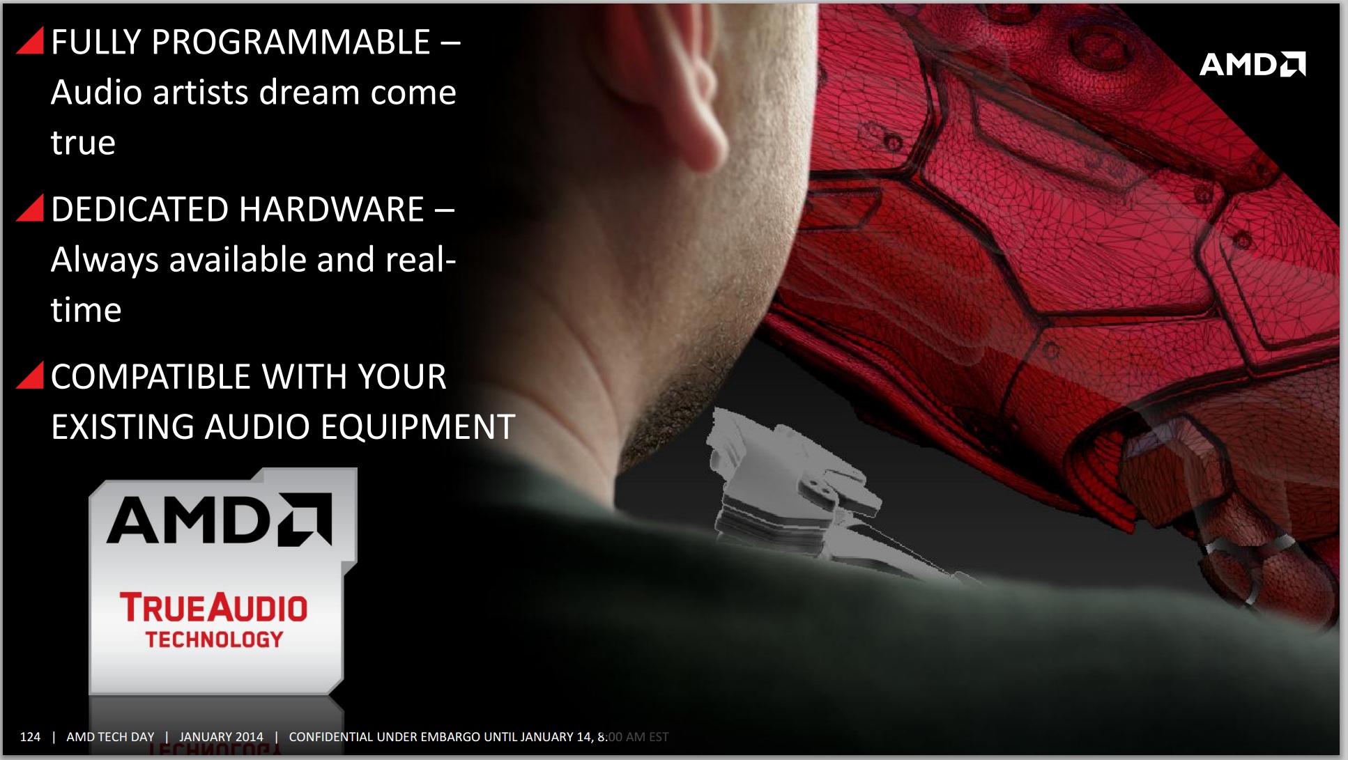
AMD’s new feature is TrueAudio - a fully programmable dedicated hardware element to offload audio tasks to.
The main problem with developing new tools comes down to whether they should be implemented in a general fashion or with a dedicated element. This comes down to the distinction of having a CPU or an ASIC do the work – if the type of work is specific and never changes, then an ASIC makes sense due to its small size, low power overhead and high throughput. A CPU wins out when the work is not clearly defined and it might change, so it opens up the realm of flexibility in exchange for performance per watt.
CPUs are now significantly powerful that a range of audio based techniques are available to them and the algorithms are optimized. The only limitation in this regard is the imagination of the developer or audio artist, which actually becomes part of the problem. When implementing an audio filter on the fly to a video game, the processing via the CPU can be overly taxing, especially when the effect is persistent over a long time. The example AMD gave in their press slide deck is one of adding reverb to an audio sample. The longer the reverb, the bigger the draw on CPU resources:
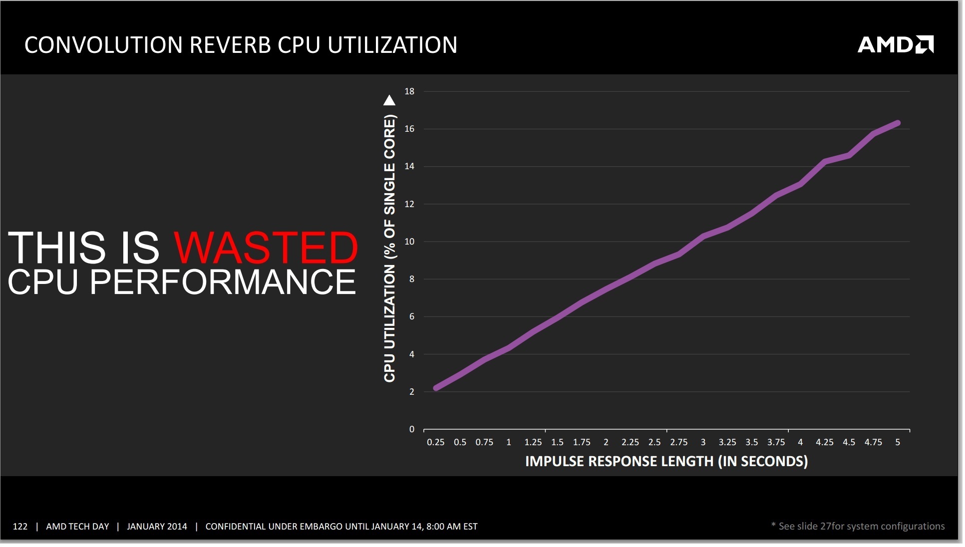
AMD cites this CPU usage as the effect of one filter on one audio sample. Imagine being in a firefight situation in a video game, whereby there are many people running around with multiple gunshots, splatter audio and explosions occurring. Implementing effects on all, and then transposing audio location to the position of the character is actually computationally expensive, all for the sake of realism. This is where the TrueAudio unit comes into play – the purpose is to offload all of this onto a dedicated bit of silicon that has the pathways built in for quicker calculations.
TrueAudio is also implemented on AMD's latest-generation R9 260 and R9 290 video cards – basically anything at least GCN 1.1 and up. Meanwhile we also know that the PS4’s audio DSP is based on TrueAudio, though given the insular nature of console development it's not clear whether the APIs are also the same on both platforms. AMD for their part is working with major audio middleware plugins (wwise, Bink) in order to help develop the TrueAudio ecosystem, so even in the case where the APIs are dissimilar, middleware developers can abstract that and focus on the similarities in the hardware underneath.
As is usually the case for these additional hardware features, games will need to specifically be coded to use TrueAudio, and as such the benefits of TrueAudio will be game specific. At the same time there are not any games currently on the market that can take advantage of the feature, so the hardware is arriving before there is software ready to use it. The first three games on AMD's list that will support TrueAudio are Murdered: Soul Suspect, Thief, and Lichdom. Much like FreeSync, I expect the proof is in the pudding and we will have to wait to see how it can affect the immersion factor of these titles.


Unified Video Decoder and Video Codec Engine
I wanted to include some talk about the UVD and VCE with Kaveri as both are updated – we get UVD 4, an update to error resiliency for H.264, and VCE 2, as shown below:
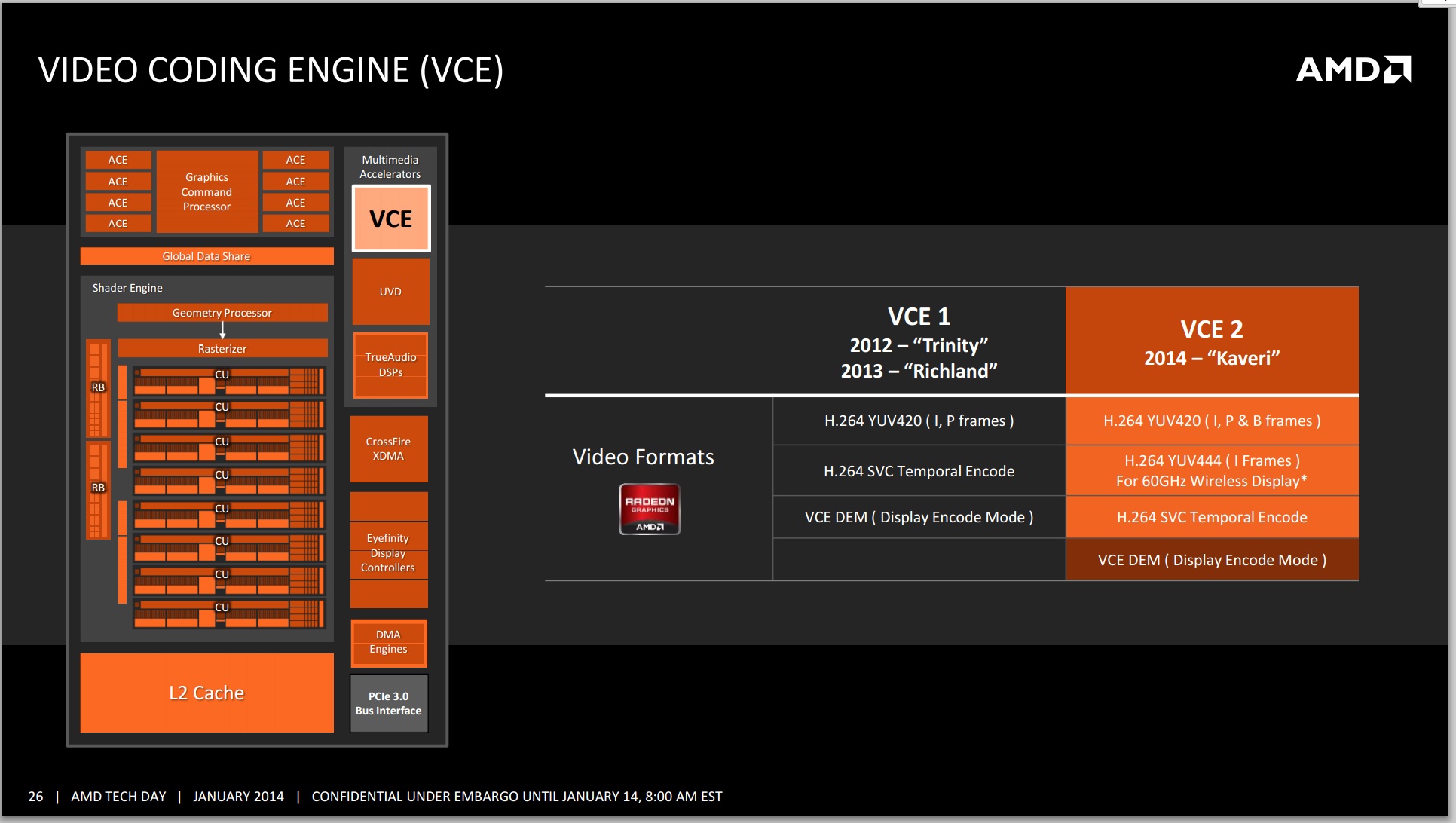
Of the two blocks, the improved VCE has the more interesting improvements to discuss. With the addition of support for B frames in H.264 encoding, the resulting ability to do backwards frame prediction should help improve the resulting image quality from VCE and/or reduce the required bitrates for any given quality level. Meanwhile the addition of support for the higher quality YUV444 color space in the H.264 encoder should help with the compression of primarily linear lineart/text, which in turn is important for the clarity of wireless displays.
A Deep Dive on HSA
For our look into Heterogeneous System Architecture (HSA), Heterogeneous Unified Memory Architecture (hUMA) and Heterogeneous Queuing (hQ), our resident compute expert Rahul Garg steps up to the plate to discuss the implication, implementation and application of such concepts:
GPUs are designed for solving highly parallel problems - for example, operations on matrices are highly parallel and usually well-suited to GPUs. However, not every parallel problem is suitable for GPU compute. Currently using GPUs for most problems requires copying data between the CPU and GPU - for discrete GPUs, typically an application will copy data from system RAM to the GPU memory over the PCIe bus, do some computation and then send the results back over the PCIe bus when the computation is complete. For example, matrix addition is a highly parallel operation that has been well documented and optimized for parallelism on CPUs and GPUs alike, but depending on the structure of the rest of the application, may not be suitable for GPU acceleration if the copy demands over the PCIe bus are strenuous to the overall speed of the application. In this example, the data transfer time alone will often be more expensive than doing the matrix addition on the CPU. The data copy between the CPU and the GPU also introduces complexity in software development.
There are two reasons for the necessity of fast data transfer today. First, GPU compute currently usually implies using a discrete GPU attached to the system over the PCIe bus. Discrete GPUs have their own onboard RAM, usually in the range of 1GB to 4GB or up to 12GB on some recent server-oriented cards. The onboard RAM may have a high bandwidth (say GDDR5) in order to hide latency between thread context switching, sometimes cited as the holy-grail in high memory access compute tasks. In this setup, even if we assume that the GPU could read/write data in system RAM over PCIe bus, it is often more efficient to just transfer all relevant data to this onboard RAM once only, and let the compute kernels read/write data from the onboard GPU RAM instead of attempting to read/write data slowly over PCIe. The second reason for data copies is that the CPU and the GPU have distinct address spaces. Before HSA, they could not make sense of each other's address spaces. Even integrated GPUs, which do physically share the same memory, did not have the necessary bookkeeping machinery necessary for a unified address space. HSA addresses this second scenario.
People have been trying many techniques to avoid the data transfer overhead. For example, you can try to do data transfers in parallel with some other computation on the CPU so that computation and communication overlap. In some cases, the CPU can be bypassed altogether, for example by transferring some file data from a PCIe SSD directly to the GPU using GPUDirect. However, such techniques are not always applicable and require a lot of effort from the programmer. Ultimately, true shared memory between CPU and GPU is the way to go for many problems though discrete GPUs with their onboard high-bandwidth RAM will shine on many other problems despite the data-copy overhead.
Unified memory: State of the art before HSA
The terms "shared memory" or "unified memory" are actually thrown about quite frequently in the industry and can mean different things in different contexts. We examine the current state of art across platform distributors:
NVIDIA has introduced "unified memory" in CUDA. However, on current chips, it is a software-based solution that is more of a convenience for software developers and hidden behind APIs for ease of use. The price of data transfer still needs to be paid in terms of performance, and NVIDIA's tools merely hide some of the software complexity. However, NVIDIA is expected to offer true shared memory in the Maxwell generation, which will likely be integrated into the successor of Tegra K1 in 2015 or 2016.
AMD: AMD touts "zero copy" on Llano and Trinity for OpenCL programs. However, in most cases, this only provides a fast way to copy data from CPU to GPU and the ability to read data back from GPU in some limited cases. In practice, the zero copy feature has limited uses due to various constraints such as high initialization cost. For most use cases, you will end up copying data between CPU and GPU.
Intel: Intel provides some support for shared memory today on the Gen7 graphics in Ivy Bridge and Haswell exposed through OpenCL and DirectX. Intel's CPU/GPU integration is actually more impressive than Llano or Trinity from the perspective of memory sharing. However, sharing is still limited to some simple cases as it is missing pointer sharing, demand-based paging and true coherence offered in HSA and thus the integration is far behind Kaveri. I am expecting better support in Broadwell and Skylake. Intel's socketed Knights Landing (future Xeon Phi) product may also enable heterogeneous systems where both CPU and accelerator access the same memory, which might be the way forward for discrete GPUs as well (if possible).
Others: Companies like ARM, Imagination Technologies, Samsung and Qualcomm are also HSA Foundation members and probably working on similar solutions. Mali T600 and T700 GPUs expose some ability of sharing GPU buffers between CPU and GPU through OpenCL 1.1. However, I don't think we will see a full HSA stack from vendors other than AMD in the near future.
As of today, HSA model implemented in Kaveri is the most advanced CPU-GPU integration yet and offers the most complete solution of the bunch.
hUMA: Unified Memory in HSA
Now we examine the unified memory capabilities provided in HSA. The main benefits of having a heterogeneous unified memory architecture in HSA boil down to the addressable memory space. By reducing the cost of having the CPU and GPU access the same data, compute can be improved or offloaded without worrying about the expense of such an operation.
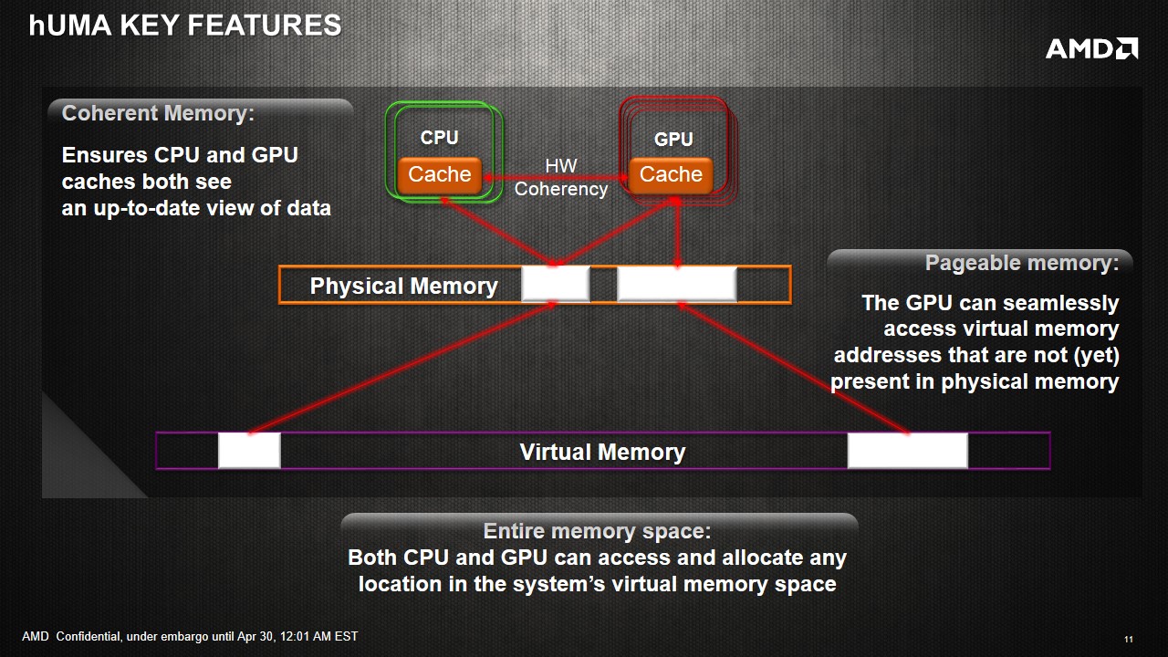
Eliminating CPU-GPU data copies: GPU can now access the entire CPU address space without any copies. Consider our matrix addition example again. In an HSA system, the copy of input data to GPU and copy of results back to CPU can be eliminated.
Access to entire address space: In addition to the performance benefit of eliminating copies, the GPU is also no longer limited to the onboard RAM as is usually the case with discrete GPUs. Even top-end discrete cards top out at about 12GB of onboard RAM currently while a CPU had the advantage of having access to potentially a much larger pool of memory. In many cases, such as scientific simulations, this would mean that the GPU can now work on much larger datasets without any special effort on the part of the programmer to somehow fit the data into GPU's limited address space. Kaveri will have access up to 32GB DDR3 memory, whereby the limiting factor is more the lack of 16GB unregistered non-ECC memory sticks on the market. The latency between the APU and the DRAM still exists however, meaning that a large L3 or eDRAM in the future might improve the scenario, especially in memory bandwidth limited scenarios and pre-empting data fetching.
Unified addressing in hardware: This is the big new piece in Kaveri and HSA that is not offered by any other system currently. Application programs allocate memory in a virtual CPU memory space and the OS maintains a mapping between virtual and physical addresses. When the CPU encounters a load instruction, it converts the virtual address to physical address and may need the assistance of the OS. The GPU also has its own virtual address space and previously did not understand anything about the CPU's address space. In the previous generation of unified memory systems like Ivy Bridge, the application had to ask the GPU driver to allocate a GPU page table for a given range of CPU virtual addresses. This worked for simple data structures like arrays, but did not work for more complicated structures. Initialization of the GPU page table also created some additional performance overhead.
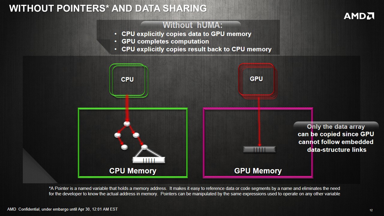
In HSA, the GPU can directly load/store from CPU virtual address space. Thus, the application can directly pass CPU pointers enabling a much broader class of applications to take advantage of GPU. For example, sharing linked-lists and other pointer-based data structures is now possible without complicated hijinks from the application. There is also no driver overhead in sharing pointers, and thus provides better efficiency.
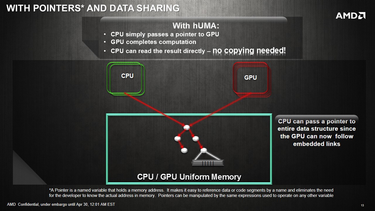
With this solution, the CPU and the GPU can access the same data set at the same time, and also perform work on the data set together. This enables developers to program for high utilization scenarios, and gets around AMD’s calculations of 800+ GFLOPs coming from a single Kaveri APU. With up to 12 compute cores, despite having to use CPU and GPU compute cores differently and with different kernels, they can at least all access the same data with zero overhead. It will still be up to the developer to manage locks and thread fences to ensure data coherency.
Demand-driven paging: We overlooked one detail in the previous discussion. Converting virtual addresses to physical addresses is a non-trivial task - the page containing the desired physical location may not actually be in memory and may need to loaded from, say, the disk and requires OS intervention. This is called demand-driven paging. GPUs prior to Kaveri did not implement demand-driven paging. Instead, the application had to know in advance what range of memory addresses it was going to access and map those to a GPU buffer object. The GPU driver then locked the corresponding pages in memory. However, in many cases the application programmer may not know the access pattern beforehand. Pointer-based data structures like linked lists, where the nodes may be pointing to anywhere in memory, were difficult to deal with. Demand-driven paging, together with unified addressing, allows sharing of arbitrary data structures between CPU and GPU and thus opens the door to GPU acceleration of many more applications.
CPU-GPU coherence: So far we have discussed how the GPU can read/write from the CPU address space without any data copies. However, that is not the full story. CPU and the GPU may want to work together on a given problem. For some types of problems, it is critical that the CPU/GPU be able to see each other's writes during the computation. This is non-trivial because of issues such as caches. HSA memory model provides optional coherence between the CPU and the GPU through what is called acquire-release type memory instructions. However, this coherence comes at a performance cost and thus HSA provides mechanisms for the programmer to express when CPU/GPU coherence is not required. Apart from coherent memory instructions, HSA also provides atomic instructions that allow the CPU to GPU to read/write atomically from a given memory location. These ‘platform atomics’ are designed to do as regular atomics, i.e. provide a read-modify-write operation in a single instruction without developing custom fences or locks around the data element or data set.
HSAIL: Portable Pseudo-ISA for Heterogeneous Compute
The HSA Foundation wants that the same heterogeneous compute applications run on all HSA-enabled systems. Thus, they needed to standardize the software interface supported by any HSA-enabled system. HSA foundation wanted a low-level API to the hardware that can be targeted by compilers of different languages. Typically compilers target the instruction-set of a processor. However, given the diversity of hardware being targeted by HSA (CPUs, GPUs, DSPs and more), standardizing on an instruction-set was not possible. Instead, HSA Foundation has standardized on a pseudo-instruction set called HSAIL. HSAIL stands for HSA Intermediate Language. The idea is that the compiler for a high-level language (like OpenCL, C++ AMP or Java) will generate HSAIL and the HSA driver will generate the actual binary code using just-in-time compilation. The idea of a pseudo-ISA has been used in many previous portable technologies such as Java bytecode and the Direct3D bytecode. HSAIL is low-level enough to expose many details of the hardware and has been carefully designed such that the conversion from HSAIL to binary code can be very fast.
In terms of competition, Nvidia provides PTX which has similar goals to HSAIL in terms of providing a pseudo instruction set target for compilers. PTX is only meant for Nvidia systems, though some research projects do provide alternate backends such as x86 CPUs. HSAIL will be portable to any GPU, CPU or DSP that implements HSA APIs.
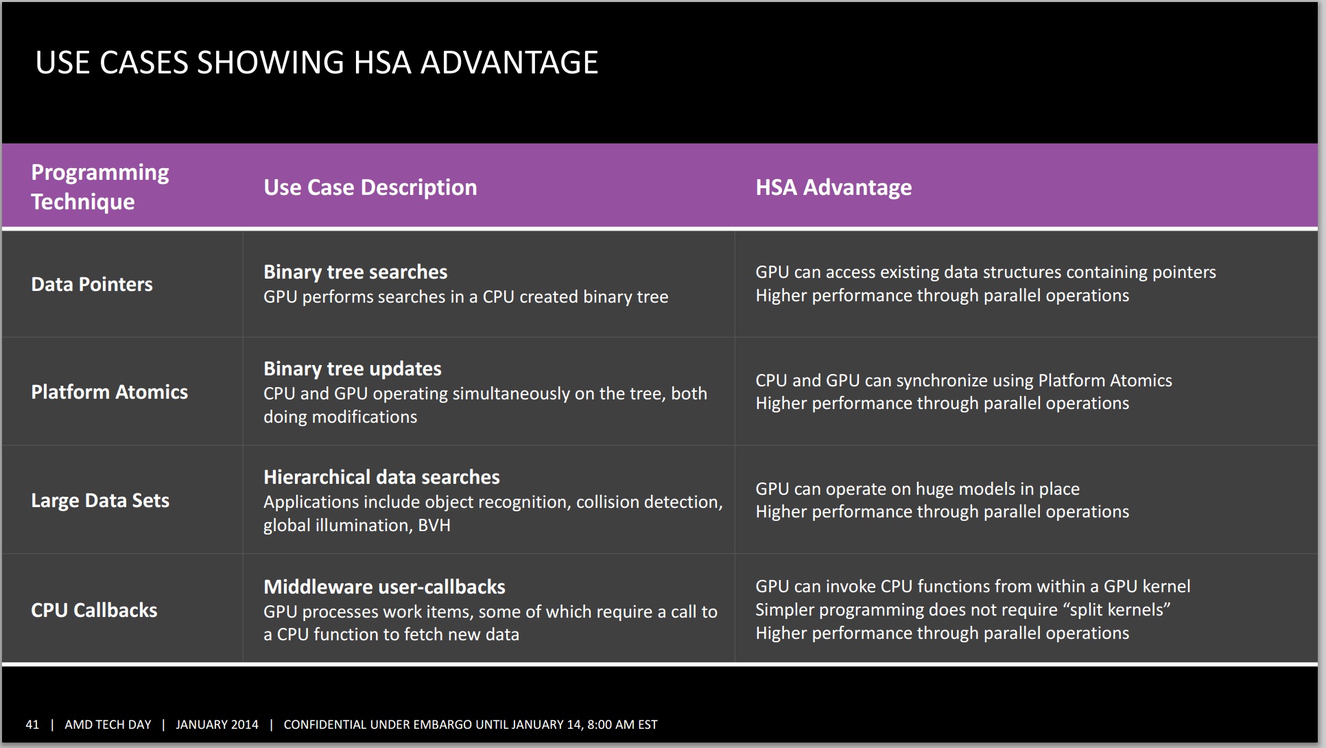
hQ: Optimized Task Queuing in HSA
Heterogeneous Queuing is an odd term for those not in the know. What we have here is a series of code that calls upon another function during its processing, one which requires the performance of another device. Say for example I am running a mathematical solver, and part of the code that runs on the GPU requires CPU assistance in computing. The way the threads are handled is coined ‘heterogeneous queuing’. HSA brings three new capabilities in this context to Kaveri and other HSA systems compared to previous-gen APUs.
User-mode queuing: In most GPGPU APIs, the CPU queues jobs/kernels for the GPU to execute. This queuing goes through the GPU driver and requires some system calls. However, in HSA the queuing can be done in user-mode which will reduce the overhead of job dispatch. The lower-latency of dispatch will make it feasible to efficiently queue even relatively small jobs to the GPU.
Dynamic parallelism: Typically the CPU queues work for the GPU but the GPU could not enqueue work for itself. NVIDIA introduced the capability for GPU kernels to call other GPU kernels with the GK110/Titan and named this dynamic parallelism. HSA systems will include dynamic parallelism.
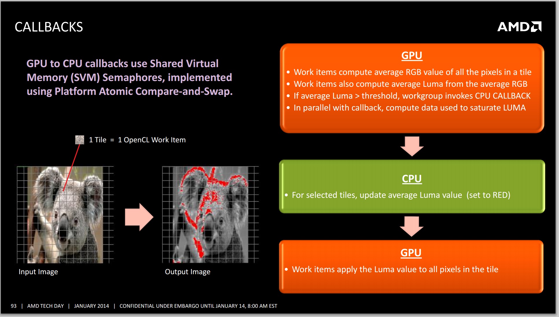
CPU callbacks: With Kaveri, not only will the GPU be able to queue work for itself, it will be able to queue CPU callback functions. This capability goes beyond competitor offerings. CPU callbacks are quite useful in many situations, for example CPU callbacks maybe required to call system APIs that cannot run on the GPU, legacy CPU code that has not yet been ported to the GPU or may simply be code that is more complex, and thus suitable on the CPU.
Programming Tools Roadmap
Given that many users write in different languages for many different purposes, AMD has to have a multifaceted approach when it comes to providing programming tools.
Now we examine part of the software roadmap for programming tools for HSA:
Base HSA stack: Base HSA execution stack supporting HSAIL and HSA runtime for Kaveri is expected to become available in Q2 2014.
LLVM: HSAIL is only one piece of the puzzle. While many compiler writers are perfectly happy to directly generate HSAIL from their compilers, many new compilers today are built on top of toolkits like LLVM. AMD will also open-source an HSAIL code generator for LLVM, which will allow compiler vendors using LLVM to generate HSAIL with very little effort. So we may eventually see compilers for languages such as C++, Python or Julia targeting HSA based systems at some point. Along with the work being done in Clang to support OpenCL, the LLVM to HSAIL generator will also simplify the work of building OpenCL drivers for HSA-based systems. In terms of competition, NVIDIA already provides a PTX backend for LLVM.
OpenCL: At the time of launch, Kaveri will be shipping with OpenCL 1.2 implementation. My understanding is that the launch drivers are not providing HSA execution stack and the OpenCL functionality is built on top of their legacy graphics stack built on top of AMDIL. In Q2 2014, a preview driver providing OpenCL 1.2 with some unified memory extensions from OpenCL 2.0 built on top of HSA infrastructure should be released. A driver with support for OpenCL 2.0 built on top of HSA infrastructure is expected in Q1 2015.
C++ AMP: C++ AMP was pioneered by Microsoft and the Microsoft stack is built on top of DirectCompute. DirectCompute does not really expose unified memory, and even Direct3D 11.2 only takes only preliminary steps towards unified memory. Microsoft's C++ AMP implementation targets DirectCompute and thus won't be able to take full advantage of features offered by HSA enabled systems. However, C++ AMP is an open specification and other compiler vendors can write C++ AMP compilers. HSA Foundation member Multicoreware is working with AMD on providing a C++ AMP compiler that generates HSAIL for HSA enabled platforms, and OpenCL SPIR for other platforms (such as Intel).
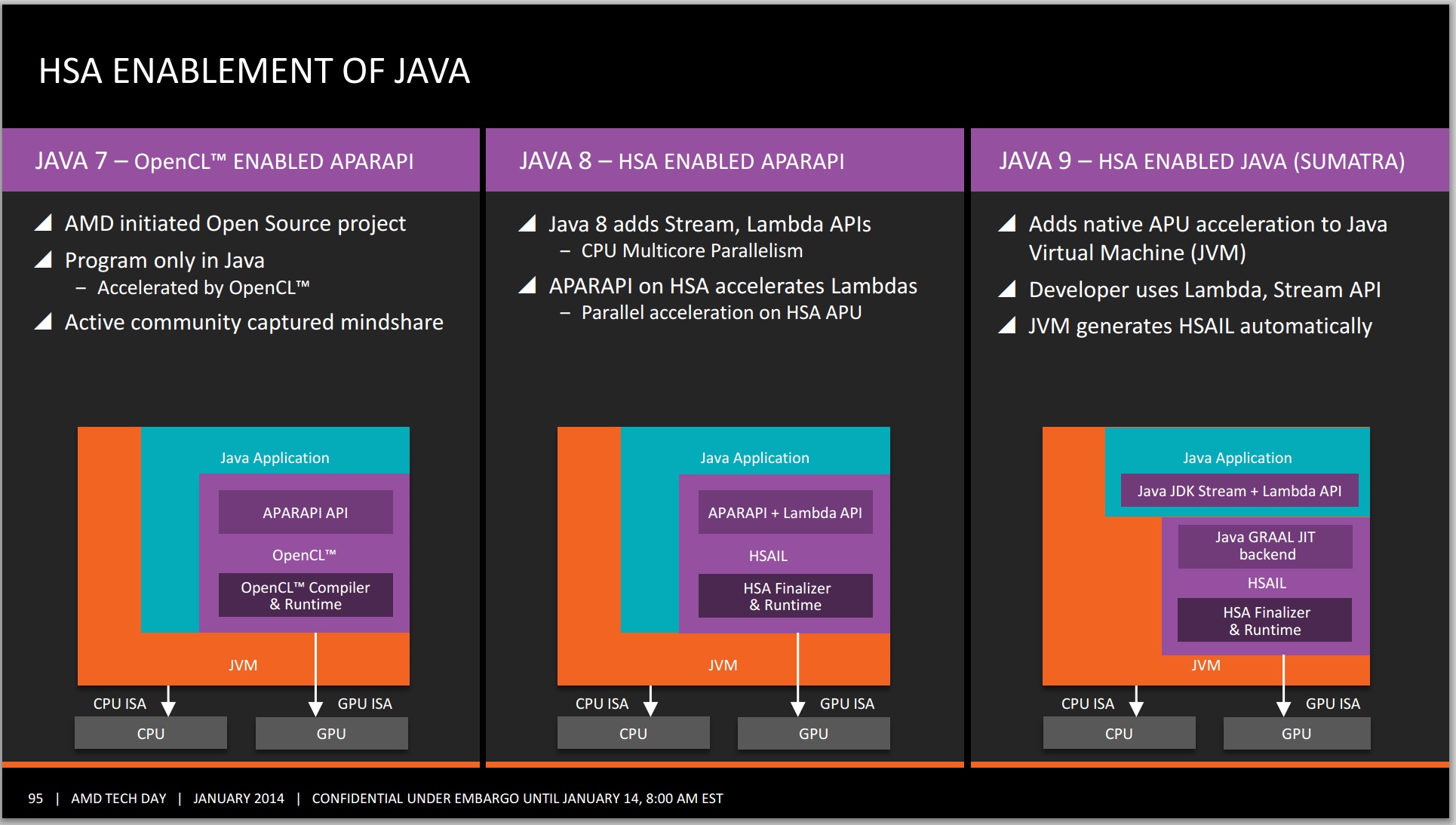
Java "Sumatra" and Aparapi: AMD already provides an API called Aparapi that compiles annotated Java code to OpenCL. AMD will be updating Aparapi to take advantage of HSA in Java 8 and it will be ready sometime in 2014. In addition, Oracle (owner of Java) also announced a plan to target HSA by generating HSAIL from Java bytecode in their HotSpot VM. This is expected to be released with Java 9 sometime in 2015. It will be interesting to watch if IBM, which has announced a partnership with NVIDIA, will also enable HSA backends in its own JVM.
HSA Conclusion
Overall, HSA brings many new capabilities compared to the basic GPGPU compute of AMD platforms to this point. Unified memory in HSA is an extremely exciting step due to the explicit elimination of data-copies, the ability for the GPU to address large amounts of memory and the sharing of complex data structures will enable heterogeneous computing for many more problems. Ability for the GPU to queue kernels for itself, or even do CPU callbacks are both great additions as well. CPU/GPU integration in HSA is definitely a step above the competition and does have the potential of making them more equal peers than the current model. As a compiler writer, I do think that HSA systems will be easier to program for both compiler writers as well as application developers and in the long term does have the potential of making heterogeneous computing more mainstream.
However, HSA will only begin delivering when the software ecosystem takes advantage of HSA capabilities, and this will not happen overnight. While HSA is impressive at the architecture level, AMD also needs to deliver on its software commitments as soon as possible. This not only includes HSA enabled drivers, but also tools such as profilers and debuggers, good documentation and other pieces such as the LLVM backend. I would also like to see more projects for programming languages compiling to HSA, especially open source libraries which AMD are working on for their HSA implementation.
Finally, whether HSA succeeds or fails will also depend upon what direction HSA Foundation members such as Qualcomm, ARM, TI, Imagination tech and Samsung take. At this point, no one other than AMD has announced any HSA-enabled hardware products. Programmers may be reluctant to adopt HSA if it only works on AMD platforms, and there will be slow adoption to make the heterogeneous programming regimen part of the core fundamentals for new programmers. I do expect that the other HSA-enabled products from other vendors will arrive, but the timing will be of importance. In the meantime, competitors such as NVIDIA and Intel are not sitting idle either and we should see better integrated heterogeneous solutions from them soon as well. For now, AMD should be commended for moving the industry forward and for having the most integrated heterogeneous computing solution today.
The GPU
AMD making the move from VLIW4 to the newer GCN architecture makes a lot of sense. Rather than being behind the curve, Kaveri now shares the same GPU architecture as Hawaii based GCN parts; specifically the GCN 1.1 based R9-290X and 260X from discrete GPU lineup. By synchronizing the architecture of their APUs and discrete GPUs, AMD is finally in a position where any performance gains or optimizations made for their discrete GPUs will feed back into their APUs, meaning Kaveri will also get the boost and the bonus. We have already discussed TrueAudio and the UVD/VCE enhancements, and the other major one to come to the front is Mantle.
The difference between the Kaveri implementation of GCN and Hawaii, aside from the association with the CPU in silicon, is the addition of the coherent shared unified memory as Rahul discussed in the previous page.

AMD makes some rather interesting claims when it comes to the gaming market GPU performance – as shown in the slide above, ‘approximately 1/3 of all Steam gamers use slower graphics than the A10-7850K’. Given that this SKU is 512 SPs, it makes me wonder just how many gamers are actually using laptops or netbook/notebook graphics. A quick look at the Steam survey shows the top choices for graphics are mainly integrated solutions from Intel, followed by midrange discrete cards from NVIDIA. There are a fair number of integrated graphics solutions, coming from either CPUs with integrated graphics or laptop gaming, e.g. ‘Mobility Radeon HD4200’. With the Kaveri APU, AMD are clearly trying to jump over all of those, and with the unification of architectures, the updates from here on out will benefit both sides of the equation.
A small bit more about the GPU architecture:
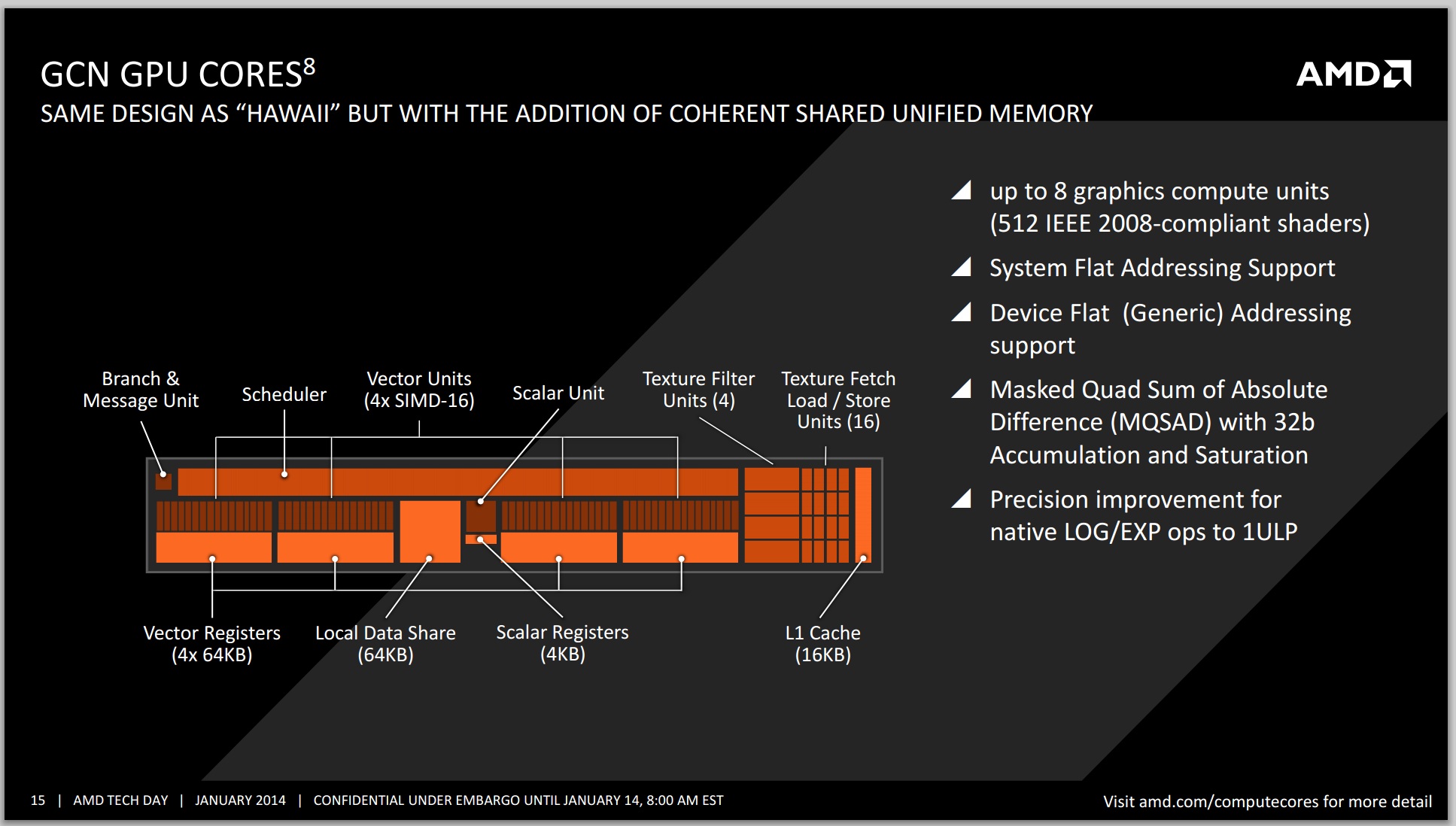
Ryan covered the GCN Hawaii segment of the architecture in his R9 290X review, such as the IEEE2008 compliance, texture fetch units, registers and precision improvements, so I will not dwell on them here. The GCN 1.1 implementations on discrete graphics cards will still rule the roost in terms of sheer absolute compute power – the TDP scaling of APUs will never reach the lofty heights of full blown discrete graphics unless there is a significant shift in the way these APUs are developed, meaning that features such as HSA, hUMA and hQ still have a way to go to be the dominant force. The effect of low copying overhead on the APU should be a big break for graphics computing, especially gaming and texture manipulation that requires CPU callbacks.
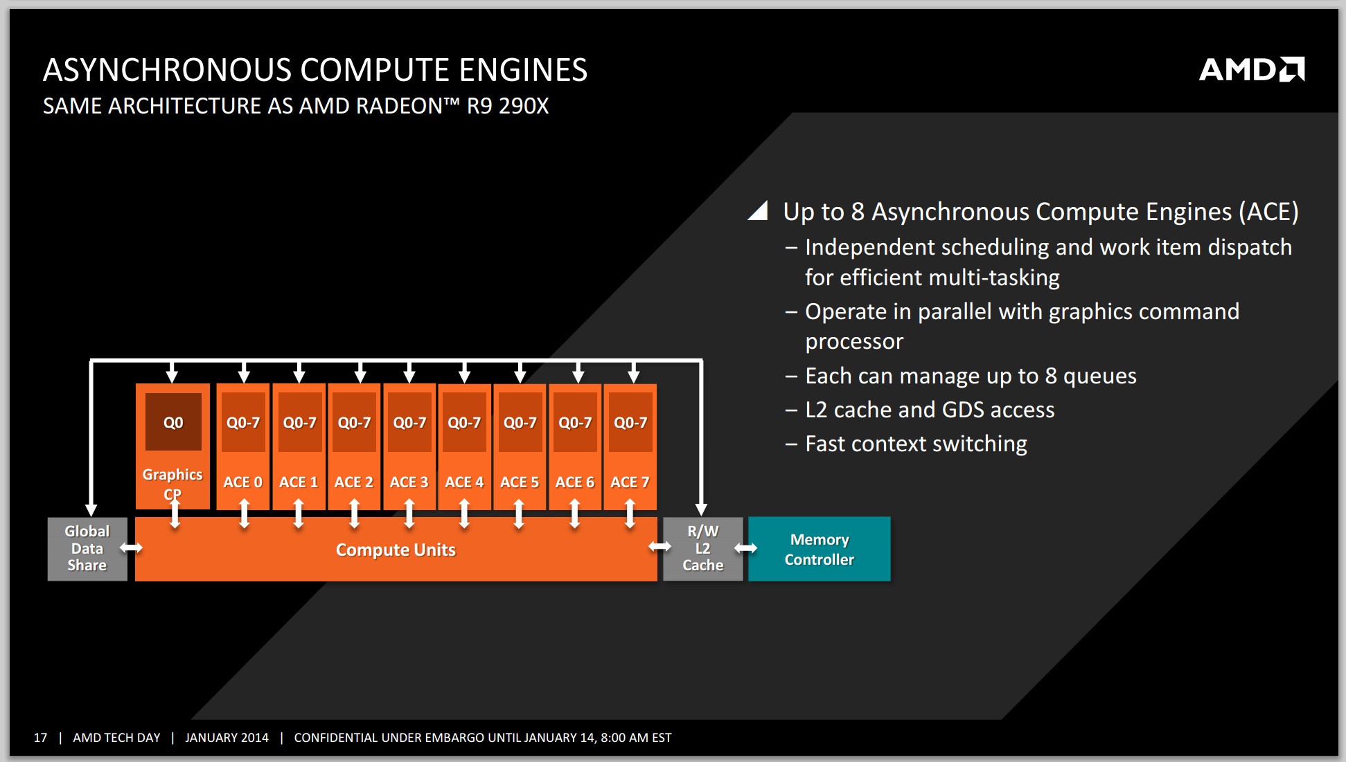
The added benefit for gamers as well is that each of the GCN 1.1 compute units is asynchronous and can implement independent scheduling of different work. Essentially the high end A10-7850K SKU, with its eight compute units, acts as eight mini-GPU blocks for work to be carried out on.
Despite AMD's improvements to their GPU compute frontend, they are still ultimately bound by the limited amount of memory bandwidth offered by dual-channel DDR3. Consequently there is still scope to increase performance by increasing memory bandwidth – I would not be surprised if AMD started looking at some sort of intermediary L3 or eDRAM to increase the capabilities here.

Details on Mantle are Few and Far Between
AMD’s big thing with GCN is meant to be Mantle – AMD's low level API for game engine designers intended to improve GPU performance and reduce the at-times heavy CPU overhead in submitting GPU draw calls. We're effectively talking about scenarios bound by single threaded performance, an area where AMD can definitely use the help. Although I fully expect AMD to eventually address its single threaded performance deficit vs. Intel, Mantle adoption could help Kaveri tremendously. The downside obviously being that Mantle's adoption at this point is limited at best.
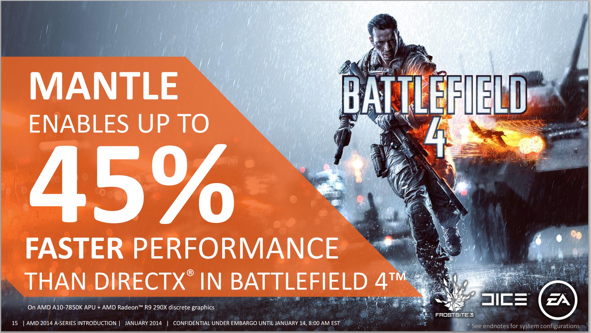
Despite the release of Mantle being held back by the delay in the release of the Mantle patch for Battlefield 4 (Frostbite 3 engine), AMD was happy to claim a 2x boost in an API call limited scenario benchmark and 45% better frame rates with pre-release versions of Battlefield 4. We were told this number may rise by the time it reaches a public release.
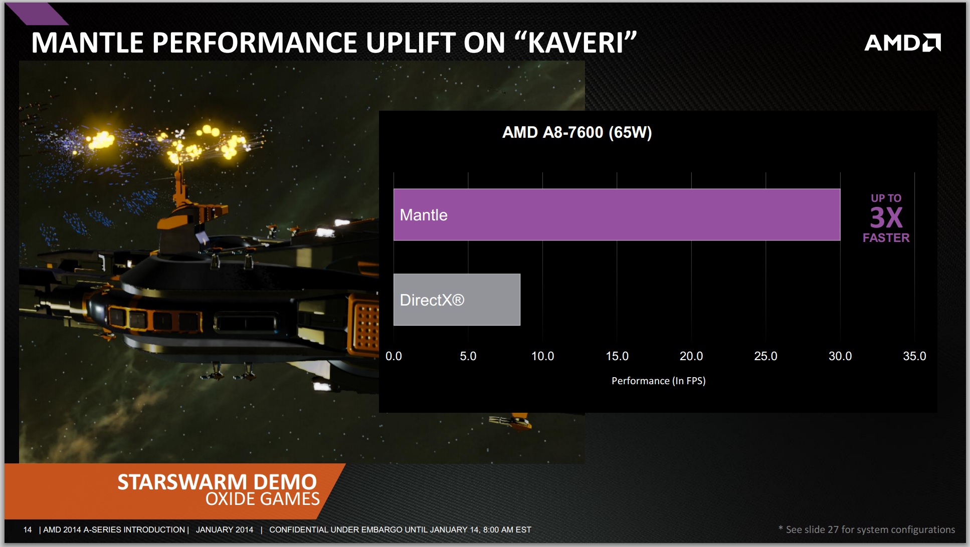

Unfortunately we still don't have any further details on when Mantle will be deployed for end users, or what effect it will have. Since Battlefield 4 is intended to be the launch vehicle for Mantle - being by far the highest profile game of the initial titles that will support it - AMD is essentially in a holding pattern waiting on EA/DICE to hammer out Battlefield 4's issues and then get the Mantle patch out. AMD's best estimate is currently this month, but that's something that clearly can't be set in stone. Hopefully we'll be taking an in-depth look at real-world Mantle performance on Kaveri and other GCN based products in the near future.
Dual Graphics
AMD has been coy regarding Dual Graphics, especially when frame pacing gets plunged into the mix. I am struggling to think if at any point during their media presentations whether dual graphics, the pairing of the APU with a small discrete GPU for better performance, actually made an appearance. During the UK presentations, I specifically asked about this with little response except for ‘AMD is working to provide these solutions’. I pointed out that it would be beneficial if AMD gave an explicit list of paired graphics solutions that would help users when building systems, which is what I would like to see anyway.
AMD did address the concept of Dual Graphics in their press deck. In their limited testing scenario, they paired the A10-7850K (which has R7 graphics) with the R7 240 2GB GDDR3. In fact their suggestion is that any R7 based APU can be paired with any G/DDR3 based R7 GPU. Another disclaimer is that AMD recommends testing dual graphics solutions with their 13.350 driver build, which due out in February. Whereas for today's review we were sent their 13.300 beta 14 and RC2 builds (which at this time have yet to be assigned an official Catalyst version number).
The following image shows the results as presented in AMD’s slide deck. We have not verified these results in any way and are only here as a reference from AMD.

It's worth noting that while AMD's performance with dual graphics thus far has been inconsistent, we do have some hope that it will improve with Kaveri if AMD is serious about continuing to support it. With Trinity/Richland AMD's iGPU was in an odd place, being based on an architecture (VLIW4) that wasn't used in the cards it was paired with (VLIW5). Never mind the fact that both were a generation behind GCN, where the bulk of AMD's focus was. But with Kavari and AMD's discrete GPUs now both based on GCN, and with AMD having significantly improved their frame pacing situation in the last year, dual graphics is in a better place as an entry level solution to improving gaming performance. Though like Crossfire on the high-end, there are inevitably going to be limits to what AMD can do in a multi-GPU setup versus a single, more powerful GPU.
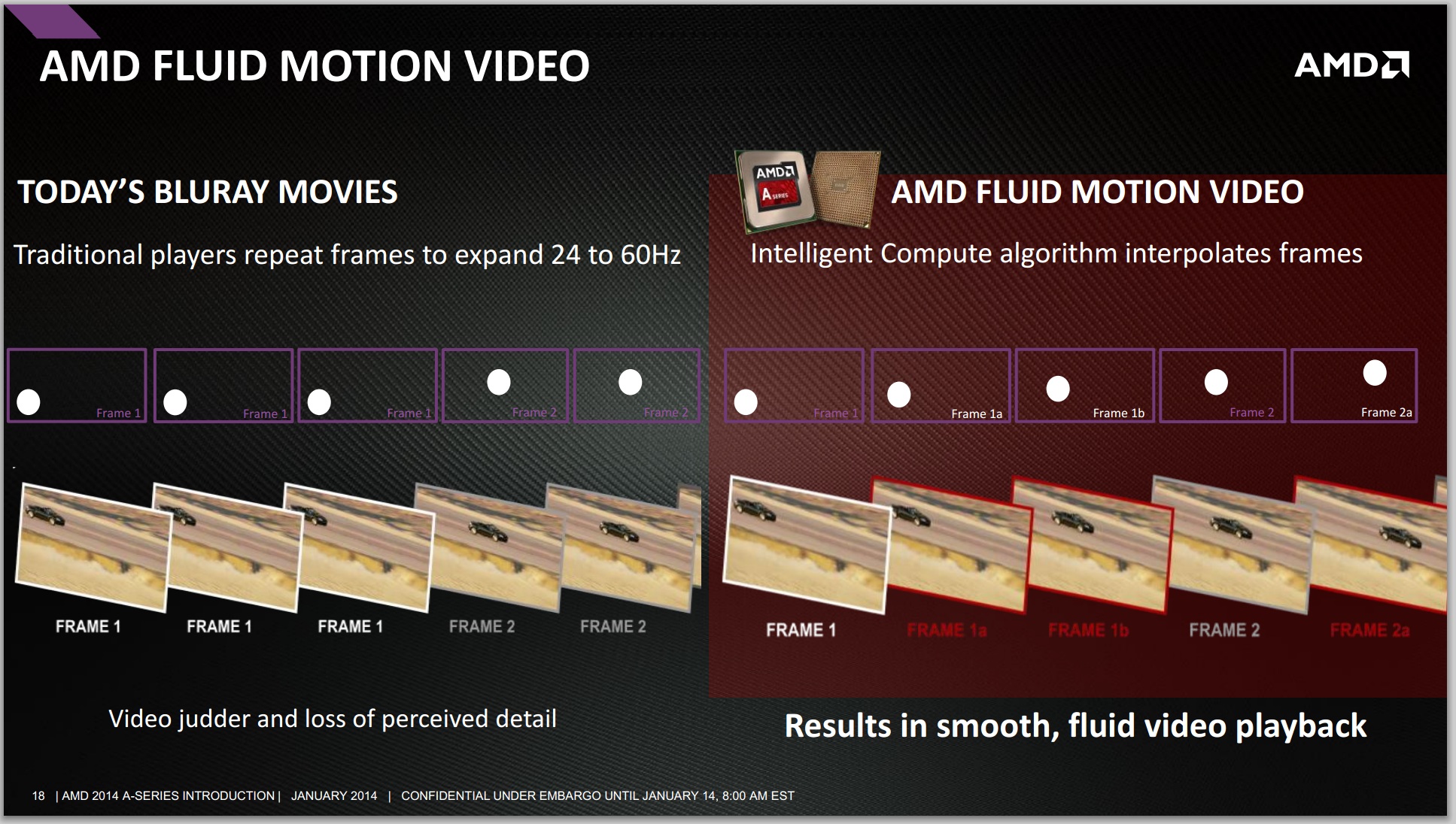
AMD Fluid Motion Video
Another aspect that AMD did not expand on much is their Fluid Motion Video technology on the A10-7850K. This is essentially using frame interpolation (from 24 Hz to 50 Hz / 60 Hz) to ensure a smoother experience when watching video. AMD’s explanation of the feature, especially to present the concept to our reader base, is minimal at best: a single page offering the following:
Socket: FM2+
The new Kaveri processors are built to use the sort-of new FM2+ socket based motherboards. These motherboards fit both FM2+ and FM2 APUs, and thus have been on the market for a good number of months already. However the boards currently on the market may require a BIOS update, and e-tailers shipping motherboards out today may still have the older not-updated revisions in stock, so it is worth confirming that the motherboard you order is updated.
AMD’s generational split on Kaveri is indicative of market pressure and AMD’s history – users like either the processor or the motherboard to be forwards or backwards compatible in terms of compliance. In this case the following table applies:
| Socket Compatibility Chart | ||
| Will Work in FM2 | Will Work in FM2+ | |
| Richland | Yes | Yes |
| Kaveri | No | Yes |
As Kaveri comes with two extra pins that are blocked off with older FM2 motherboards, they are not compatible.
For our testing today, we had sourced the ASRock FM2A88X Extreme6+ and FM2A88X-ITX+ motherboards, both of which will be the focus for review in due course.
Chipset/FCH: A55, A78, A88X
To add some confusion into the mix, AMD is using a mixture of old and new chipsets on FM2+. Kaveri will support the A55, A78 and A88X chipset based motherboards, but not the A75 chipset that was used for Llano/FM1 motherboards. Perhaps more confusing is that while the old Richland APUs will be able to be used on FM2+ with A88X, the older FM2 motherboards will not come with A88X. How about a table to make it clearer:
| Chipset Compatibility Chart | |||
|
Will Work with Llano APUs |
Will Work with Trinity & Richland APUs |
Will Work with Kaveri APUs |
|
| A55 + FM1 | Yes | No | No |
| A55 + FM2 | No | Yes | No |
| A55 + FM2+ | No | Yes | Yes |
| A75 + FM1 | Yes | No | No |
| A75 + FM2 | No | Yes | No |
| A78 + FM2+ | No | Yes | Yes |
| A85X + FM2 | No | Yes | No |
| A88X + FM2+ | No | Yes | Yes |
Though even a table doesn't make the compatibility matrix crystal-clear, it does help to make sense of what users can expect for chipset and sock compatibility. Basically, any A88X motherboard you buy will fit the Kaveri APU. For A78, we are currently under the impression that these will be FM2+ only as well, just do not get confused with older ‘AMD 780L’ Northbridge chipsets that were advertised with A78 in the motherboard name that used the AM3 socket. A55 is almost a free-for-all, with FM1 and FM2 motherboards using it.
As for the differences between the older A85X and A88X chipsets, there are only a few to speak of. Support for PCIe 3.0 is the big one, with any FM2+ and A88X motherboard and Kaveri APU taking full advantage of PCIe 3.0 in all its glory, either as an x16 slot or an x8/x8. A88X still has eight 6 Gbps ports and four USB 3.0 ports native, as well as supporting RAID 0, 1, 5 and 10. The other only upgrade to note is the move to XHCI 1.0.
| Chipset Comparison | |||||
| A55 | A75 | A78 | A85X | A88X | |
| Chipsets |
FM1 FM2 FM2+ |
FM1 FM2 |
FM2+ | FM2 | FM2+ |
| PCIe Generation | 2.0 | 2.0 | 2.0 | 2.0 | 3.0 |
| PCIe Lane Allocation | 1x16 | 1x16 or 2x8 | 1x16 | 1x16 or 2x8 | 1x16 or 2x8 |
| SATA 6/3 Gbps | 0 + 6 | 6 + 0 | 6 + 0 (?) | 8 + 0 | 8 + 0 |
| USB Ports (3/2/1.1) | 0 + 14 + 2 | 4 + 10 + 2 | 4 + 10 + 2 (?) | 4 + 10 + 2 | 4 + 10 + 2 |
| RAID | 0, 1, 10 | 0. 1, 5, 10 | 0. 1, 5, 10 | 0. 1, 5, 10 | 0. 1, 5, 10 |
| TDP | 7.6 W | 7.8 W | 7.8 W ? | 7.8 W | 7.8 W ? |
Unusually for AMD, little information about chipset evolution was provided through the normal channels.
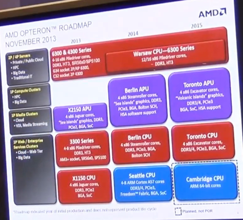
What about FX CPUs, or Server CPUs?
Leaked roadmaps have not been kind to AMD’s FX range. The ‘king’ of the Vishera family of FX CPUs, the quad-module eight-thread FX-9590, looks like it will be the king of the FX line for a little while longer, as shown in this roadmap:
As you might imagine, there is no public comment from AMD about the lack of new FX CPUs with Steamroller cores coming soon.
Depending on which roadmap you look at, AMD’s server offerings are mixed. Some report that During 2014 we will see the launch of “Warsaw” CPUs featuring 12-16 Piledriver cores, and there is no current mention of high-end Steamroller based Opterons at all. The official roadmap from AMD from June shows this, including their ARM server discussion, but a recently leaked roadmap shows that Steamroller will appear in their 1P compute clusters, followed by Excavator in 2015, but Piledriver based 12-16 thread machines will stay at the top of the pile.
Testing Platform
For our Kaveri testing AMD sent us two APUs – the top 95W A10-7850K SKU and the configurable TDP version of the A8-7600 APU, the latter of which can be set at 45W or 65W through the BIOS. The A8-7600 was tested in both power configurations, ultimately the difference between them both being only a few hundred MHz. The 65W configuration is only 200 MHz off the A10-7700K base frequency, and incidentally they both turbo to the same frequency of 3.8GHz.
Kaveri will be the first APU put through the mangle in terms of my new 2014 benchmarking suite, focusing on more compute tasks, video conversion in different software, and more real world scenarios geared for the prosumer.
We must thank the following companies for their contribution to the test beds:
- Many thanks to AMD for supporting us with their APUs, AMD Radeon Memory and test system
- Many thanks to ASRock for supporting us with their FM2A88X Extreme6+ and FM2A88X-ITX+ motherboards and the loan of APUs
- Many thanks to G.Skill for supporting us with their RipjawsX and RipjawsZ memory kits
- Many thanks to OCZ for supporting us with their 1250W Power Supplies and Vertex SSDs
- Many thanks to Samsung for supporting us and AMD with their 840 EVO SSD
- Many thanks to Antec for supporting us and AMD with their 750W High Current Pro PSU
- Many thanks to Xigmatek for supporting us and AMD with their Nebula SFF chassis
Our test setup for AMD is as follows:
| AMD APU TestBed | ||||||||
| SKU | Cores |
CPU / Turbo |
DRAM MHz |
Power | IGP | SPs |
GPU MHz |
|
| Kaveri APUs | A10-7850K | 2M/4T |
3.7 GHz 4.0 GHz |
2133 | 95W | R7 | 512 | 720 MHz |
| A8-7600 | 2M/4T |
3.3 GHz 3.8 GHz |
2133 | 65W | R7 | 384 | 720 MHz | |
| A8-7600 | 2M/4T |
3.1 GHz 3.3 GHz |
2133 | 45W | R7 | 384 | 720 MHz | |
| Richland APUs | A10-6800K | 2M/4T |
4.1 GHz 4.4 GHz |
2133 | 100W | 8670D | 384 | 844 MHz |
| A10-6700T | 2M/4T |
2.5 GHz 3.5 GHz |
1866 | 45W | 8650D | 384 | 720 MHz | |
| A8-6500T | 2M/4T |
2.1 GHz 3.1 GHz |
1866 | 45W | 8550D | 256 | 720 MHz | |
| Trinity APUs | A10-5800K | 2M/4T |
3.8 GHz 4.2 GHz |
2133 | 100W | 7660D | 384 | 800 MHz |
| A8-5500 | 2M/4T |
3.2 GHz 3.7 GHz |
1866 | 65W | 7560D | 256 | 760 MHz | |
| Memory |
AMD Radeon 2 x 8 GB DDR3-2133 10-11-11 1.65V G.Skill RipjawsX 4 x 4 GB DDR3-2133 9-11-11 1.65V G.Skill RipjawsZ 4 x 4 GB DDR3-1866 8-9-9 1.65V |
|||||||
| Motherboards |
ASRock FM2A88X Extreme6+ ASRock FM2A88X-ITX+ |
|||||||
| Power Supply | OCZ 1250W ZX Series | |||||||
| Storage | OCZ 256GB Vertex 3 SSDs | |||||||
| Operating System | Windows 7 64-bit SP1 with Core Parking updates | |||||||
| Video Drivers |
Graphics Driver Build 13.300 RC2 for Radeon R7 Catalyst 13.12 for all others |
|||||||
Unfortunately we were not able to source a 65W Richland part in time, however a midrange 65W Trinity part was on hand. The important thing to note is that within each power bracket, both the CPU frequencies and the supported memory changes depending on the architecture and the binning process AMD uses. The benchmarks in this review are run at the processors' maximum supported frequency, rather than any AMD Memory Profiles which the processor can also support via overclocking. This has implications in conjunction with the IPC or MHz difference.
For this review we also took a few Intel processors of varying TDPs:
| Intel TestBed | ||||||||
| SKU | Cores |
CPU / Turbo |
DRAM MHz |
Power | IGP | SPs |
GPU MHz |
|
| Sandy Bridge | i5-2500K | 4C/4T |
3.3 GHz 3.7 GHz |
1600 | 95W | HD 3000 | 12 | 850 |
| Ivy Bridge | i3-3225 | 2C/4T | 3.3 GHz | 1600 | 55W | HD 4000 | 16 | 550 |
| i7-3770K | 4C/8T |
3.5 GHz 3.9 GHz |
1600 | 77W | HD 4000 | 16 | 550 | |
| Haswell | i3-4330 | 2C/4T | 3.5 GHz | 1600 | 54W | HD 4600 | 20 | |
| i7-4770K | 4C/8T |
3.5 GHz 3.9 GHz |
1600 | 84W | HD 4600 | 20 | ||
|
i7-4770R + Iris Pro |
4C/8T |
3.2 GHz 3.9 GHz |
1600 | 65W | HD 5200 | 40 | ||
| Memory | ADATA XPG 2 x 8 GB DDR3L-1600 9-11-9 1.35V | |||||||
| Motherboards | ASUS Z87 Gryphon | |||||||
| Power Supply | OCZ 1250W ZX Series | |||||||
| Storage | OCZ 256GB Vertex 3 SSDs | |||||||
| Operating System | Windows 7 64-bit SP1 with Core Parking updates | |||||||
| Video Drivers |
15.28.20.64.3347 for HD 3000 15.33.8.64.3345 for HD 4000+4600 |
|||||||
Unfortunately our stock of i5 and i3 processors is actually rather limited – Intel prefers to source the i7s when we review those platforms, but I was able to use a personal i3-3225 from my NAS and we sourced the Haswell i3 as well. Given that Ganesh has the BRIX Pro in for review, I asked him to run as many benchmarks from our gaming suite as I could, to see how well Intel's Haswell eDRAM (Crystalwell) equipped processors stand up to Kaveri’s GCN mêlée.
For reference we also benchmarked the only mid-range GPU to hand - a HD 6750 while connected to the i7-4770K.
Overclocking and Underclocking the A10-7850K
As part of the final testing for this review we did some basic overclocking on the A10-7850K processor. Despite our processor being an engineering sample, we would assume that it is as close/identical to the retail silicon as you can get, given that this is meant to be a review on which people make purchasing decisions.
Our A10-7850K CPU starts out with a peak voltage under load of 1.24 volts when running OCCT. From this point we clocked back to 3.5 GHz and 1.100 volts, with a full-on CPU load line calibration and adjusted turbo mode to equal the base clock. Our standard overclocking test applies – OCCT for five minutes, PovRay, and new for 2014, a run of LuxMark. At our settings, we test the system for stability by running these tests. If the system fails, the CPU voltage is raised 0.025 volts until the system is stable during testing. When stable, the system multiplier is then raised and our testing moves on to the new MHz range.
Our results are as follows:
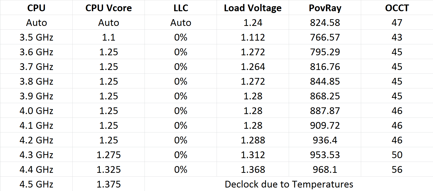
There was an unexpected jump in the voltage required to move from 3.5 GHz to 3.6 GHz (likely hitting the limits of what we can easily attain on this process). The system would not remain stable until 1.225 volts as set in the BIOS.
We also did the power tests, measuring the power draw at the wall as the delta between idle and OCCT load:
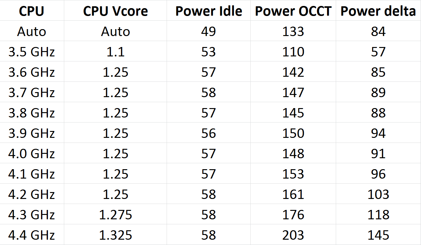
As expected, raising the voltage has a significant effect on the power consumption of the processor. One thing I should point out is that even at stock, the power delivery VRMs were getting very hot to touch – so much in fact that the system generated significant errors without an active fan on them. This got worse as the system was overclocked. I am not sure if this is an effect of the platform or the motherboard, but it will be something to inspect in our motherboard reviews going forward.
CPU Performance
I often make a big song and dance about real world benchmarks being the main focus of a reviewer. Synthetics often stress parts of the CPU and distort advantages that a CPU might have and thus not affect you or me in the same manner when using the machine normally. For 2014 I have updated my usual benchmarking set, to include more video encoding and an image converter that takes 2D images and performs algorithms to convert the data into a 3D model. Some 2013 benchmarks are still here, showing what can be done, and to bring parity to previous CPU reviews, some synthetics are also included.
Agisoft Photoscan v1.0 - link
Our new main benchmark to AnandTech is provided by Agisoft. Their Photoscan software creates 3D models from 2D images, a process which is very computationally expensive. The algorithm is split into four distinct phases, and different phases of the model reconstruction require either fast memory, fast IPC, more cores, or even OpenCL compute devices to hand. Agisoft supplied us with a special version of the software to script the process, where we take 50 images of a stately home and convert it into a medium quality model. This benchmark typically takes around 15-20 minutes on a high end PC on the CPU alone, with GPUs reducing the time.
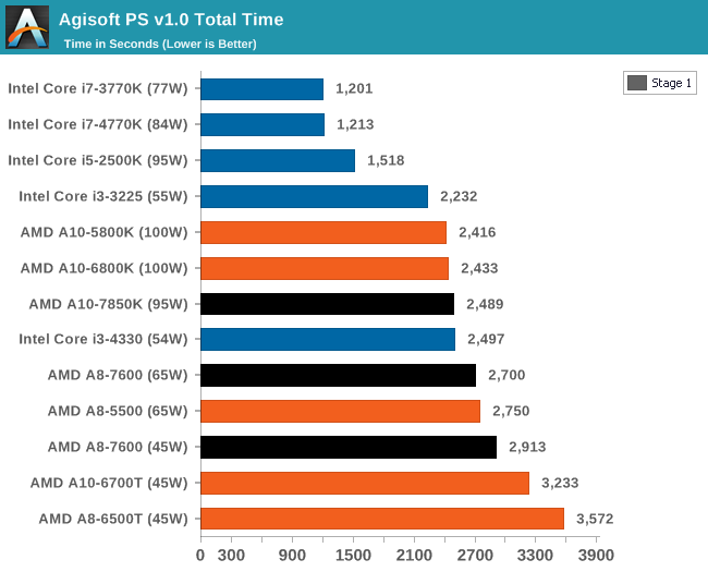
AMD suffers in overall time due to the lack of full-blooded cores and the reliance on single threaded performance in certain parts of the algorithm.
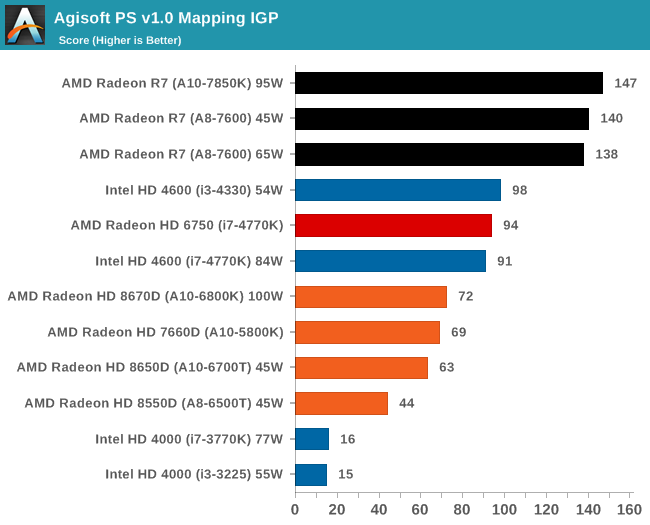
The second stage of the benchmark can be accelerated by the IGP of an APU, and as a result we can see the power of the high end APUs for this work can outshine any CPU we tested today. This is really the promise of HSA, it's just going to take a while to get there for most apps.
3D Particle Movement - link
3DPM is a self-penned benchmark, taking basic 3D movement algorithms used in Brownian Motion simulations and testing them for speed. High floating point performance, MHz and IPC wins in the single thread version, whereas the multithread version has to handle the threads and loves more cores.
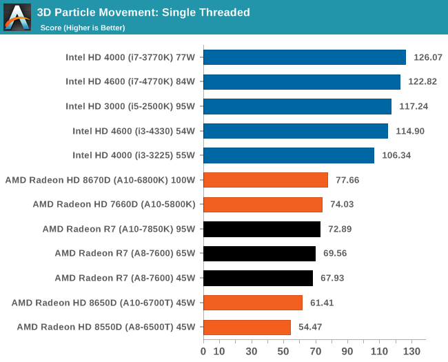
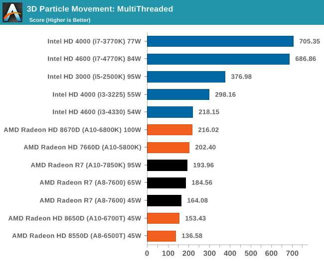
AMD is still suffering a lack of FP performance in our 3DPM benchmark.
WinRAR 5.01 - link
Our WinRAR test from 2013 is updated to the latest version of WinRAR at the start of 2014. We compress a set of 2867 files across 320 folders totaling 1.52 GB in size – 95% of these files are small typical website files, and the rest (90% of the size) are small 30 second 720p videos.
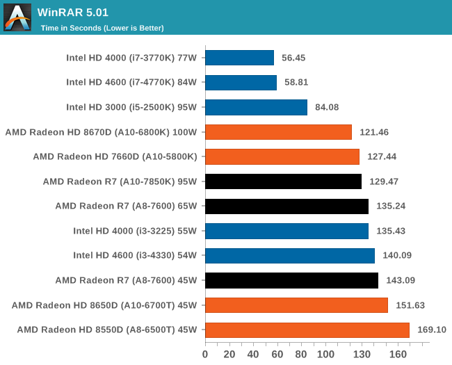
WinRAR loves IPC from the high end Intel chips, but even against the older i5-2500K there is still a deficit. The 45W Kaveri APU however is within fighting distance of its main rival.
FastStone Image Viewer 4.9 - link
Similarly to WinRAR, the FastStone test us updated for 2014 to the latest version. FastStone is the program I use to perform quick or bulk actions on images, such as resizing, adjusting for color and cropping. In our test we take a series of 170 images in various sizes and formats and convert them all into 640x480 .gif files, maintaining the aspect ratio. FastStone does not use multithreading for this test, and thus single threaded performance is often the winner.
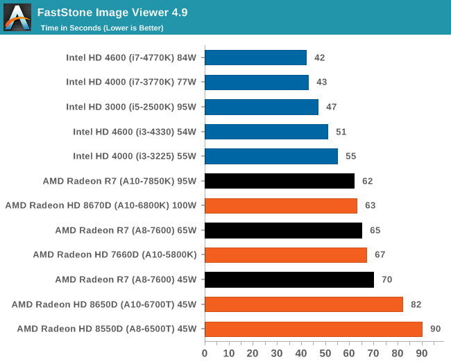
FastStone wants single threaded performance, so Intel wins here again.
CPU Performance: Continued
Xilisoft Video Converter 7 - link
The XVC test I normally do is updated to the full version of the software, and this time a different test as well. Here we take two different videos: a double UHD (3840x4320) clip of 10 minutes and a 640x266 DVD rip of a 2h20 film and convert both to iPod suitable formats. The reasoning here is simple – when frames are small enough to fit into memory, the algorithm has more chance to apply work between threads and process the video quicker. Results shown are in seconds and time taken to encode. XVC also offers acceleration via CUDA and AMD APP, so if these are available on the CPU we offer results with and without.
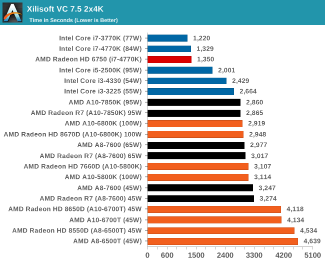
With large frame data, the IGP on Kaveri does not particularly help much.
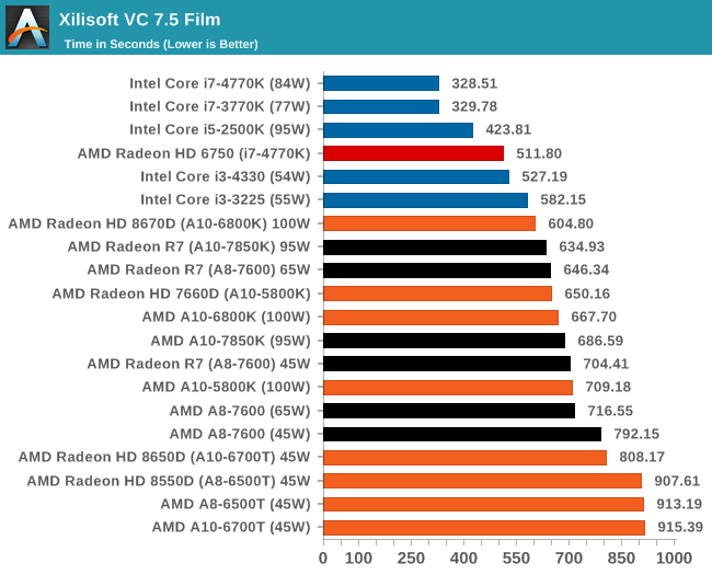
For smaller frames however, there is an advantage to enabling the AMD APP function.
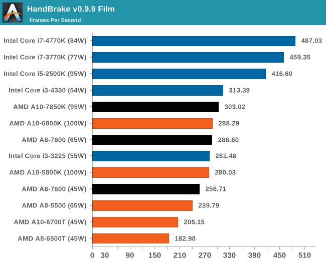
HandBrake v0.9.9 - link
For HandBrake we do the same files as XVC but convert them into the default format Handbrake offers upon loading the software. Results shown are in Frames Per Second.
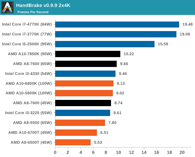
Handbrake loves cores, threads and MHz
Adobe After Effects 6
Published by Adobe, After Effects is a digital motion graphics, visual effects and compositing software package used in the post-production process of filmmaking and television production. For our benchmark we downloaded a common scene in use on the AE forums for benchmarks and placed it under our own circumstances for a repeatable benchmark. We generate 152 frames of the scene and present the time to do so based purely on CPU calculations.
7-Zip 9.2 - link
As an open source compression tool, 7-Zip is a popular tool for making sets of files easier to handle and transfer. The software offers up its own benchmark, to which we report the result.
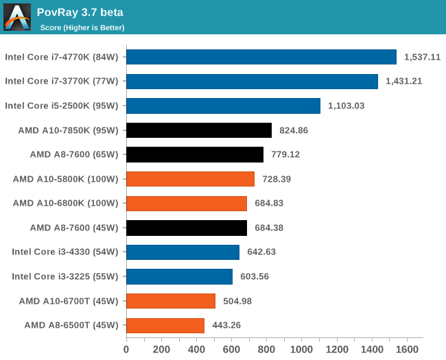
PovRay 3.7 - link
PovRay historically loves threads, MHz and IPC. The standard benchmark from PovRay is what we use to test here.
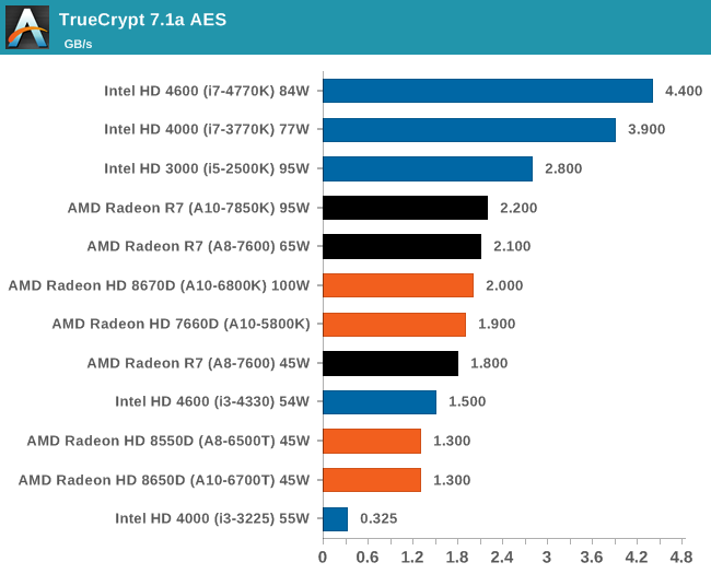
TrueCrypt 7.1a - link
TrueCrypt is an off the shelf open source encoding tool for files and folders. For our test we run the benchmark mode using a 1GB buffer and take the mean result from AES encryption.
Integrated GPU Performance: BioShock Infinite
The first benchmark in our test is Bioshock Infinite, Zero Punctuation’s Game of the Year for 2013. Bioshock Infinite uses the Unreal Engine 3, and is designed to scale with both cores and graphical prowess. We test the benchmark using the Adrenaline benchmark tool and their three default settings of Performance (1280x1024, Low), Quality (1680x1050, Medium/High) and Xtreme (1920x1080, Maximum) noting down the average frame rates and the minimum frame rates.
Bioshock Infinite, Performance Settings
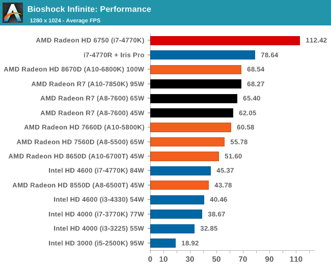
For BI: Performance we see the Iris Pro being top of the IGPs, although the next six in the list are all AMD. The Kaveri cores are all between the 6800K and 5800K for this test, and all comfortably above 60 FPS average.
Bioshock Infinite, Quality Settings
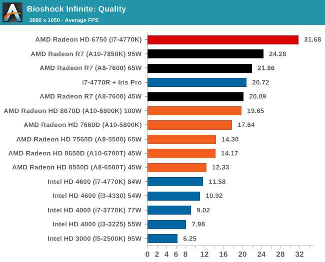
For the quality settings, the Iris Pro starts to struggle and all the R7 based Kaveri APUs jump ahead of the A10-6800K - the top two over the Iris Pro as well.
Bioshock Infinite, Xtreme Settings
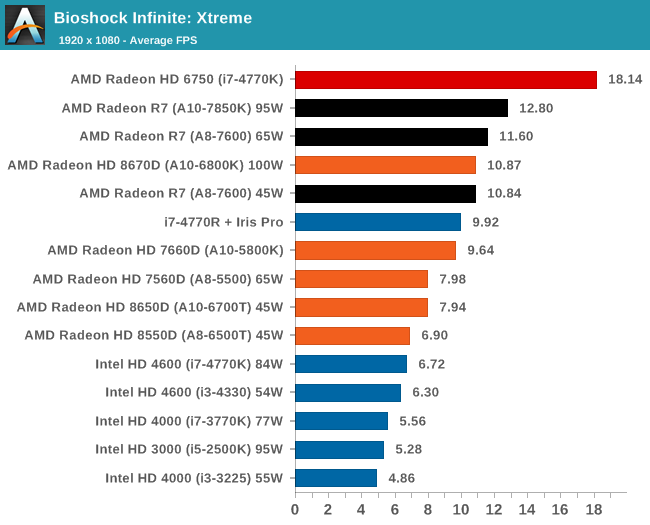
The bigger the resolution, the more the Iris Pro suffers, and Kaveri takes three out of the top four IGP results.
Integrated GPU Performance: Tomb Raider
The second benchmark in our test is Tomb Raider. Tomb Raider is an AMD optimized game, lauded for its use of TressFX creating dynamic hair to increase the immersion in game. Tomb Raider uses a modified version of the Crystal Engine, and enjoys raw horsepower. We test the benchmark using the Adrenaline benchmark tool and their three default settings of Performance (1280x1024, Low), Quality (1680x1050, Medium/High) and Xtreme (1920x1080, Maximum) noting down the average frame rates and the minimum frame rates.
Tomb Raider, Performance Settings
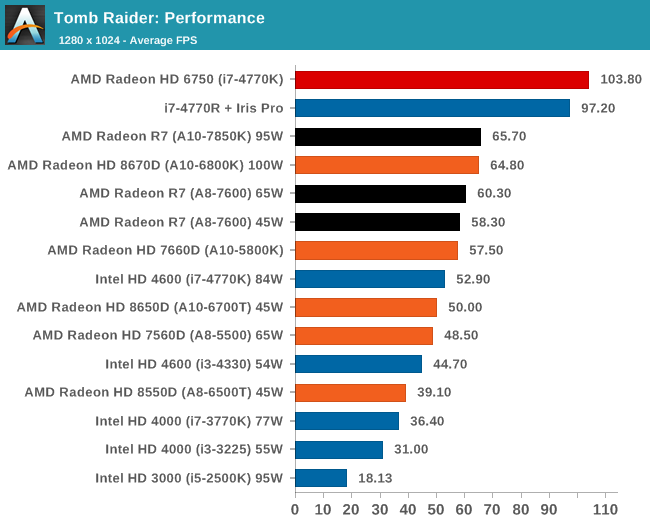
The top IGP for Richland and Kaveri are trading blows in TR.
Tomb Raider, Quality Settings
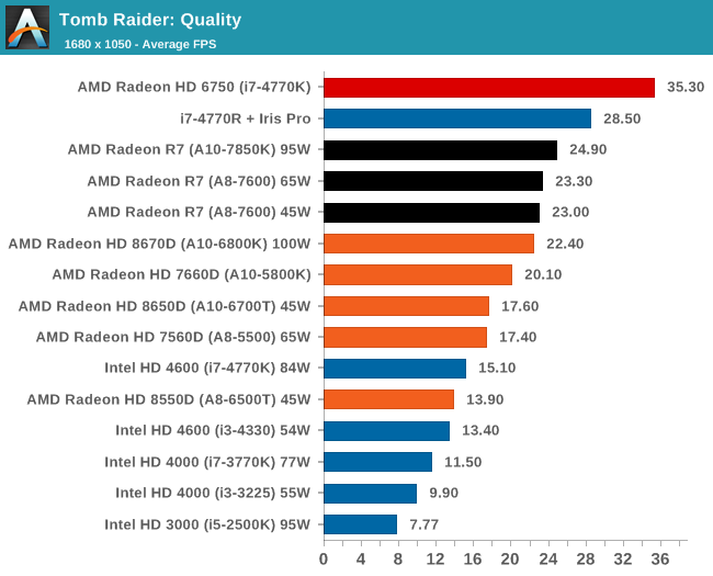
The Iris Pro takes a small lead, while the Kaveri 95W APU show little improvement over Richland. The 45W APU however is pushing ahead.
Tomb Raider, Xtreme Settings
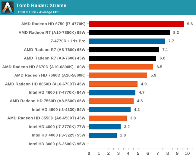
At the maximum resolution, the top Kaveri overtakes Iris Pro, and the 45W Kaveri it still a good margin ahead of the A10-6700T.
Integrated GPU Performance: F1 2013
Next up is F1 2013 by Codemasters. I am a big Formula 1 fan in my spare time, and nothing makes me happier than carving up the field in a Caterham, waving to the Red Bulls as I drive by (because I play on easy and take shortcuts). F1 2013 uses the EGO Engine, and like other Codemasters games ends up being very playable on old hardware quite easily. In order to beef up the benchmark a bit, we devised the following scenario for the benchmark mode: one lap of Spa-Francorchamps in the heavy wet, the benchmark follows Jenson Button in the McLaren who starts on the grid in 22nd place, with the field made up of 11 Williams cars, 5 Marussia and 5 Caterham in that order. This puts emphasis on the CPU to handle the AI in the wet, and allows for a good amount of overtaking during the automated benchmark. We test at three different levels again: 1280x1024 on Low, 1680x1050 on Medium and 1920x1080 on Ultra. Unfortunately due to various circumstances we do not have Iris Pro data for F1 2013.
F1 2013, Performance Settings
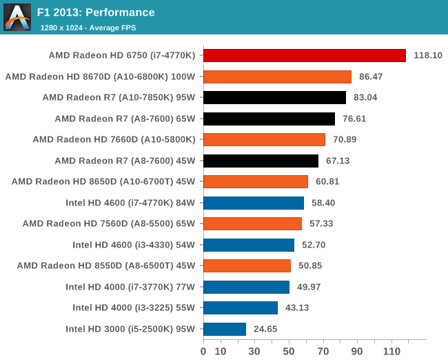
F1 likes AMD here, although moving from Kaveri to Richland at the high end seems a bit of a regression.
F1 2013, Quality Settings
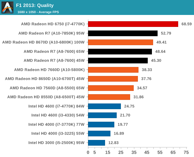
Similarly in the Quality settings, none of the Intel integrated graphics solutions can keep up with AMD, especially Kaveri.
F1 2013, Xtreme Settings
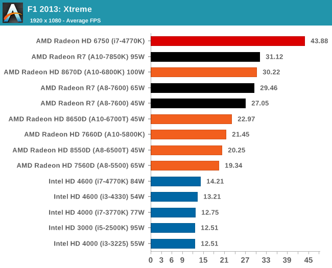
On extreme settings, at 1080p, the top Kaveri APU manages to hit over 30 FPS average during the benchmark. The other A8 Kaveri data is not too far behind.
Integrated GPU Performance: Sleeping Dogs
Sleeping Dogs is a benchmarking wet dream – a highly complex benchmark that can bring the toughest setup and high resolutions down into single figures. Having an extreme SSAO setting can do that, but at the right settings Sleeping Dogs is highly playable and enjoyable. We run the basic benchmark program laid out in the Adrenaline benchmark tool, and their three default settings of Performance (1280x1024, Low), Quality (1680x1050, Medium/High) and Xtreme (1920x1080, Maximum) noting down the average frame rates and the minimum frame rates.
Sleeping Dogs, Performance Settings
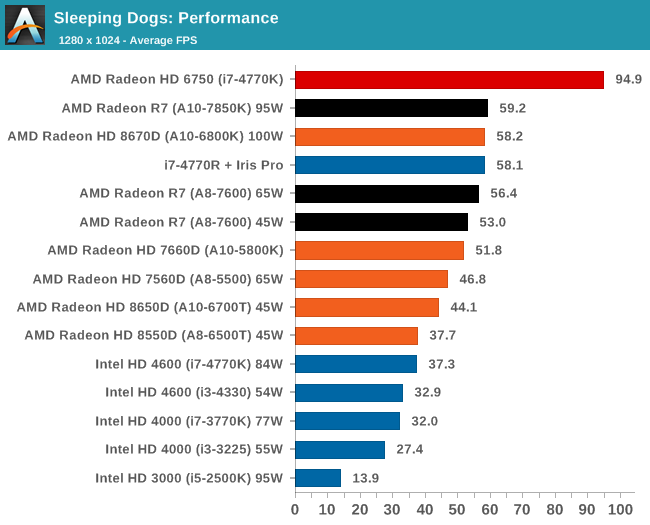
All the AMD APUs tested for this review manage to go above 30 FPS for Sleeping Dogs, with the top end APU nudging at the door of 60 FPS average.
Sleeping Dogs, Quality Settings

The GCN based Kaveri take the top two IGP spots, and Iris Pro is moving down the list by comparison.
Sleeping Dogs, Xtreme Settings
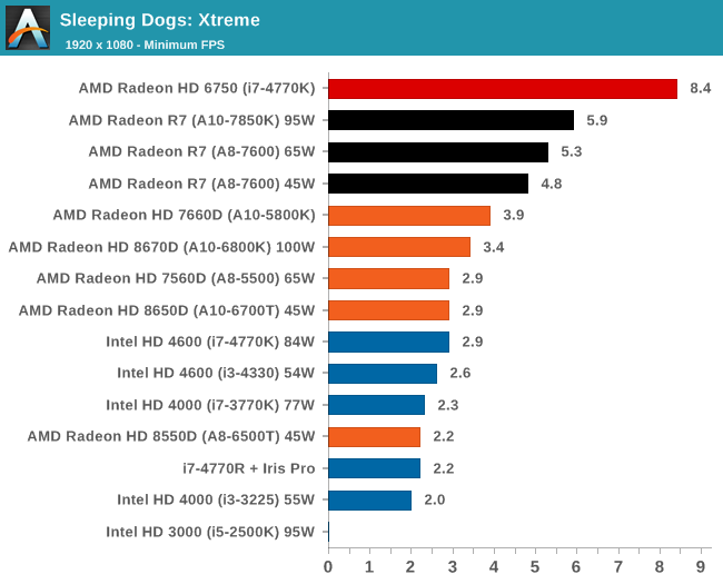
Iris Pro struggles a lot at 1080p in Sleeping Dogs.
Integrated GPU Performance: Company of Heroes 2
The final gaming benchmark is another humdinger. Company of Heroes 2 also can bring the house down, even at very basic benchmark settings. To get an average 30 FPS at any settings using integrated graphics is a challenge, let alone a minimum frame rate of 30 FPS. For this benchmark I use modified versions of Ryan’s batch files more suited for integrated graphics: 1280x1024 on minimum; 1680x1050 on Low and 1920x1080 on Medium.
Company of Heroes 2, Performance Settings
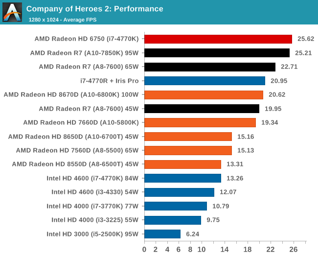
COH2 is demanding enough that even at 1280x1024 and low settings, no platform we tested today can hit 30 FPS average. The 95W Kaveri part does however outshine Richland by almost 25%.
Company of Heroes 2, Quality Settings
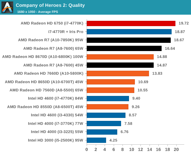
Company of Heroes 2, Xtreme Settings
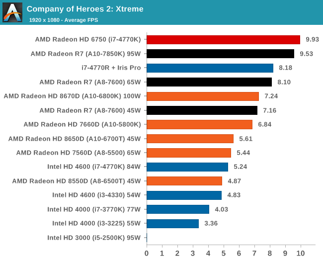
With COH2 extreme settings, the Intel solutions are moving up the minimum FPS ranks to beat AMD.
Processor Graphics: Compute and Synthetics
Our GPU Compute tests are designed to stress the integrated graphics of the system using old and new GPU tools. This is where the benefits of Kaveri should come in – if a benchmark is programmed to take advantage of the GCN architecture then the relevant speed up should be observed. In none of the GCN benefits have any use then we are relying on pure grunt to get the top scores.
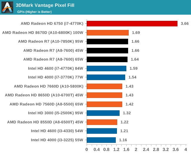
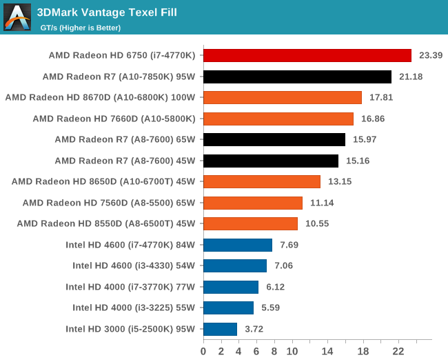
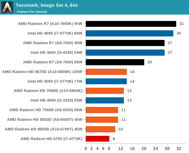
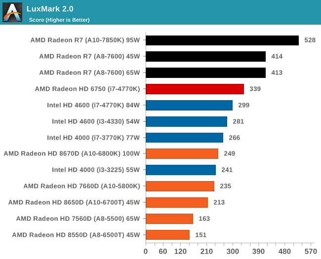
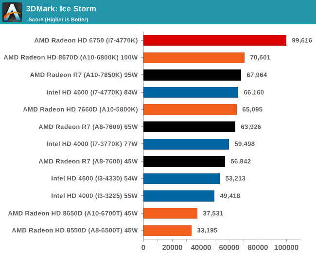
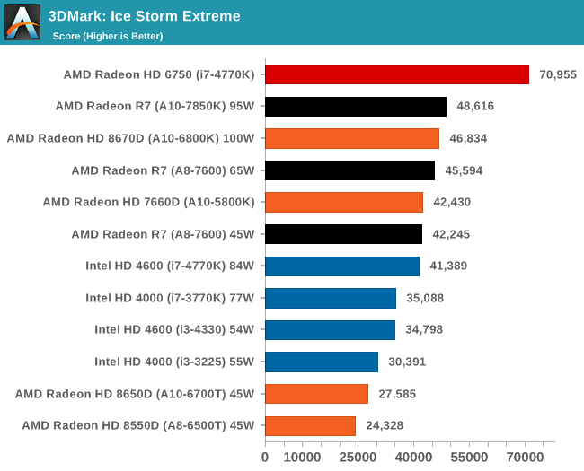
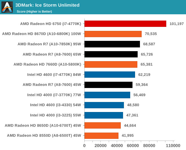
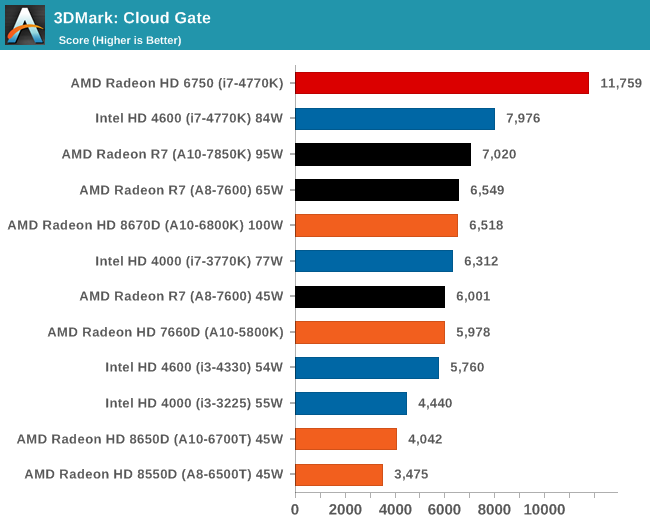
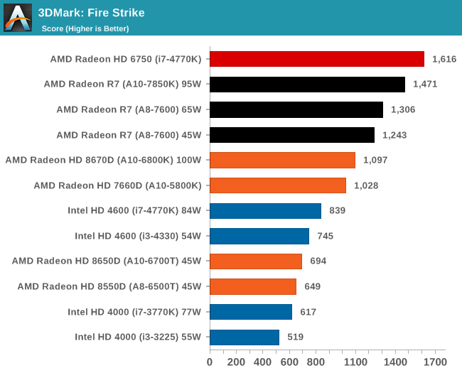
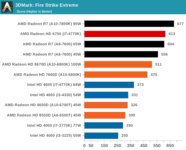
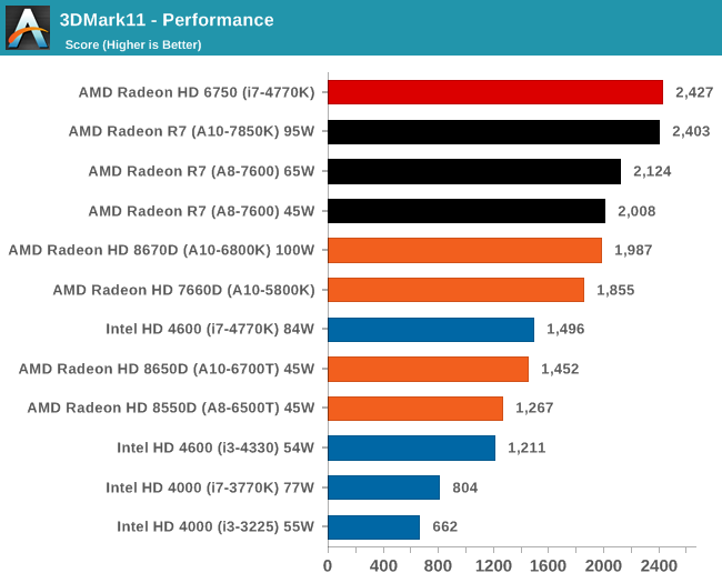
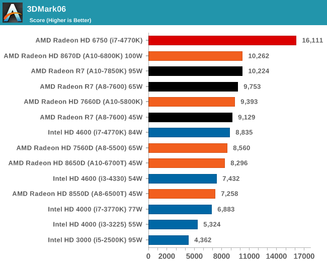
CompuBench CL Fluid GPU + Computer Vision GPU
CompuBench CL is an OpenCL compute benchmark designed to test some common in-use algorithms. Due to the way it is designed, any OpenCL compatible device can run the benchmarks, and as such we have run both the Fluid Dynamics and Computer Vision portions on the CPU and integrated graphics on each processor we have tested. Here are the GPU results.
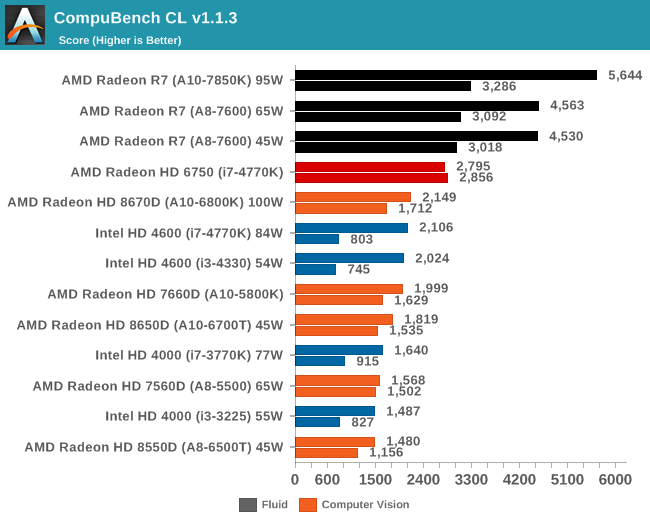
GCN really wins out here, showcasing how important OpenCL compliance can be to extract potential compute.
Drawing Performance Conclusions
As I progressed through the testing for this review, I became aware of trends in two things: absolute performance, in terms of numbers, and generational improvements across platforms. With AMD moving the Bulldozer based architectures from Piledriver in Trinity and Richland to Steamroller in Kaveri, the base CPU design has had a relatively long run in order to be optimized to the limitations on the CPU side. Obviously AMD has also had a chance to change the lithography node in there as well, and as such has optimized for design rather than performance. This matters a great deal when we look at the power banding (45W, 65W, 95W) and performance in each segment.
In order to display just how much Kaveri has grown in relation to the previous generations, I processed our mountain of data to show graphs where percentage gain against the older generations really does matter. As mentioned previously in this review, it all depends on whether the software can take advantage of the new features afforded by the architecture. In this review we have spent a lot of time discussing advantages for Kaveri in terms of compute (HSA, hUMA, hQ) and gaming (Mantle, TrueAudio), but some of these are still a little way off for software integration. So what does that translate to if you are looking for an APU today – does Kaveri still expand its wings with the integration of the GCN architecture, or does it lag behind due to the lithography node no longer being optimized for frequency. The proof is in the results.
IGP Gaming, 1280x1024
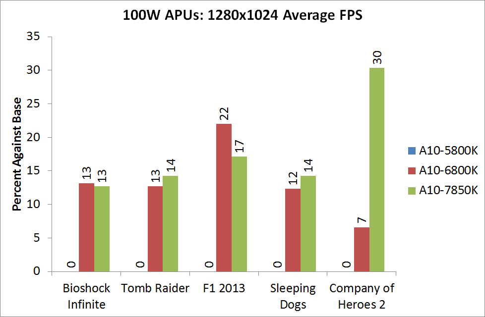
For the 100W APUs at 1280x1024, there is almost no movement between the Richland and the Kaveri APUs, except for Company of Heroes which would seem to leverage the extra SPs more than the MHz available.
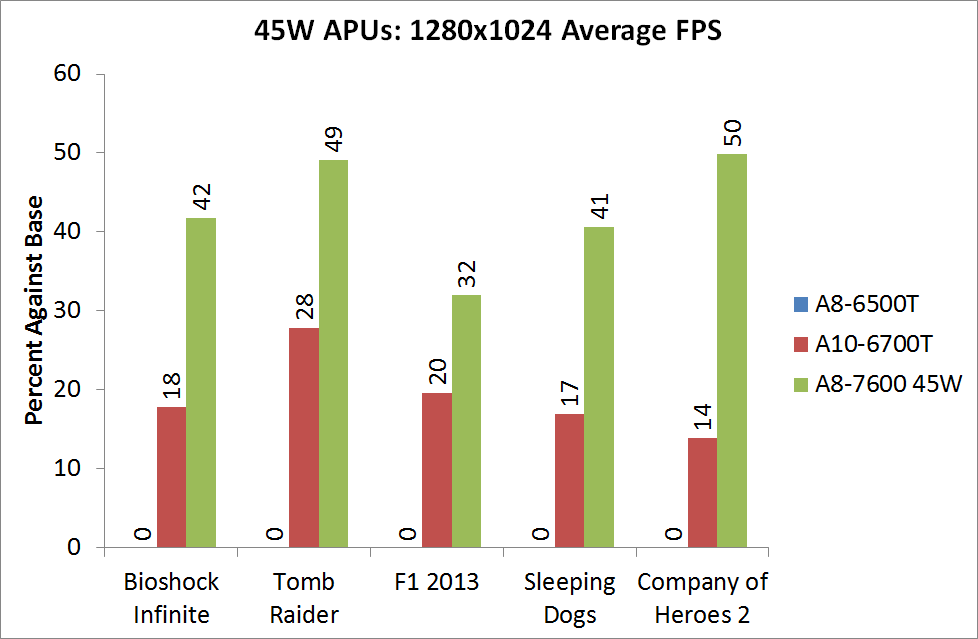
45W APUs are clearly in vogue at 1280x1024, each of them providing a good bump over Richland.
IGP Gaming, 1680x1050
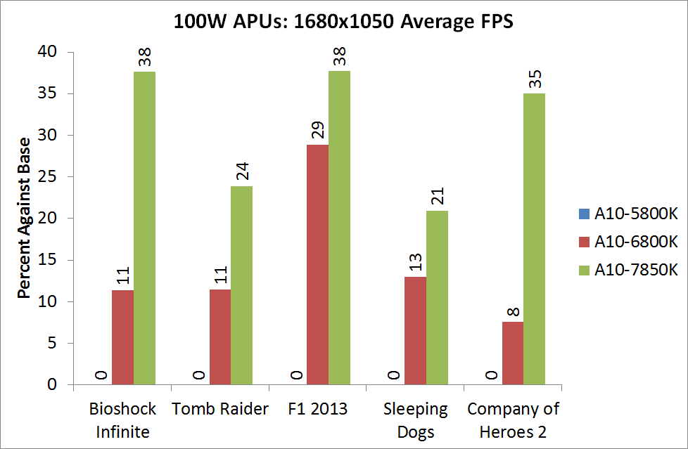
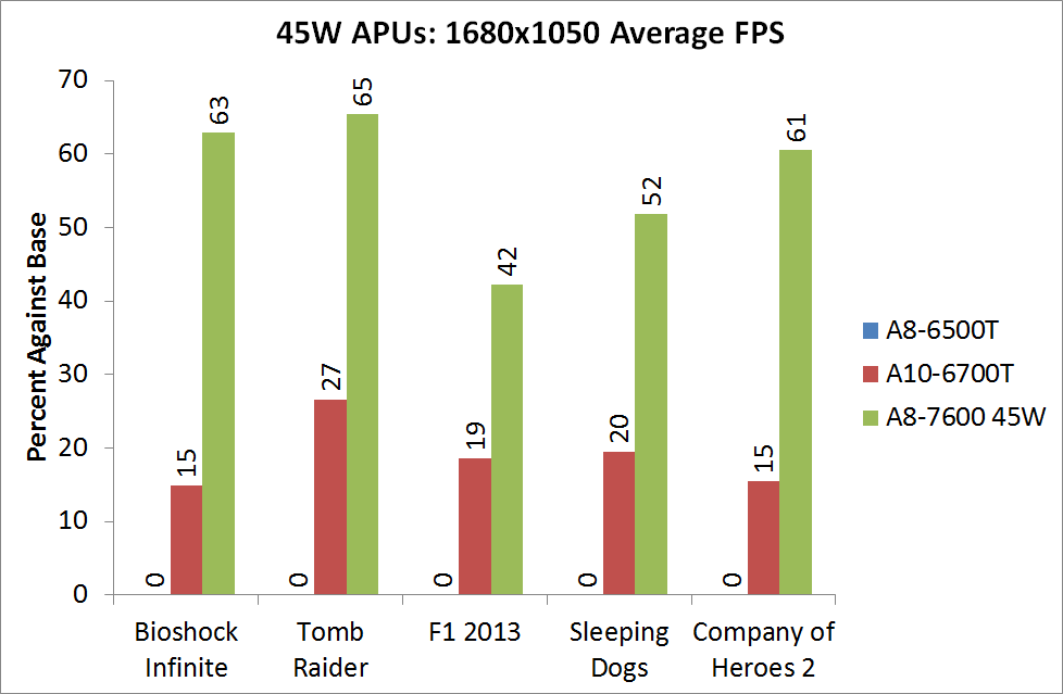
1680x1050 sees more benefit for the 100W APUs, but the 45W APUs still show big leaps.
IGP Gaming, 1920x1080
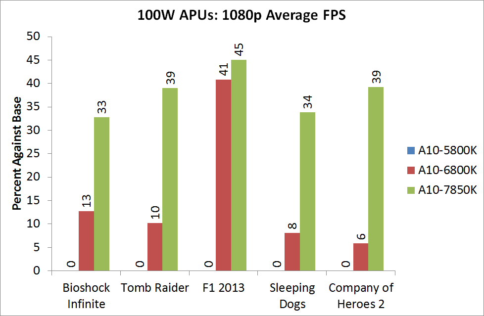

At 1080p the effects are more pronounced all around.
CPU Timed Benchmarks
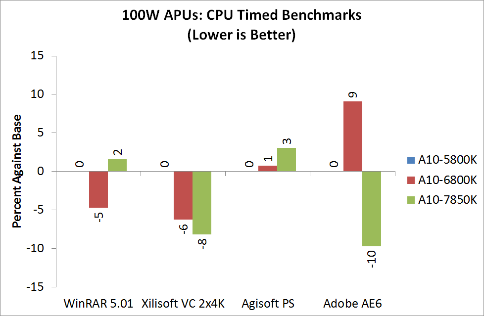
Unfortunately the CPU timed benchmarks at 100W are bit over the place. Here we are dealing with an IPC gain but MHz deficit, and each benchmark has a different way of dealing with it. For Agisoft, MHz wins, but for Xilisoft, the Kaveri improvements work out well for the system.
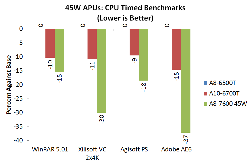
At 45W the situation is a lot more clearer, and the newer APUs have the advantage, especially in Adobe After Effects.
CPU Score Benchmarks
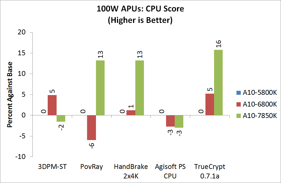

45W still makes the biggest jump when it comes to score based CPU benchmarks.
IGP Synthetics
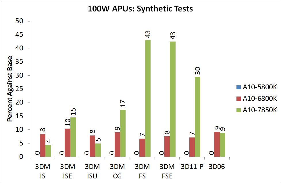
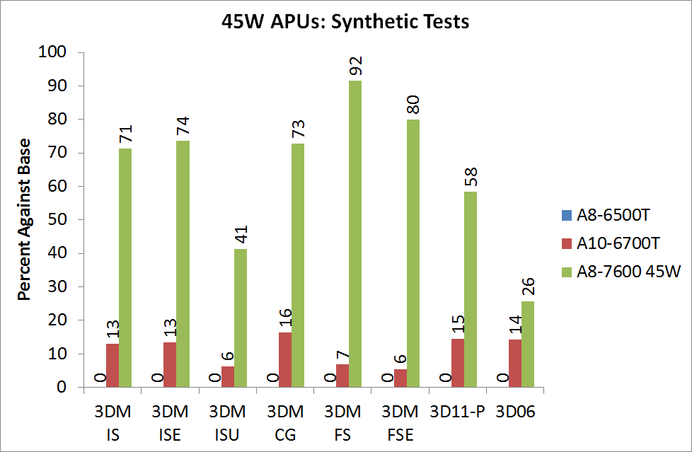
I never like putting much thought into the synthetic results – here both the 100W and the 45W range are showing good improvements all around. 3DMark 06 has the most trouble getting improvements as it relies more on the grunt, rather than the features that Kaveri affords.
IGP Compute
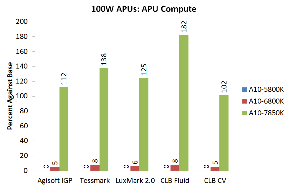
Off the bat we can see just how much of a difference the Kaveri GPU Compute can make over previous APUs. This is still without hUMA fully being in effect while we wait for a proper driver and software stack to become available.
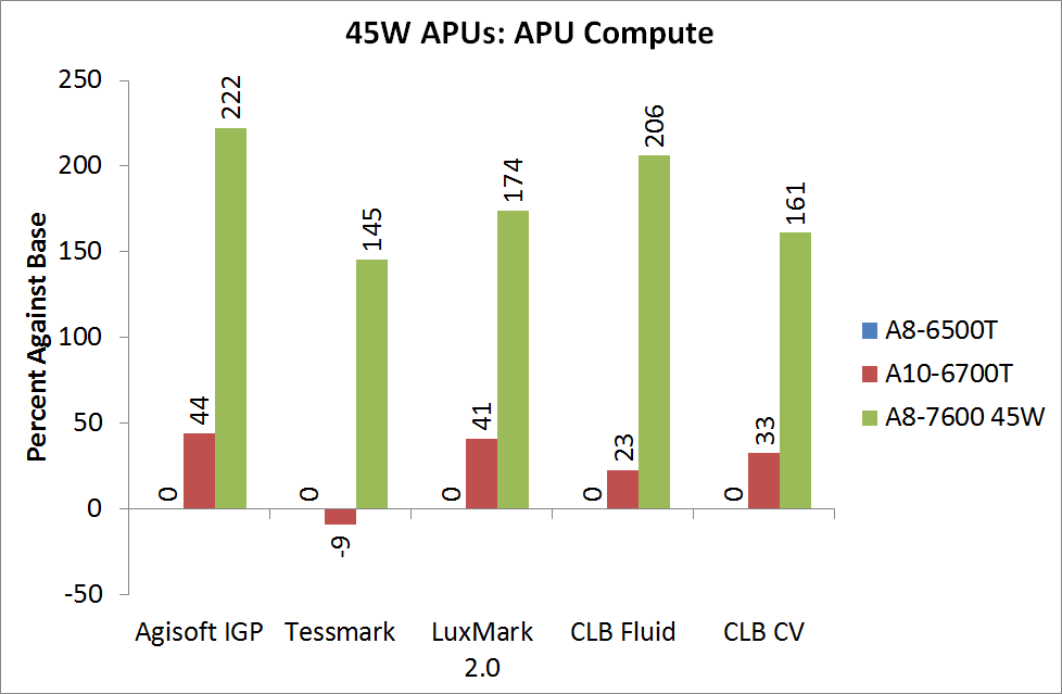
Up to a +222% boost from Kaveri is amazing for a 45W part.
AMD vs Intel
For a little tete-a-tete, putting the 65W Iris Pro up against the 65W Kaveri seems like a good idea. To add to the mix, due to the extreme price difference of Iris Pro in this equation, we also add the 95 W Kaveri for comparison.
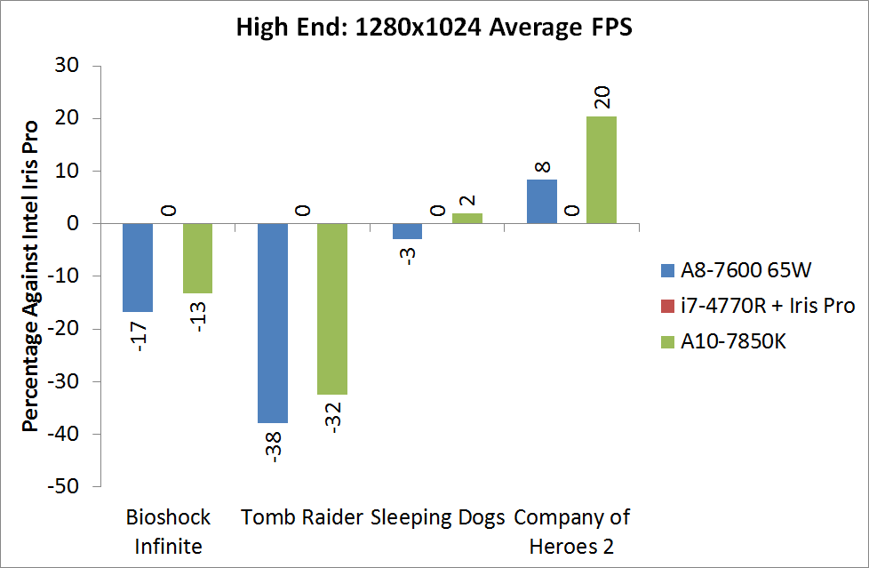
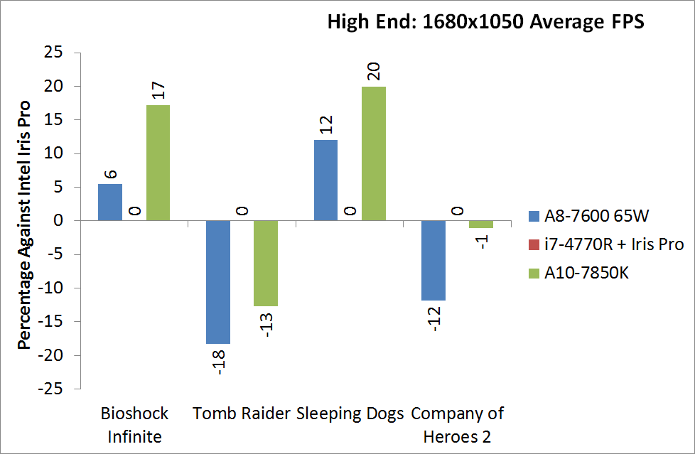
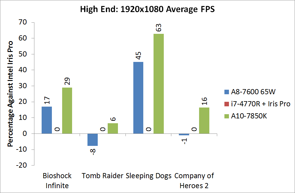
It is interesting to note that at the lower resolutions the Iris Pro wins on most benchmarks, but when the resolution and complexity is turned up, especially in Sleeping Dogs, the Kaveri APUs are in the lead.
Final Words
As with all previous AMD APU launches, we're going to have to break this one down into three parts: CPU, the promise of HSA and GPU.
In a vacuum where all that's available are other AMD parts, Kaveri and its Steamroller cores actually look pretty good. At identical frequencies there's a healthy increase in IPC, and AMD has worked very hard to move its Bulldozer family down to a substantially lower TDP. While Trinity/Richland were happy shipping at 100W, Kaveri is clearly optimized for a much more modern TDP. Performance gains at lower TDPs (45/65W) are significant. In nearly all of our GPU tests, a 45W Kaveri ends up delivering very similar gaming performance to a 100W Richland. The mainstream desktop market has clearly moved to smaller form factors and it's very important that AMD move there as well. Kaveri does just that.
In the broader sense however, Kaveri doesn't really change the CPU story for AMD. Steamroller comes with a good increase in IPC, but without a corresponding increase in frequency AMD fails to move the single threaded CPU performance needle. To make matters worse, Intel's dual-core Haswell parts are priced very aggressively and actually match Kaveri's CPU clocks. With a substantial advantage in IPC and shipping at similar frequencies, a dual-core Core i3 Haswell will deliver much better CPU performance than even the fastest Kaveri at a lower price.
The reality is quite clear by now: AMD isn't going to solve its CPU performance issues with anything from the Bulldozer family. What we need is a replacement architecture, one that I suspect we'll get after Excavator concludes the line in 2015.
In the past AMD has argued that for the majority of users, the CPU performance it delivers today is good enough. While true, it's a dangerous argument to make (one that eventually ends up with you recommending an iPad or Nexus 7). I have to applaud AMD's PR this time around as no one tried to make the argument that CPU performance was somehow irrelevant. Although we tend to keep PR critique off of AnandTech, the fact of the matter is that for every previous APU launch AMD tried its best to convince the press that the problem wasn't with its CPU performance but rather with how we benchmark. With Kaveri, the arguments more or less stopped. AMD has accepted its CPU performance is what it is and seems content to ride this one out. It's a tough position to be in, but it's really the only course of action until Bulldozer goes away.
It's a shame that the CPU story is what it is, because Kaveri finally delivers on the promise of the ATI acquisition from 2006. AMD has finally put forth a truly integrated APU/SoC, treating both CPU and GPU as first class citizens and allowing developers to harness both processors, cooperatively, to work on solving difficult problems and enabling new experiences. In tests where both the CPU and GPU are used, Kaveri looks great as this is exactly the promise of HSA. The clock starts now. It'll still be a matter of years before we see widespread adoption of heterogeneous programming and software, but we finally have the necessary hardware and priced at below $200.
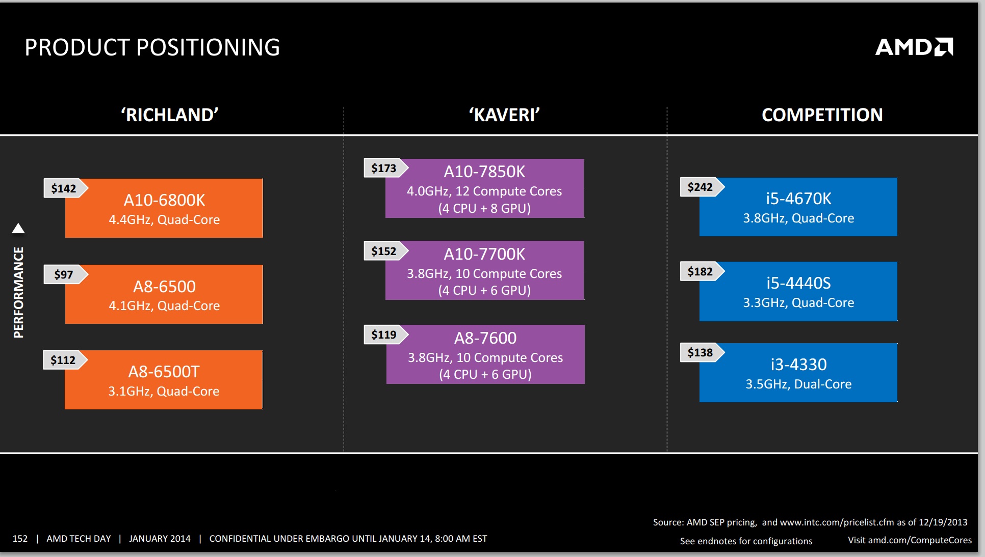
Until then, outside of specific applications and GPU compute workloads, the killer app for Kaveri remains gaming. Here the story really isn't very different than it was with Trinity and Richland. With Haswell Intel went soft on (socketed) desktop graphics, and Kaveri continues to prey on that weakness. If you are building an entry level desktop PC where gaming is a focus, there really isn't a better option. I do wonder how AMD will address memory bandwidth requirements going forward. A dual-channel DDR3 memory interface works surprisingly well for Kaveri. We still see 10 - 30% GPU performance increases over Richland despite not having any increase in memory bandwidth. It's clear that AMD will have to look at something more exotic going forward though.
For casual gaming, AMD is hitting the nail square on the head in its quest for 1080p gaming at 30 frames per second, albeit generally at lower quality settings. There are still a few titles that are starting to stretch the legs of a decent APU (Company of Heroes is practically brutal), but it all comes down to perspective. Let me introduce you to my Granddad. He’s an ex-aerospace engineer, and likes fiddling with stuff. He got onboard the ‘build-your-own’ PC train in about 2002 and stopped there – show him a processor more than a Pentium 4 and he’ll shrug it off as something new-fangled. My grandfather has one amazing geeky quality that shines through though – he has played and completed every Tomb Raider game on the PC he can get his hands on.
It all came to a head this holiday season when he was playing the latest Tomb Raider game. He was running the game on a Pentium D with an NVIDIA 7200GT graphics card. His reactions are not the sharpest, and he did not seem to mind running at sub-5 FPS at a 640x480 resolution. I can imagine many of our readers recoiling at the thought of playing a modern game at 480p with 5 FPS. In the true spirit of the season, I sent him a HD 6750, an identical model to the one in the review today. Despite some issues he had finding drivers (his Google-fu needs a refresher), he loves his new card and can now play reasonably well at 1280x1024 on his old monitor.
The point I am making with this heart-warming/wrenching family story is that the Kaveri APU is probably the ideal fit for what he needs. Strap him up with an A8-7600 and away he goes. It will be faster than anything he has used before, it will play his games as well as that new HD 6750, and when my grandmother wants to surf the web or edit some older images, she will not have to wait around for them to happen. It should all come in with a budget they would like as well.


