Original Link: https://www.anandtech.com/show/2937
The RV870 Story: AMD Showing up to the Fight
by Anand Lal Shimpi on February 14, 2010 12:00 AM EST- Posted in
- GPUs
The Call
My love/hate relationship with AMD PR continued last year. But lately, it’s been far less hate. Let’s rewind back to the Summer of 2009. I’d been waiting for AMD to call for weeks.
We all knew that the RV870 was going to launch sometime before the end of the year, and we’re normally briefed on new GPUs around a month or so before we get hardware. The rumors said that the launch had been pushed back, but just like clockwork I got a call in June or July of last year. It was my old friend, Chris Hook of AMD PR.
This time he wanted me to come to a press event on a carrier off the coast of California. Sigh.
It’s not that I have anything against carriers. It’s just that all I cared about at that time was the long awaited successor to the RV770. The RV770 was the GPU that unequivocally restored my faith in ATI graphics, an impact shared by others last June. But that’s not how the game is played I’m afraid. AMD promises its management and its partners that they can fill a room (or carrier) up with important press. We get promised access to engineers, useful information and free drinks.
The USS Hornet. GPUs are in there.
I’m not easily swayed by free drinks, but Chris Hook knows me well enough by now to know what I’d appreciate even more.
The Dinner - September 2009
I had to leave dinner earlier than I wanted to. ASUS’ Chairman Jonney Shih was in town and only had one opportunity to meet me before I left Oakland. Whenever either of us happens to be in the same town, we always make our best effort to meet - and I wasn’t going to let him down. In the same vein that Steve Jobs is successful because he is a product guy at heart, running a company best known for its products. Jonney Shih is an engineer at heart, and he runs a company who has always been known for their excellence in engineering. This wasn’t just another meeting with an executive, this was a meeting with someone who has a passion for the same things I do. His focus isn’t on making money, it’s on engineering. It’s a rare treat.
My ride was waiting outside. I closed the lid on my laptop, making sure to save the 13 pages of notes I just took while at dinner. And I shook this man’s hand:
Before I left he asked me to do one thing. He said “Try not to make the story about me. There are tons of hardworking engineers that really made this chip happen”. Like Jonney, Carrell Killebrew has his own combination of traits that make him completely unique in this industry. All of the greats are like that. They’ve all got their own history that brought them to the companies that they work for today, and they have their own sets of personality traits that when combined make them so unique. For Carrell Killebrew it's a mixture of intelligence, pragmatism, passion and humility that's very rare to see. He's also a genuinely good guy. One of his tenets is that you should always expect the best from others. If you expect any less than the best, that’s all you’ll ever get from them. It’s a positive take on people, one that surprisingly enough only burned Carrell once. Perhaps he’s more fortunate than most.
Mr. Killebrew didn’t make the RV870, but he was beyond instrumental in making sure it was a success. What follows is a small portion of the story of the RV870, the GPU behind the Radeon HD 5800 series. I call it a small portion of the story because despite this article using more than eight thousand words to tell it, the actual story took place over years and in the minds and work of hundreds of engineers. This GPU, like all others (even Fermi) is the lifework of some of the best engineers in the industry. They are the heroes of our industry, and I hope I can do their story justice.
As is usually the case with these GPU backstories, to understand why things unfolded the way they did we have to look back a few years. Introducing a brand new GPU can take 2 - 4 years from start to finish. Thus to understand the origins of the Radeon HD 5800 series (RV870) we have to look back to 2005.
Sidebar on Naming
AMD PR really doesn’t like it when I use the name RV870. With this last generation of GPUs, AMD wanted to move away from its traditional naming. According to AMD, there is no GPU called the RV870, despite the fact that Carrell Killebrew, Eric Demers and numerous others referred to it as such over the past couple of years. As with most drastic changes, it usually takes a while for these things to sink in. I’ve also heard reference to an RV870 jar - think of it as a swear jar but for each time someone calls Cypress an RV870.
Why the change? Well, giving each member of a GPU family a name helps confuse the competition. It’s easy to know that RV870 is the successor to the RV770. It’s harder to tell exactly what a Cypress is.
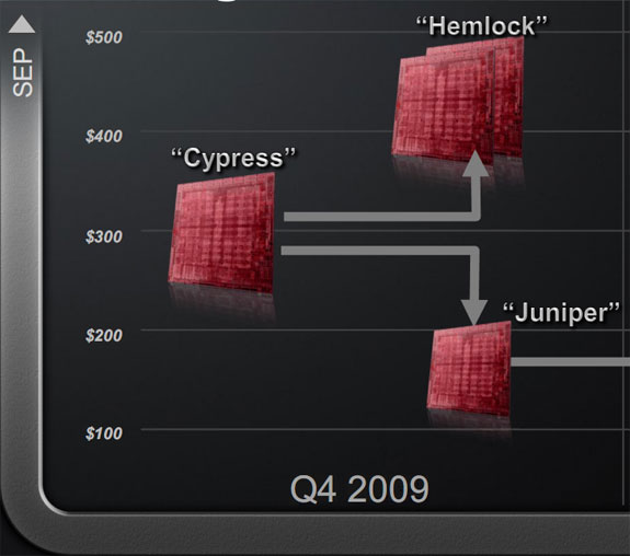
AMD PR would rather me refer to RV870 and the subject of today’s story as Cypress. The chart below shows AMD’s full listing of codenames for the 40nm DX11 GPU lineup:
| GPU | Codename |
| ATI Radeon HD 5900 Series | Hemlock |
| ATI Radeon HD 5800 Series | Cypress |
| ATI Radeon HD 5700 Series | Juniper |
| ATI Radeon HD 5600/5500 Series | Redwood |
| ATI Radeon HD 5400 Series | Cedar |
Given that we still haven’t purged the RVxxx naming from our vocabulary, I’m going to stick with RV870 for this story. But for those of you who have embraced the new nomenclature - RV870 = Cypress and at points I will use the two names interchangeably. The entire chip stack is called Evergreen. The replacement stack is called the Northern Islands.
TPS Rep...err PRS Documents
At ATI there’s a document called the Product Requirement Specification, PRS for short. It was originally a big text document written in Microsoft Word.
The purpose of the document is to collect all of the features that have to go into the GPU being designed, and try to prioritize them. There are priority 1 features, which are must-haves in the document. Very few of these get canned. Priority 2, priority 3 and priority 4 features follow. The higher the number, the less likely it’ll make it into the final GPU.
When Carrell Killebrew first joined ATI, his boss at the time (Dave Orton) tasked him with changing this document. Orton asked Carrell to put together a PRS that doesn’t let marketing come up with excuses for failure. This document would be a laundry list of everything marketing wants in ATI’s next graphics chip. At the same time, the document wouldn’t let engineering do whatever it wanted to do. It would be a mix of what marketing wants and what engineering can do. Orton wanted this document to be enough of a balance that everyone, whether from marketing or engineering, would feel bought into when it’s done.
Carrell joined in 2003, but how ATI developed the PRS didn’t change until 2005.
The Best Way to Lose a Fight - How R5xx Changed ATI
In the 770 story I talked about how ATI’s R520 delay caused a ripple effect impacting everything in the pipeline, up to and including R600. It was during that same period (2005) that ATI fundamentally changed its design philosophy. ATI became very market schedule driven.
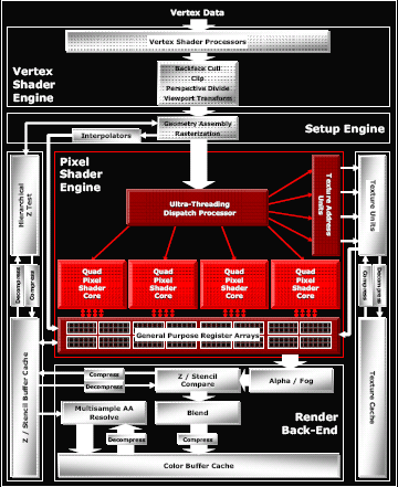
ATI's R520 Architecture. It was delayed.
The market has big bulges and you had better deliver at those bulges. Having product ready for the Q4 holiday season, or lining up with major DirectX or Windows releases, these are important bulges in the market. OEM notebook design cycles are also very important to align your products with. You have to deliver at these bulges. ATI’s Eric Demers (now the CTO of AMD's graphics group) put it best: if you don’t show up to the fight, by default, you lose. ATI was going to stop not showing up to the fight.
ATI’s switch to being more schedule driven meant that feature lists had to be kept under control. Which meant that Carrell had to do an incredible job drafting that PRS.
What resulted was the 80% rule. The items that made it onto the PRS were features that engineering felt had at least an 80% chance of working on time. Everyone was involved in this process. Every single senior engineer, everyone. Marketing and product managers got their opportunities to request what they wanted, but nothing got committed to without some engineer somewhere believing that the feature could most likely make it without slipping schedule.
This changed a lot of things.
First, it massively increased the confidence level of the engineering team. There’s this whole human nature aspect to everything in life, it comes with being human. Lose confidence and execution sucks, but if you are working towards a realistic set of goals then morale and confidence are both high. The side effect is that a passionate engineer will also work to try and beat those goals. Sly little bastards.
The second change is that features are more easily discarded. Having 200 features on one of these PRS documents isn’t unusual. Getting it down to about 80 is what ATI started doing after R5xx.
In the past ATI would always try to accommodate new features and customer requests. But the R5xx changes meant that if a feature was going to push the schedule back, it wasn’t making it in. Recently Intel changed its design policy, stating that any feature that was going into the chip had to increase performance by 2% for every 1% increase in power consumption. ATI’s philosophy stated that any feature going into the chip couldn’t slip schedule. Prior to the R5xx generation ATI wasn’t really doing this well; serious delays within this family changed all of that. It really clamped down on feature creep, something that’s much worse in hardware than in software (bigger chips aren’t fun to debug or pay for).
The Other Train - Building a Huge RV870
While the Radeon HD 5800 series just launched last September, discussions of what the GPUs would be started back in 2006.
Going into the fall of 2007 ATI had a rough outline of what the Evergreen family was going to look like. ATI was pretty well aware of DirectX 11 and Microsoft’s schedule for Windows 7. They didn’t know the exact day it would come out, but ATI knew when to prepare for. This was going to be another one of those market bulges that they had to align themselves with. Evergreen had to be ready by Q3 2009, but what would it look like?
Carrell wanted another RV770. He believed in the design he proposed earlier, he wanted something svelte and affordable. The problem, as I mentioned earlier, was RV770 had no credibility internally. This was 2007, RV770 didn’t hit until a year later and even up to the first day reviews went live there were skeptics within ATI.
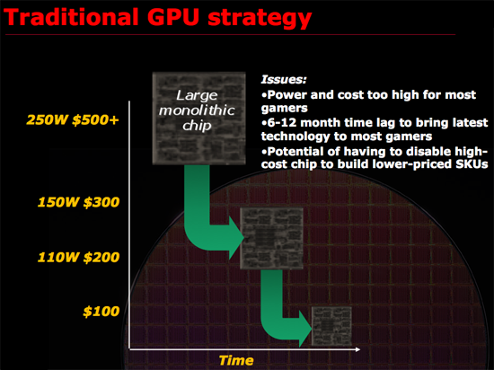
Marketing didn’t like the idea of building another RV770. No one in the press liked R600 and ATI was coming under serious fire. It didn’t help that AMD had just acquired ATI and the CPU business was struggling as well. Someone had to start making money. Ultimately, marketing didn’t want to be on the hook two generations in a row for not being at the absolute top.
It’s difficult to put PR spin on why you’re not the fastest, especially in a market that traditionally rewards the kingpin. Marketing didn’t want another RV770, they wanted an NVIDIA killer. At the time, no one knew that the 770 would be an NVIDIA killer. They thought they just needed to build something huge.
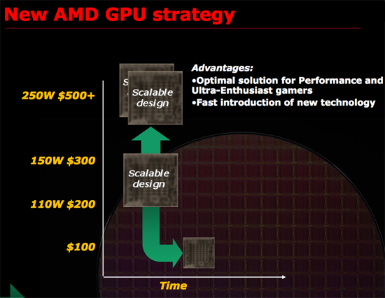
AMD's new GPU strategy...but only for the RV770
From August through November 2007, Carrell Killebrew came very close to quitting. The argument to build a huge RV870 because NVIDIA was going to build a huge competitor infuriated him. It was the exact thinking he fought so hard against just a year earlier with the RV770. One sign of a great leader is someone who genuinely believes in himself. Carrell believed his RV770 strategy was right. And everyone else was trying to get him to admit he was wrong, before the RV770 ever saw the light of day.
Even Rick Bergman, a supporter of Carrell’s in the 770 design discussions, agreed that it might make sense to build something a bit more aggressive with 870. It might not be such a bad idea for ATI to pop their heads up every now and then. Surprise NVIDIA with RV670, 770 and then build a huge chip with 870.
While today we know that the smaller die strategy worked, ATI was actually doing the sensible thing by not making another RV770. If you’re already taking a huge risk, is there any sense in taking another one? Or do you hedge your bets? Doing the former is considered juvenile, the latter - levelheaded.
Carrell didn’t buy into it. But his options were limited. He could either quit, or shut up and let the chips fall where they may.
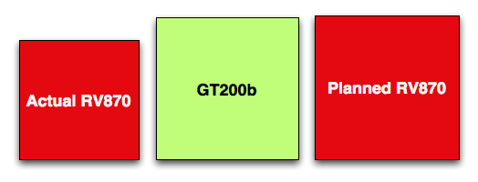
A comparison of die sizes - to scale.
What resulted was sort of a lame compromise. The final PRS was left without a die size spec. Carrell agreed to make the RV870 at least 2x the performance of what they were expecting to get out of the RV770. I call it a lame compromise because engineering took that as a green light to build a big chip. They were ready to build something at least 20mm on a side, probably 22mm after feature creep.
Adjusting Trajectory & Slipping Schedule
Carrell didn’t believe in building big chips anymore. It wasn’t that it was too difficult, it’s that it took too long for a $600 GPU to turn into a $200 GPU. AMD believed that the most important market was the larger (both in quantity and revenue) performance mainstream segment.
Rather than making the $200 - $300 market wait for new technology, Carrell wanted to deliver it there first and then scale up/down to later address more expensive/cheaper markets.
The risk in RV770 was architecture and memory technology. The risk in RV870 was architecture and manufacturing process, the latter which was completely out of AMD’s control.
Early on Carrell believed that TSMC’s 40nm wasn’t mature enough and that when it was ready, its cost was going to be much higher than expected. While he didn’t elaborate on this at the time, Carrell told me that there was a lot of information tuning that made TSMC’s 40nm look cheaper than it ended up being. I'll touch on this more later on in the article.
Carrell reluctantly went along with the desire to build a 400+ mm2 RV870 because he believed that when engineering wakes up and realizes that this isn’t going to be cheap, they’d be having another discussion.
In early 2008, going into Februrary, TSMC started dropping hints that ATI might not want to be so aggressive on what they think 40nm is going to cost. ATI’s costs might have been, at the time, a little optimistic.
Engineering came back and said that RV870 was going to be pretty expensive and suggested looking at the configuration a second time.
Which is exactly what they did.
The team met and stuck with Rick Bergman’s compromise: the GPU had to be at least 2x RV770, but the die size had to come down. ATI changed the configuration for Cypress (high end, single GPU RV870) in March of 2008.
And here’s where the new ATI really showed itself. We had a company that had decided to both 1) not let schedule slip, and 2) stop designing the biggest GPU possible. Yet in order to preserve the second belief, it had to sacrifice the first.
You have to understand, changing a chip configuration that late in the game, 1.5 years before launch, screws everything up. By the time RV770 came out, 870 was set in stone. Any changes even a year prior to that resets a lot of clocks. You have to go back and redo floorplan and configuration, there’s a lot of adjusting that happens. It takes at least a couple of weeks, sometimes a couple of months. It impacted schedule. And ATI had to work extremely hard to minimize that where possible. The Radeon HD 5870 was around 30 - 45 days late because of this change.
Remember ATI’s nothing-messes-with-schedule policy? It took a lot of guts on the part of the engineering team and Rick Bergman to accept a month+ hit on redesigning RV870. If you don’t show up to the fight, you lose by default, and that’s exactly what ATI was risking by agreeing to a redesign of Cypress.
This is also super important to understand, because it implies that at some point, NVIDIA made a conscious decision to be late with Fermi. ATI wasn’t the only one to know when DX11/Windows 7 were coming. NVIDIA was well aware and prioritized features that delayed Fermi rather than align with this market bulge. GPUs don’t get delayed without forewarning. AMD risked being late in order to make a smaller chip, NVIDIA risked being late to make a bigger one. These two companies are diverging.
The actual RV870
Engineering was scrambling. RV870 had to be a lot smaller yet still deliver 2x the computational power of RV770. Features had to go.
Carrell Loses His Baby: Say Goodbye to Sideport
Sitting at dinner with Eric Demers and Carrell Killebrew is honestly one of the best experiences I’ve ever had working with ATI. Before he got huge and subsequently left, I used to have annual dinners with Pat Gelsinger at Intel. They were amazing. To get to sit at the same table as someone as talented and passionate as a Gelsinger, Demers or Killebrew is one of the most fortunate and cherished parts of my job.
Eric was telling me about how they trimmed down 870 from over 400mm2 down to 334mm2 and how wonderful the end product was. I stopped him and asked for more detail here. I wanted an example of a feature that they had to throw out but they really wanted to keep in. Manufacturers rarely tell you what they threw out, marketing likes to focus on what’s in the chip and make everything sound like a well calculated move. Thankfully, marketing wasn’t allowed to speak at my dinner.
Eric turned to Carrell and said: “i know one feature we could talk about.”
“Sideport”.
Carrell responded, “OH MY GOD, that’s totally not fair.” (note that Carrell does not sound like a teenage girl, imagine that phrase just spoken more engineer-y).
When ATI first talked about the Radeon HD 4870 X2 they told us about a feature called Sideport. It was a port off each RV770 GPU that could be used for GPU-to-GPU communication.
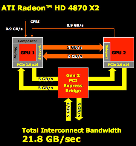
Sideport as it was intended to be used
The whole point of doing CrossFire in alternate frame rendering mode (AFR) is that the chips never have to talk. The minute you have to start synchronizing them, you kill performance. Sideport was supposed to alleviate that.
Unfortunately, due to power reasons, Sideport was never used on the 4870 X2. ATI’s reference design had it disabled and all vendors followed suit.
Sideport was Carrell Killebrew’s favorite feature, and he had to give it up.
In early 2008 ATI realized they had to cut this chip down from 20 - 22mm on a side to 18mm, everyone had to give up something. Carrell was the big advocate for making 870 smaller, he couldn’t be a hypocrite and not give anything up.
A bunch of my conversation with Carrell at this point had to go off the record. Sideport would have been useful in RV870, but it’s unfortunately not there. Although he did tell me not to be surprised if I saw Sideport again at some point. Carrell doesn’t give up easily.
What Made it All Ok: 4 GPUs in < 6 Months
Through a lot of hard work and sacrifice, even on Carrell’s part, ATI cut the RV870 from as much as 22mm on a side down to roughly 18mm x 18mm. The problem is that RV770 was around 16mm on a side. The RV870 was still too big.
Carrell wanted to cut it down even more, but two things changed his mind. First, in order to build 870 in the space of a 770 ATI would have to cut out much more from the chip than Carrell originally tought. One of the things that would have to go was some of the shader core.
In order to run the GDDR5 memory at the sort of data rates that ATI was targeting for the 5870 the analog PHYs on the chip had to grow considerably. At 16mm on a side ATI would either have to scale back memory bandwidth or eat into the shader core area. Either way we would’ve had a slower chip.
I asked Carrell if 16mm on a side would’ve made the RV870 $100 cheaper at launch, putting it on par with the RV770 launch prices. He said no. I didn’t find out why until much later, but I’ll save that story for another time.
Sacrificing performance to meet the 16mm x 16mm die size targets wasn’t going to happen, but what ultimately convinced Carrell to go with a larger die this time around was something that ATI didn’t get nearly enough praise for: the ability to launch 4 different 40nm DirectX 11 GPUs in less than 6 months.
Remember that Carrell’s beef with building the biggest GPU possible is that it takes too long for the majority of customers to get access to derivatives of that GPU. Look at how long it took G80 or GT200 to scale down. And who knows when we’ll see $150 Fermi/GF100 derivatives.
But ATI Engineering promised two things. First, that Cypress would have a successor called Juniper that would be ready around the same time. Secondly, two more GPUs would follow and the whole stack will be done and out in less than 6 months. ATI came close in 2008 with 3 GPUs in 3 months, but the fourth member of the 4000 series didn’t show up until April of 2009.
It wasn’t an impossible feat. ATI does have concurrent design teams and a lot of engineering resources in India/China. By working on Juniper in tandem with Cypress, assuming there were no show stopping bugs, ATI could exploit efficiencies in two teams effectively working on the same hardware (Juniper was just half a Cypress).
The idea of taking such a huge risk made Carrell uncomfortable. Running two GPU designs in parallel, for the same family of chips, is risky. If everything works out perfectly, you get two chips out at the same time. If it doesn’t, you’ve just tied up two design teams on one product generation. A slip here would give ATI its own Fermi.
What ultimately sold Carrell was the fact that engineering told him that they believed they could pull it off. Carrell believes in people. He believes if you expect the best out of those around you, then that’s what you’ll get. He couldn’t reconcile his beliefs with doubting the schedule engineering was feeding him. Carrell nervously signed off and the Evergreen stack was born.
Cypress and Juniper were delivered nearly at the same time. In fact, Juniper was ready a bit earlier and was sampled to developers months before ATI launched the 5000 series. Cedar and Redwood followed, not to mention a dual-Cypress board that became the Radeon HD 5970. And all of this was done and ready in less than 6 months (the chips themselves were all ready within 4 months).
When the smoke cleared ATI had new DirectX 11 parts at $600, $400, $300, $200, $150, $100 and $60. The Windows 7/DirectX 11 market bulge just got serviced.
The Cost of Jumping to 40nm
This part of the story could almost stand on its own, but it directly impacts much of what happened with Cypress and the entire Evergreen stack that it’s worth talking about here.
By now you’ve most likely heard about issues with TSMC’s 40nm process. While the word is that the issues are finally over, poor yields and a slower than expected ramp lead to Cypress shortages last year and contributed to NVIDIA’s Fermi/GF100 delay. For the next couple of pages I want to talk about the move to 40nm and why it’s been so difficult.
The biggest issue with being a fabless semiconductor is that you have one more vendor to deal with when you’re trying to get out a new product. On top of dealing with memory companies, component manufacturers and folks who have IP you need, you also have to deal with a third party that’s going to actually make your chip. To make matters worse, every year or so, your foundry partner comes to you with a brand new process to use.
The pitch always goes the same way. This new process is usually a lot smaller, can run faster and uses less power. As with any company whose job it is to sell something, your foundry partner wants you to buy its latest and greatest as soon as possible. And as is usually the case in the PC industry, they want you to buy it before it's actually ready.
But have no fear. What normally happens is your foundry company will come to you with a list of design rules and hints. If you follow all of the guidelines, the foundry will guarantee that they can produce your chip and that it will work. In other words, do what we tell you to do, and your chip will yield.
Global Foundries' 2010 - 2011 Manufacturing Roadmap
The problem is that if you follow every last one of these design rules and hints your chip won’t be any faster than it was on the older manufacturing process. Your yield will be about the same but your cost will be higher since you’ll bloat your design taking into account these “hints”.
Generally between process nodes the size of the wafer doesn’t change. We were at 200mm wafers for a while and now modern fabs use 300mm wafers. The transistor size does shrink however, so in theory you could fit more die on a wafer with each process shrink.
The problem is with any new process, the cost per wafer goes up. It’s a new process, most likely more complex, and thus the wafer cost is higher. If the wafer costs are 50% higher, then you need to fit at least 50% more die on each wafer in order to break even with your costs on the old process. In reality you actually need to fit more than 50% die per wafer on the new process because yields usually suck at the start. But if you follow the foundry’s guidelines to guarantee yield, you won’t even be close to breaking even.
The end result is you get zero benefit from moving to the new process. That’s not an option for anyone looking to actually use Moore’s Law to their advantage. Definitely not for a GPU company.
The solution is to have some very smart people in your company that can take these design rules and hints the foundry provides, and figure out which ones can be ignored, and ways to work around the others. This is an area where ATI and NVIDIA differ greatly.
Process vs. Architecture: The Difference Between ATI and NVIDIA
Ever since NV30 (GeForce FX), NVIDIA hasn’t been first to transition to any new manufacturing process. Instead of dedicating engineers to process technology, NVIDIA chooses to put more of its resources into architecture design. The flipside is true at ATI. ATI is much less afraid of new process nodes and thus devotes more engineering resources to manufacturing. Neither approach is the right one, they both have their tradeoffs.
NVIDIA’s approach means that on a mature process, it can execute frustratingly well. It also means that between major process boundaries (e.g. 55nm to 40nm), NVIDIA won’t be as competitive so it needs to spend more time to make its architecture more competitive. And you can do a lot with just architecture alone. Most of the effort put into RV770 was architecture and look at what it gave ATI compared to the RV670.
NVIDIA has historically believed it should let ATI take all of the risk jumping to a new process. Once the process is mature, NVIDIA would switch over. That’s great for NVIDIA, but it does mean that when it comes to jumping to a brand new process - ATI has more experience. Because ATI puts itself in this situation of having to jump to an unproven process earlier than its competitor, ATI has to dedicate more engineers to process technology in order to mitigate the risk.
In talking to me Carrell was quick to point out that moving between manufacturing processes is not a transition. A transition implies a smooth gradient from one technology to another. But moving between any major transistor nodes (e.g. 55nm to 45nm, not 90nm to 80nm) it’s less of a transition and more of a jump. You try to prepare for the jump, you try your best to land exactly where you want to, but once your feet leave the ground there’s very little to control where you end up.
Any process node jump involves a great deal of risk. The trick as a semiconductor manufacturer is how you minimize that risk.
At some point, both manufacturers have to build chips on a new process node otherwise they run the risk of becoming obsolete. If you’re more than one process generation behind, it’s game over for you. The question is, what type of chip do you build on a brand new process?
There are two schools of thought here: big jump or little jump. The size refers to the size of the chip you’re using in the jump.
Proponents of the little jump believe the following. In a new process, the defect density (number of defects per unit area on the wafer) isn’t very good. You’ll have a high number defects spread out all over the wafer. In order to minimize the impact of high defect density, you should use a little die.
If we have a wafer that has 100 defects across the surface of the wafer and can fit 1000 die on the wafer, the chance that any one die will be hit with a defect is only 10%.
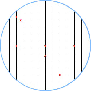
A hypothetical wafer with 7 defects and a small die. Individual die are less likely to be impacted by defects.
The big jump is naturally the opposite. You use a big die on the new process. Now instead of 1000 die sharing 100 defects, you might only have 200 die sharing 100 defects. If there’s an even distribution of defects (which isn’t how it works), the chance of a die being hit with a defect is now 50%.
A hypothetical wafer with 7 defects and a large die.
Based on yields alone, there’s no reason you’d ever want to do a big jump. But there is good to be had from the big jump approach.
The obvious reason to do a big jump is if the things you’re going to be able to do by making huge chips (e.g. outperform the competition) will net you more revenue than if you had more of a smaller chip.
The not so obvious, but even more important reason to do a big jump is actually the reason most don’t like the big jump philosophy. Larger die are more likely to expose process problems because they will fail more often. With more opportunity to fail, you get more opportunity to see shortcomings in the process early on.
This is risky to your product, but it gives you a lot of learning that you can then use for future products based on the same process.
The Payoff: How RV740 Saved Cypress
For its first 40nm GPU, ATI chose the biggest die that made sense in its roadmap. That was the RV740 (Radeon HD 4770):
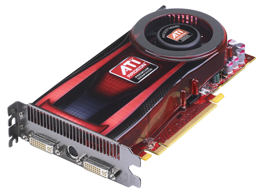
The first to 40nm - The ATI Radeon HD 4770, April 2009
NVIDIA however picked a smaller die. While the RV740 was a 137mm2 GPU, NVIDIA’s first 40nm parts were the G210 and GT220 which measured 57mm2 and 100mm2. The G210 and GT220 were OEM-only for the first months of their life, and I’m guessing the G210 made up a good percentage of those orders. Note that it wasn’t until the release of the GeForce GT 240 that NVIDIA made a 40nm die equal in size to the RV740. The GT 240 came out in November 2009, while the Radeon HD 4770 (RV740) debuted in April 2009 - 7 months earlier.
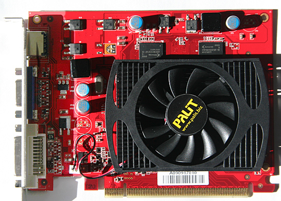
NVIDIA's first 40nm GPUs shipped in July 2009
When it came time for both ATI and NVIDIA to move their high performance GPUs to 40nm, ATI had more experience and exposure to the big die problems with TSMC’s process.
David Wang, ATI’s VP of Graphics Engineering at the time, had concerns about TSMC’s 40nm process that he voiced to Carrell early on in the RV740 design process. David was worried that the metal handling in the fabrication process might lead to via quality issues. Vias are tiny connections between the different metal layers on a chip, and the thinking was that the via failure rate at 40nm was high enough to impact the yield of the process. Even if the vias wouldn’t fail completely, the quality of the via would degrade the signal going through the via.
The second cause for concern with TSMC’s 40nm process was about variation in transistor dimensions. There are thousands of dimensions in semiconductor design that you have to worry about. And as with any sort of manufacturing, there’s variance in many if not all of those dimensions from chip to chip. David was particularly worried about manufacturing variation in transistor channel length. He was worried that the tolerances ATI were given might not be met.
![]()
A standard CMOS transistor. Its dimensions are usually known to fairly tight tolerances.
TSMC led ATI to believe that the variation in channel length was going to be relatively small. Carrell and crew were nervous, but there’s nothing that could be done.
The problem with vias was easy (but costly) to get around. David Wang decided to double up on vias with the RV740. At any point in the design where there was a via that connected two metal layers, the RV740 called for two. It made the chip bigger, but it’s better than having chips that wouldn’t work. The issue of channel length variation however, had no immediate solution - it was a worry of theirs, but perhaps an irrational fear.
TSMC went off to fab the initial RV740s. When the chips came back, they were running hotter than ATI expected them to run. They were also leaking more current than ATI expected.
Engineering went to work, tearing the chips apart, looking at them one by one. It didn’t take long to figure out that transistor channel length varied much more than the initial tolerance specs. If you get a certain degree of channel length variance some parts will run slower than expected, while others would leak tons of current.
Engineering eventually figured a way to fix most of the leakage problem through some changes to the RV740 design. The performance was still a problem and the RV740 was mostly lost as a product because of the length of time it took to fix all of this stuff. But it served a much larger role within ATI. It was the pipe cleaner product that paved the way for Cypress and the rest of the Evergreen line.
As for how all of this applies to NVIDIA, it’s impossible to say for sure. But the rumors all seem to support that NVIDIA simply didn’t have the 40nm experience that ATI did. Last December NVIDIA spoke out against TSMC and called for nearly zero via defects.
The rumors surrounding Fermi also point at the same problems ATI encountered with the RV740. Low yields, the chips run hotter than expected, and the clock speeds are lower than their original targets. Granted we haven’t seen any GF100s ship yet, so we don’t know any of it for sure.
When I asked why it was so late with Fermi/GF100, NVIDIA pointed to parts of the architecture - not manufacturing. Of course, I was talking to an architect at the time. If Fermi/GF100 was indeed NVIDIA’s learning experience for TSMC’s 40nm I’d expect that its successor would go much smoother.
It’s not that TSMC doesn’t know how to run a foundry, but perhaps the company made a bigger jump than it should have with the move to 40nm:
| Process | 150nm | 130nm | 110nm | 90nm | 80nm | 65nm | 55nm | 40nm |
| Linear Scaling | - | 0.866 | 0.846 | 0.818 | 0.888 | 0.812 | 0.846 | 0.727 |
You’ll remember that during the Cypress discussion, Carrell was convinced that TSMC’s 40nm process wouldn’t be as cheap as it was being positioned as. Yet very few others, whether at ATI or NVIDIA, seemed to believe the same. I asked Carrell why that was, why he was able to know what many others didn’t.
Carrell chalked it up to experience and recounted a bunch of stuff that I can’t publish here. Needless to say, he was more skeptical of TSMC’s ability to deliver what it was promising at 40nm. And it never hurts to have a pragmatic skeptic on board.
Preventing Espionage at AMD: How The Eyefinity Project Came to Be
There’s one more thing Carrell Killebrew has done for the world. He’s single handedly responsible for getting Eyefinity included in the Evergreen stack.
It started like this. All GPU vendors go to their customers (OEMs) and ask them for features they’d like to have. The notebook vendors wanted a total of 6 display outputs from the GPU, although they only needed two to be active at the same time. Two paths could be used for LCD panels, two could be used for external outputs (VGA + DVI/HDMI) and two routed to a docking station connector.
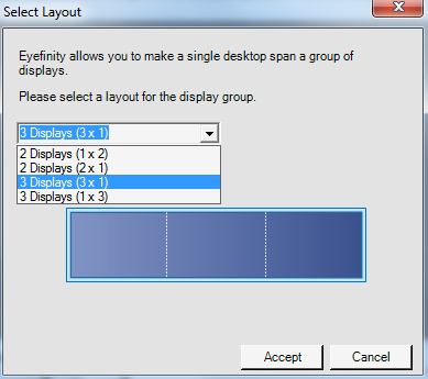
Carrell thought it would be a shame to have all of these output pins but not be able to drive all six at the same time. So he came up with a plan to be able to drive at least 3 displays on any Evergreen card. The high end cards would support 6 displays simultaneously.
His desire to do this wasn’t born out of pure lunacy, Carrell does have a goal in mind. Within the next 6 years he wants to have a first generation holodeck operational. A first generation holodeck would be composed of a 180 degree hemispherical display with both positionally and phase accurate sound. We’ll also need the pixel pushing power to make it all seem lifelike. That amounts to at least 100 million pixels (7 million pixels for what’s directly in front of you, and the rest for everything else in the scene), or almost 25 times the number of pixels on a single 30” display.
We’re not quite at 2016, so he had to start somewhere. And that somewhere happened to be with enabling a minimum of 3 and a maximum of 6 displays, per card, for all members of the Evergreen family. Today we know the technology as Eyefinity, but internally Carrell called it SunSpot.
Carrell didn’t want anyone knowing about SunSpot, so he kept it off the Cypress PRS. Through some very clever maneuvering he managed to keep it off of the radar while engineering hammered out the PRS, and even managed to keep it off of the chopping block when the GPU was cut down in size. He knew that if anyone got wind of it, they’d ask him to kill it while the chip was being scaled down. To make matters worse, if anyone outside of a trusted few became aware of it - there was the chance that NVIDIA would have time to copy and implement the feature. It then became Carrell’s goal to keep SunSpot as quiet as possible.
It began with a list. On this list were names of people who needed to know about SunSpot. If your name wasn’t on the list not only did you not know about SunSpot, but no one who knew about the project was allowed to talk about it near you. There was an internal website created that had the names of everyone who needed to know about SunSpot.
Along with the list, came rules.
As I just mentioned, no one on the list could talk about SunSpot in a place where someone not on the list could overhear. And if you wanted to get someone added to the list, it had to be approved - the final say was in the hands of none other than Carrell Killebrew.
The SunSpot engineers went to work on the feature, bringing in others only when absolutely necessary. The team grew one person at a time and eventually plateaued. The software engineers weren’t made aware of SunSpot until the last minute. Carrell only gave them enough time to enable SunSpot, they didn’t get the luxury of advance knowledge.
Carrell went to David Glenn, head of software engineering at ATI and asked him what the latest possible date that they needed to have someone in software working on this stuff. David gave him a date. Carrell asked for a list of names of people who needed to know. David gave him three names. On that date, the SunSpot team called up those three people and said “we need to tell you something”. Needless to say, no one was happy about Carrell’s secrecy. Some of the higher ups at ATI knew Carrell had people working on something, they just had no idea what it was.
It's the software that ultimately made Eyefinity
When in his own cube Carrell always spoke about SunSpot in code. He called it feature A. Carrell was paranoid, and for good reason. The person who sat on the other side of Carrell’s cube wall left to work for NVIDIA a couple months into the SunSpot project. In all, ATI had three people leave and work for NVIDIA while SunSpot was going on. Carrell was confident that NVIDIA never knew what was coming.
Other than the obvious, there was one real problem with Carrell’s secrecy. In order for Eyefinity to work, it needed support from external companies. If you’ll remember back to the Radeon HD 5800 series launch, Samsung announced thin-bezel displays to be sold in 1, 3 or 6 panel configurations specifically for Eyefinity setups. There was no way to keep SunSpot a secret while still talking to OEMs like Samsung, it’s just too big of a risk. The likelihood of someone within ATI leaking SunSpot to NVIDIA is high enough. But from an employee for an OEM that deals with both companies? That’s pretty much guaranteed.
For a feature like SunSpot to go completely unnoticed during the development of a GPU is unheard of. Carrell even developed a rating system. The gold standard is launch; if SunSpot could remain a secret until the launch, that’s gold. Silver is if they can keep it a secret until they get chips back. And the effort would get a bronze if they could keep it a secret up to tape out, at that point NVIDIA would be at least one full product cycle behind ATI.
Eventually, Rick Bergman, GM of graphics at AMD, committed to keeping SunSpot a secret until bronze, but he told Carrell that when they got to tape out they were going to have a serious talk about this.
Time went on, SunSpot went on, Carrell and crew made it to bronze. The chip had taped out and no one knew about Carrell’s pet project. It got a little past bronze and Rick asked Carrell to have that talk. There were three customers that would really benefit from talking to them about SunSpot, then the killer: it would also help ATI competitively.
Carrell didn’t want to risk tipping off the competition to SunSpot, but he knew that in order to make it successful he needed OEMs on board. The solution was to simply add those at the OEMs who needed to know about SunSpot to the list. The same rules applied to them, and they were given a separate NDA from existing NDAs in place between AMD and the OEM. AMD legal treated SunSpot as proprietary IP, if anyone else within an OEM needed to know about it they needed to first ask for permission to discuss it. To make sure that any leaks would be traceable, Carrell called SunSpot a different name to each of the three OEMs involved.
A few weeks prior to the Cypress launch one of the CEOs at one of the OEMs saw Eyefinity and asked to show it to someone else. Even the CEO’s request needed to be approved before he could share. Surprisingly enough, each of the three OEMs abided by their agreement - to Carrell’s knowledge the tech never leaked.
NVIDIA's Surround driven off two cards
While NVIDIA demonstrated its own triple-display technology at this year’s CES, it’s purely a software solution; each GPU is still only limited to two display outputs. I asked Carrell what he thought about NVIDIA’s approach, he was honest as always.
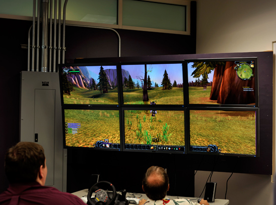
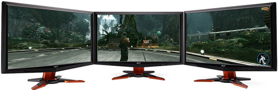
Eyefinity allows for 3 outputs from a single GPU
ATI considered a software only approach a while ago, but ultimately vetoed it for a couple of reasons. With the software-only solution you need to have a multi-GPU capable system. That means a more expensive motherboard, a more powerful PSU and a little more hassle configuration wise. Then there were the performance concerns.
One scenario is that you have very noticeable asymmetry as you have one card driving one display and the other card driving two displays. This can cause some strange problems. The other scenario is that you have all three displays coming off of a single card, and in alternating frames you send display data from one GPU to the next either via PCIe or a CF/SLI connector. With 6 displays, Carrell was concerned that there wouldn’t be enough bandwidth to do that fast enough.
There were also game compatibility concerns that made ATI not interested in the software approach. Although I was quick to point out that FOV and aspect ratio issues are apparent in many games today with Eyefinity. Carrell agreed, but said that it’s a lot better than they expected - and better than it would have been had they used a software-only solution.
Not to belittle the efforts of ATI’s software engineers here. While Carrell was one of three people originally responsible for SunSpot, they weren’t the ones who made it great. In Carrell’s own words “In the end, I’d say the most key contributions came from our Software engineering team. SunSpot is more a software feature than a hardware one”. ATI’s software team, despite not being clued into the project until it was implemented in hardware, was responsible for taking SunSpot and turning it into Eyefinity.
As for the ridiculous amount of secrecy that surrounded SunSpot? It wasn’t just to keep Carrell entertained. AMD has since incorporated much of Carrell’s brand of information compartmentalization into how it handled other upcoming features. I have to wonder if Carrell somehow managed to derive Apple’s equation for secrecy.
Final Words
Unlike a product review, there’s very little I can do to conclude here. There’s no buying recommendation, no performance to summarize. Even as an analytical piece there’s not much for me to conclude based on what I’ve learned at this point. When I wrote The RV770 Story I was convinced that ATI had embraced a new, refocused approach to GPU design, only to learn that they nearly threw out all of the learnings with the RV870.
The Northern Islands GPUs, due out later this year, were surely designed before anyone knew how RV870 would play out. Much less whether or not Fermi/GF100 would be this late.
I’m not sure any of what we’ve seen thus far in the history leading up to the RV770 or RV870 can tell us what we should expect from Northern Islands. While we can’t conclude about ATI’s future products, I do believe I have learned a considerable amount about how AMD’s graphics division works.
Carrell told me that the process of doing a product is not a logical process. There's logic in it, but it's not a logical process. It's an argumentative process. Not in the sense of having conflicts, but rather developing new data when the data isn't all there. When companies like AMD and NVIDIA do a product the engineers don't know all of the answers, and the knowledge they do have isn't binary - it's probability, it's weight, it's guesses. Sometimes they guess right, and sometimes they guess very wrong. The best they can do is to all weigh in with their individual experiences and together come up with the best group of guesses to implement. Over the years it seems that ATI has learned to, as much as possible, have all members of its team bought in to the product they're building.
The graphics team’s dedication and experience in jumping to new process technologies seems to have paid off with this generation. The move from TSMC to Global Foundries will surely challenge them once more. It’s not all about process technology though. The team’s focus on schedule and execution was a much needed addition to the company’s repertoire.
Carrell Killebrew helped turn ATI from a traditional GPU company with a poor track record, to one that could be known for its execution. The past three product generations have been executed extremely well. Regardless of whether you're an AMD, Intel or NVIDIA fan, you must give credit where it's due. The past couple of years have shown us a dramatic turn around from the graphics group at AMD. To go from the shakiness of the R500 and R600 GPUs to solidly executing on the RV670, 770 and 870 year after year is praiseworthy. I almost wonder if AMD’s CPU team could learn from the graphics group's execution. I do hope that along with the ATI acquisition came the open mindedness to learn from one another.


