Original Link: https://www.anandtech.com/show/2511
DFI X48 LT T2R: Floats like a Butterfly…
by Rajinder Gill on April 28, 2008 4:00 AM EST- Posted in
- Motherboards
After a very successful DFI P35 T2R motherboard launch, DFI endeavored to apply the same level of engineering expertise to Intel's X38/X48 chipsets. We did not review the DFI X38 motherboard, but instead decided to look at the X48-based motherboard from DFI in DDR2 form. Finally, after a slew of delays, Intel's X48 chipset is available in large enough quantities to manufacturers to allow full retail rollout. Intel delivered the initial batches of X48 chipsets to preferred launch partners such as ASUS and Gigabyte who were first to market, but now we are seeing this chipset in boards from other suppliers.
Expectations placed on the LANParty series from DFI are always high, but it has become more difficult for companies like DFI to stay ahead of the pack as boards from ASUS's ROG line have also begun to employ many of the additional BIOS functions that provided DFI with elite status among overclocking circles in the past. Although some of the competitors are now within a whisker of DFI's approach to BIOS options, a slight gap still remains in ultra fine voltage and memory clock skew control ranges; these allow users to dial in the last few MHz of stability while using lower levels of memory and chipset voltages (with some perseverance).
While this level of control to return ratio may not interest most users, DFI still enjoys a loyal following of people who regard tuning a DFI BIOS as a hobby and notable pastime. This does not mean that DFI's current boards only favor users who have vast levels of BIOS tuning experience or masses of time. In fact, DFI has improved the auto default settings of their boards considerably over the past year. So much so, that it is now no longer necessary to hold a masters degree in BIOS manipulation just to get the boards to boot and work in a stable manner. Online communities serve to provide additional information for those who are just starting out and want to learn more about the finer tweaking options that DFI provides.
In spite of DFI making these stock setting 'ease of use' advancements, we still have to concede that users of a 'tweaking' oriented mindset will lean towards this kind of motherboard. If instead you subscribe to the belief that all boards are the same, or if fine tweaking options do nothing to float your boat, there's a whole host of sub-$200 motherboards based on Intel's P35 chipset that fill the role of a good overclocking board perfectly. Boards priced above $200 must fight fiercely not only to provide masses of BIOS options and functionality, but also justification for their price tag against a competitively priced product. Ultimately, the boards are often so closely matched that winners emerge based upon the ease at which a user can attain high FSB speeds that can be run in a stable manner. The question is: can DFI topple ASUS's X38/X48 DDR2-based boards such as the Maximus Formula and superlative Rampage Formula?
 |
Interested to learn as much as we could about this X48-based offering, we spoke with DFI recently about their latest foray with Intel's chipsets. We were surprised to learn that Intel did not provide much support to DFI when it came to revealing the nature and use of performance related chipset registers that are available for manipulation via BIOS coding. So here, we have Intel claiming to be overclocking friendly on one hand and yet failing to provide full support to a key enthusiast manufacturer on the other. We are told this situation is set to improve - and rightly so. With rapid changes in processor architecture, B-tier manufacturers need all the support they can get to reduce development time and cut research costs in order to provide a competitive product in the market.
With release of Intel's P45 looming, DDR2-based X48 boards have their work cut out, especially if the P45 improves in areas such as low voltage requirements, reduced thermals, and tRD performance along with FSB overclocking headroom. If these conditions are met, a trump card of dual 16x PCIE slots on the X38/X48 chipsets may not hold enough allure to prevent users from looking at the P45, which can be simply teamed with any single slot dual-GPU solution to provide similar performance.
Reader feedback regarding our extensive BIOS guide on the DFI P35 UT T2R was very positive and we are back with a similar level of information today. Luckily, for us, the BIOS on the X48 board we are reviewing today bears many functional and naming similarities to the DFI P35 board - only the ranges really need changing, together with some additional work on the VTT/GTL reference voltage tables to get the most from it.
In keeping with our quest for continual improvement, we will present our first video BIOS setup guide that can be viewed easily if your computer has the latest version of Adobe's Flash Player loaded. We really feel that this will help users who have never used a DFI BIOS to obtain a reference point for setup when overclocking the latest dual-core CPUs from Intel. We will provide quad-core results shortly and look forward to your comments and suggestions with the new format. In the meantime, let's look at the DFI X48 LT T2R and see what this board offers for the enthusiast.
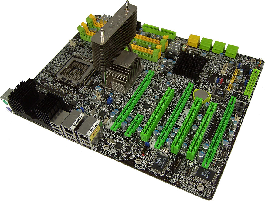
Board Layout and Features
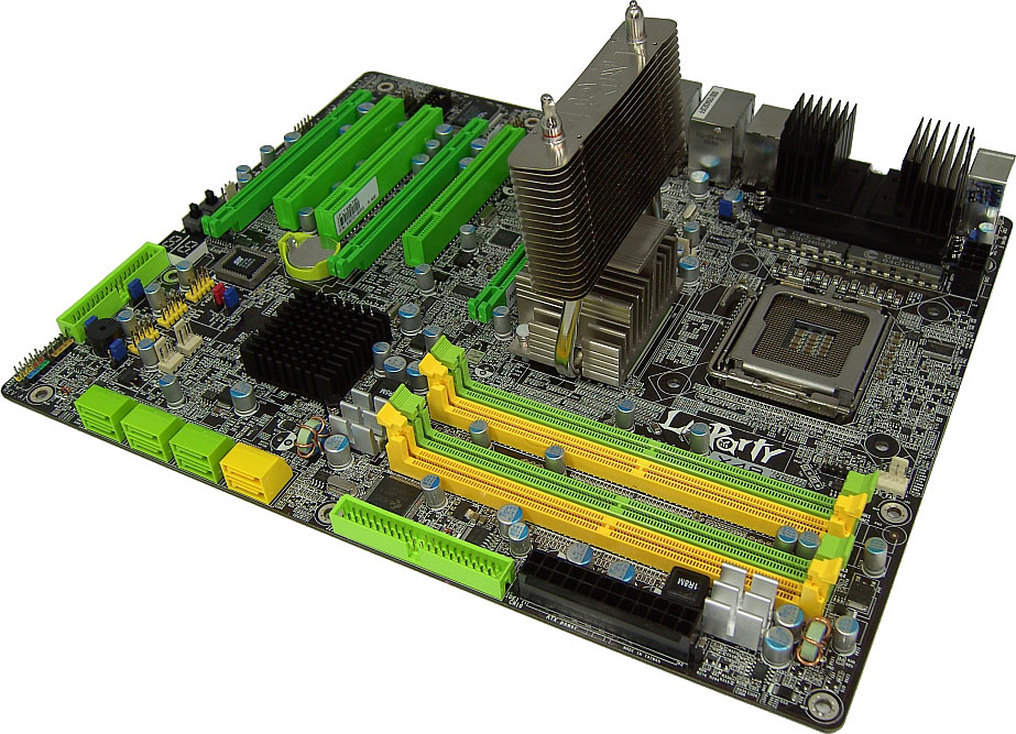 |
As with other LANParty boards, DFI's near-flawless layout continues. Cooling on the LT version is probably the best overall solution rather than opting for the upcoming UT version of this board, which connects all three heatsinks with a heatpipe. Having independent heatsinks allows users to replace a single section with more exotic cooling should they so desire, although we found that the stock Northbridge cooler (supplied by Thermalright) is very good. Teamed up with suitable airflow the Thermalright NB cooler is capable of dissipating large amounts of heat. Although we still recommend that active cooling is used on both the Northbridge and PWM area when overclocking this board.
Large CPU coolers like the Thermalright Ultra-120 must be mounted in horizontal orientation to provide clearance for the stock Northbridge cooler. This is not really a bad thing - using two 120mm fans in push-pull on the Thermalright 120 cooler will also cool the Northbridge heatsink very effectively. Using this combination of coolers with two 120mm fans in push-pull kept our full-load Northbridge temperatures under 42C even while using around 1.6VMCH.
We must stress that cooling the PWM heatsink is a little tricky when the board is mounted in a case. We used a small fan in combination with a couple of small machine screws to attach the fan to the PWM heatsink. We recommend that users monitor PWM load temperatures via the supplied ITE monitoring software and try to ensure that PWM temperatures remain around 50C under full load.
 |
All of DFI's performance oriented motherboards over the past year have featured 8-phase Volterra digital PWM circuitry to supply CPU power, and there's no change here. However, we would like to see the inclusion of a heatsink backplate on future DFI boards to ensure that the small Volterra MOSFETs do not lose contact with the heatsink when the motherboard bows under pressure from some of the higher torque mounting systems used on CPU coolers. As the Volterra MOSFETs are so small, any loss of contact between the FET and heatsink during a heavy transient load will result either in board shutdown or something catastrophic.
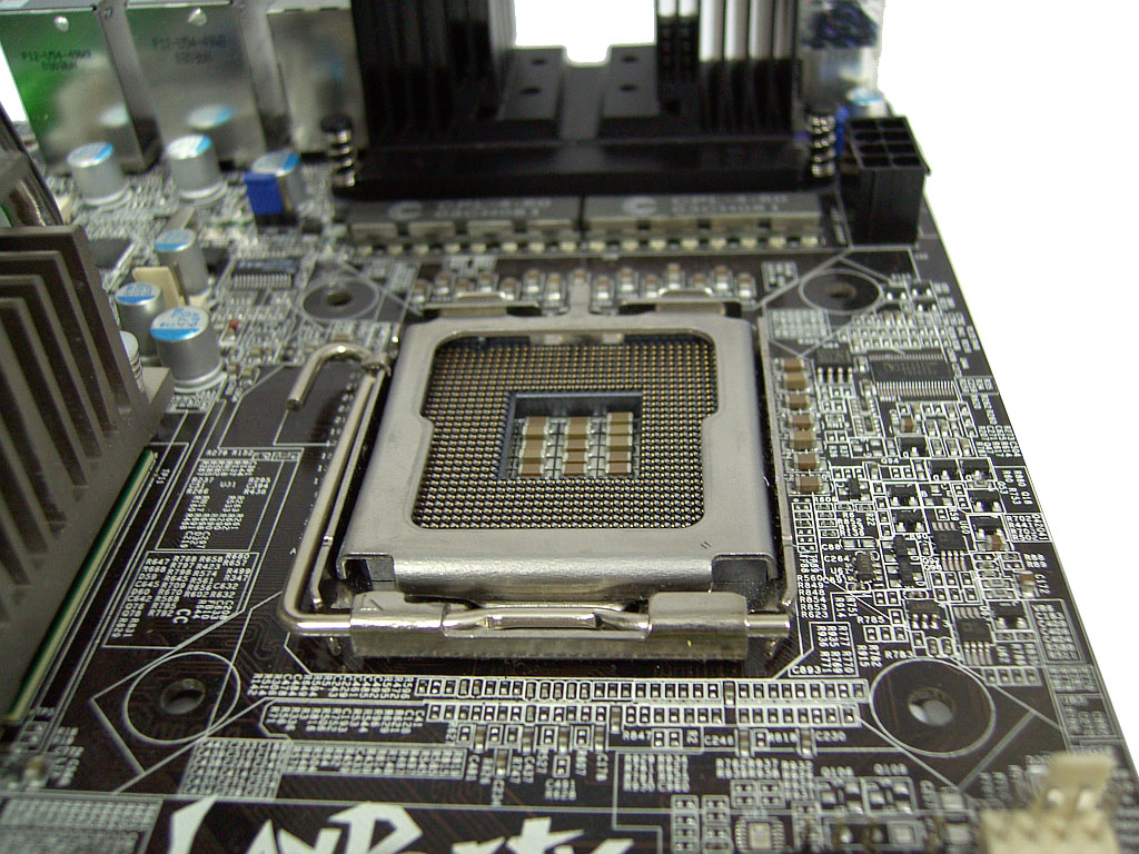
Even though we did not experience these problems ourselves, we feel the current implementation certainly has room for improvement. The EPS 12V power connector sits just behind the PS/2 ports at the top corner of the board, while the CPU fan header is situated adjacent to the first DIMM slot. There are six fan headers on the board - three of which are OS controllable via the supplied ITE monitoring software.
 |
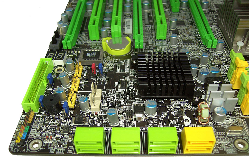 |
The overclocking friendly layout continues to an easily accessible CMOS battery, and onboard power and reset switches featuring EZ CMOS clear and of course the LED POST Code display. The floppy drive connector sits at the lower edge of the board to the right of the POST Code display. The six Intel ICH9R SATA ports are located at the lower right edge of the board, facing to the right making connector insertion a tad awkward at once the board is mounted in a case. There are also two JMicron JMB363 SATA ports situated above the Intel SATA ports.
The memory slot connectors are situated almost in line with the primary PCI Express connector; large graphics cards such as the 8800 GTX may have to be removed when swapping out memory modules. The 24-pin ATX connector is placed to the right of the slots and does not hinder the use of the IDE connector below it.
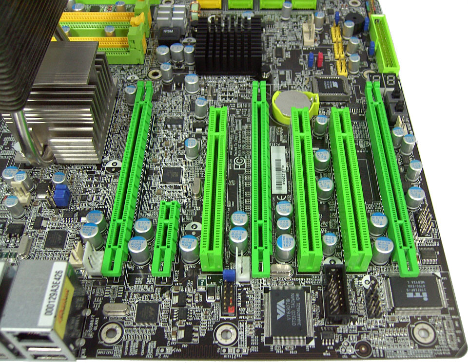 |
The expansion slot layout is comprised of three PCI Express x16 full length slots (two x16 bandwidth and one x4 bandwidth slot), one PCIEx1 slot, and three PCI slots. The supplied Bernstein Audio module features the Realtek ALC885 8-channel High Definition Audio CODEC and has its dedicated connector placed between the PCI slots, rendering one of the PCI slots inactive if the module is used. There are three onboard USB connectors for an additional six USB ports, a connector for an external COM port, one IrDA connector, one CIR connector, and a connector for the second IEEE-1394 port.
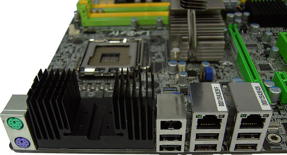 |
The rear I/O options include six USB ports, an IEEE-1394a port, two Gigabit LAN ports with teaming options, and finally the standard PS/2 keyboard and mouse ports.
Test Setup
|
DFI X48 LT T2R Standard/Overclocking/Benchmark Testbed |
|
| Processor | Intel E8500, 1333FSB 9X Multiplier, Intel QX9650 Quad CPU, 12MB Cache, 1333FSB Unlocked multiplier - 9X Default |
| CPU Voltage | 1.200V ~ 1.450V |
| Cooling | Air Cooling Thermalright Ultra 1200 using 2x Noctua NF-P12 120mm fans |
| Power Supply | PCP&C1200W |
| Motherboard | DFI X48 LT T2R |
| Memory | OCZ Reaper-X 1000MHz 2X2GB kit, OCZ Platinum XTC PC2 8000 2x2GB, OCZ Flex 9200 4X1GB |
| Memory Settings | Various - as shown |
| Video Cards | ASUS 8800 GTS 512 G92 - Underclocked to match Nvidia base clock levels for test comparison to 790/X48 chipset board scores |
| Video Drivers | 169.28 Drivers (Vista 64-bit) |
| Hard Drive | Western Digital 7200RPM 250GB SATA 3/Gbps 16MB Buffer |
| Optical Drives | Plextor 755A, Toshiba SD-H802A |
| Case | Lian-Li V-2110 |
| BIOS | Lttest |
| Operating System | Vista 64-bit SP1 |
| . | |
With such a vast array of overclocking BIOS functions at our disposal, a decision was made to stick with a single operating system environment. We feel Vista 64-bit has approached a level of maturity that eliminates the possibilities of OS-level conflicts, allowing us to spend time pushing the motherboard without fear of not being able to diagnose issues.
A majority of the benchmarks were run using an E8500 processor; our QX9650 gave up the ghost during testing. However, we still mustered enough experience with the QX9650 to find its sensible limits and provide users with our BIOS setup experience using this processor.
Both high-resolution 1920x1200 and 1280x1024 resolution game benchmark tests were run to find performance benefits for gamers, should such advancements through BIOS tweaking exist. We utilize new drive images on each board in order to minimize any potential driver conflicts. Our 3DMark results are generated utilizing the standard benchmark resolution for each program. We run each benchmark five times, throw out the two low and high scores, and report the remaining score.
Recent reviews of 780i, 790i, and X48 boards have allowed us to compile benchmark results in comparison to scores using the ASUS Striker II Extreme and ASUS P5E3 Premium and ASUS Striker II Formula. This gives us the chance to look at single card results from three different chipsets running either DDR3 or DDR2 memory. It's no surprise that things will be close, as most of us already know that memory bandwidth and speed typically only makes a 1-3% difference between DDR2 and DDR3 boards.
Synthetic Memory Performance
Memory access latency
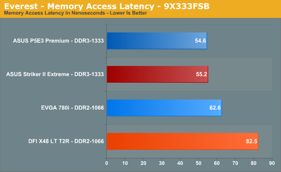
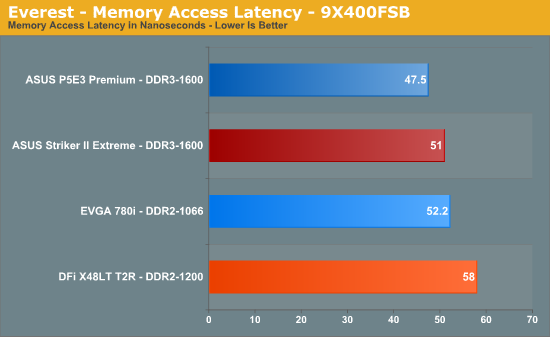
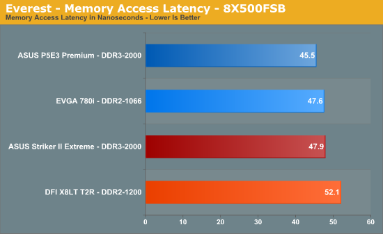
The DFI X48 does give up some access latency performance at 500FSB due to the inability of the board to run a flat tRD of 8 at 500FSB. We had to apply a tRD of 8, with some of the tRD phase registers pulled low to a tRD of 7. However, final judgment should rest upon how the board fares in other benchmarks that stress memory and PCIE transfer thoroughly over sustained periods.
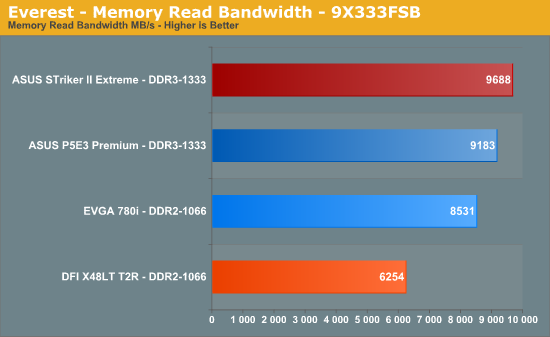
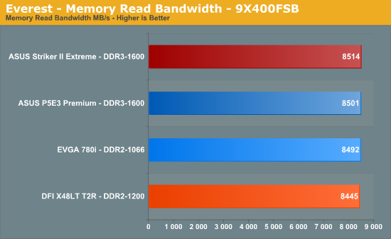
Memory Read Bandwidth

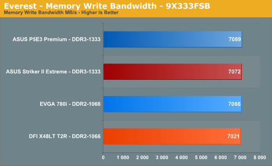
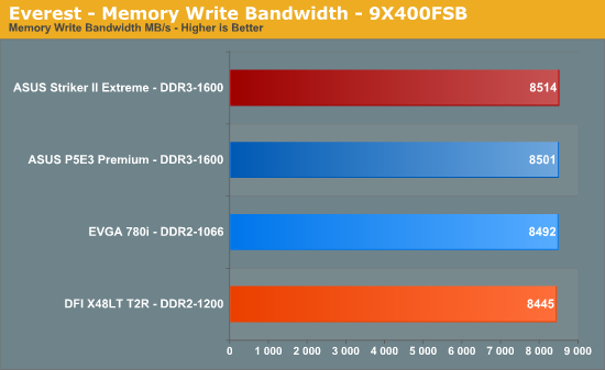
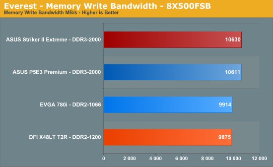
Memory Write Bandwidth
Memory Copy Bandwidth
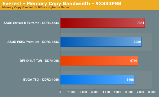
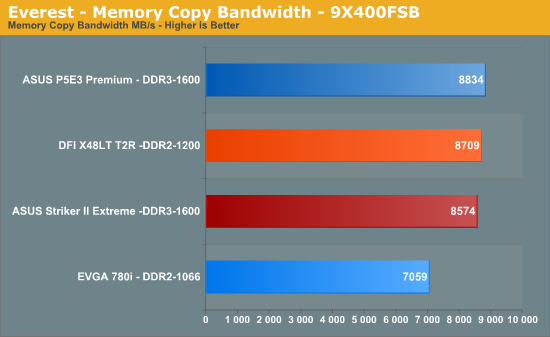
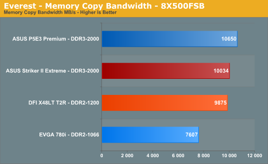
Even with the use of a high divider for 1200MHz memory speed at 3.6 and 4 GHz processor speeds, the DFI X48 cannot compete with the memory read bandwidth of the 780i reference board from EVGA. We tried all manner of BIOS performance adjustments. Standard tRD levels of 7 or 5 are unavailable at 400FSB and 500FSb respectively, hindering the synthetic figures somewhat. Copy and Write speeds are certainly competitive with the other boards though, but the overall picture is not impressive for a tweaker's board; we have seen DDR2-based X48 boards that do better.
Synthetic Graphics Performance
The 3DMark series of benchmarks developed and provided by Futuremark are among the most widely used tools for benchmark reporting and comparisons. Although the benchmarks are very useful for providing apples-to-apples comparisons across a broad array of GPU and CPU configurations, they are not a substitute for actual application and gaming benchmarks. In this sense, we consider the 3DMark benchmarks to be purely synthetic in nature but still valuable for providing consistent measurements of performance.
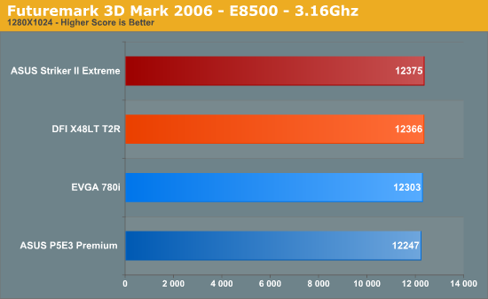
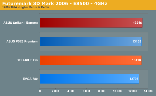
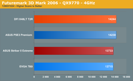
3DMark06 is almost completely oblivious to memory bandwidth and access latency, relying rather on raw GPU power and PCIE data transfer rates. In DDR2 format the X48 chipset keeps its nose ahead of the 780i-based motherboards with an E8500, while the QX9770 4GHz result hauls itself clear of the whole bunch. We still feel users will be more interested in how well the DFI board fares in actual games.
Crysis
Without doubt, Crysis is the sternest 3D test for any motherboard and GPU solution. The Crysis team reached new heights in developing a FPS engine that brings even the highest specification systems to their knees. Users have begun to base purchasing decisions solely on how well a component handles this game. As we are using a single card here, we have to stick with medium detail levels. Further, we are still experiencing problems with consistent benchmark results from the 64-bit version of the game, so we have to stick with running our benchmarks on the 32-bit version for now.
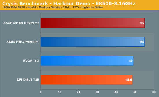
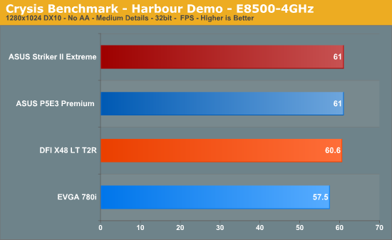
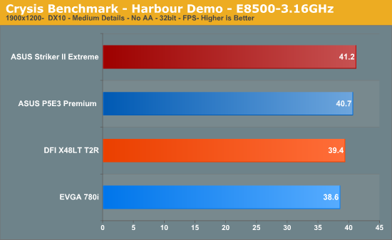
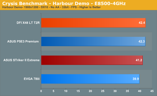
Like 3DMark06, Crysis is all about GPU power and PCIE bandwidth. Due to the nature of the Crysis 3D engine, the DFI X48 holds its own in Crysis and provided trouble free operation at stock and overclocked settings.
Unreal Tournament 3
The highly anticipated Unreal Tournament 3 landed on our PC's hard drive a while ago and has not failed to deliver the ultra fast FPS shooter we all expected. A slick 3D engine that provides ultra fast-paced action requires a system capable of sustaining frame rates during periods of intense online gaming action. Unlike other modern 3D gaming engines, Unreal's code is sensitive to memory performance and notable gains can be realized from tweaking memory bandwidth and chipset performance levels.
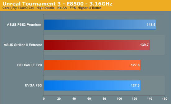
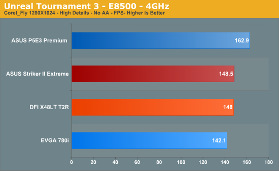
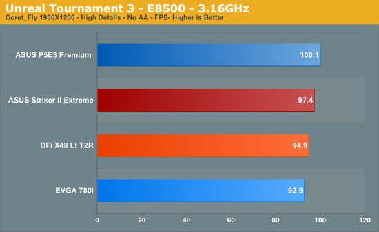
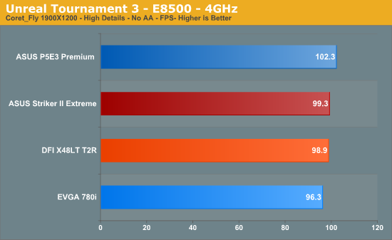
The DFI board performs admirably in UT3 when pitched against the EVGA 780i reference board. There really is no better solution for this game than a DDR3 system, but considering the price to performance ratio of the DDR2 boards, these scores are not bad at all for DFI.
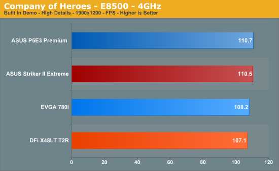
Company of Heroes
Despite having been around for a while, Company of Heroes is still one of the best strategy games available. The game is heavily GPU limited but also requires brute CPU processing power to keep things smooth during heavy action. The built-in benchmark is very responsive to GPU as well as CPU scaling, hence we think it provides good insight into overall system gaming power.
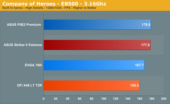
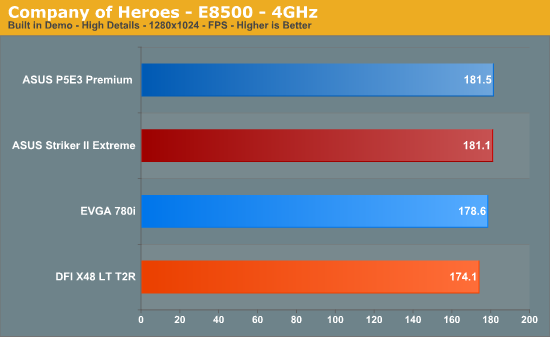
DFI scores lower at stock speeds due to the very loose default BIOS settings the board employs. At 4 GHz, the results are a little closer; either way the frame rates of all the boards should ensure solid game play at these settings. Actually, we could not notice any difference in game play between the boards at stock or overclocked settings. At these frame rates, one board scoring better than the other really does not make any difference unless you like showing off for others.
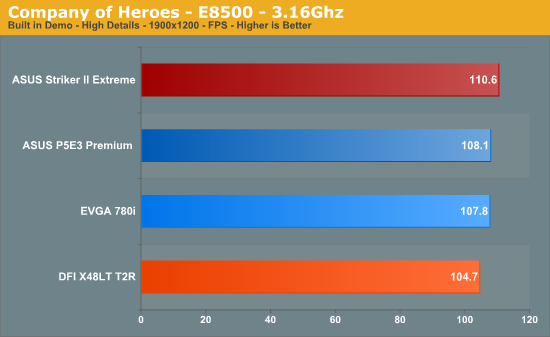
DFI's board falls behind EVGA across the range of testing at higher resolutions - certainly not in an excessive manner, but a victory certainly would have been more inspiring. Having benchmarked the board through a variety of tests, if squeezing performance is important to you, a wiser operating point will undoubtedly come at 450FSBX9 on the DFI board - if you find you can get away with a tRD of 6 or so. At 500 FSB, the board will not run a value of 7, which may have helped the scores by a few FPS here and there.
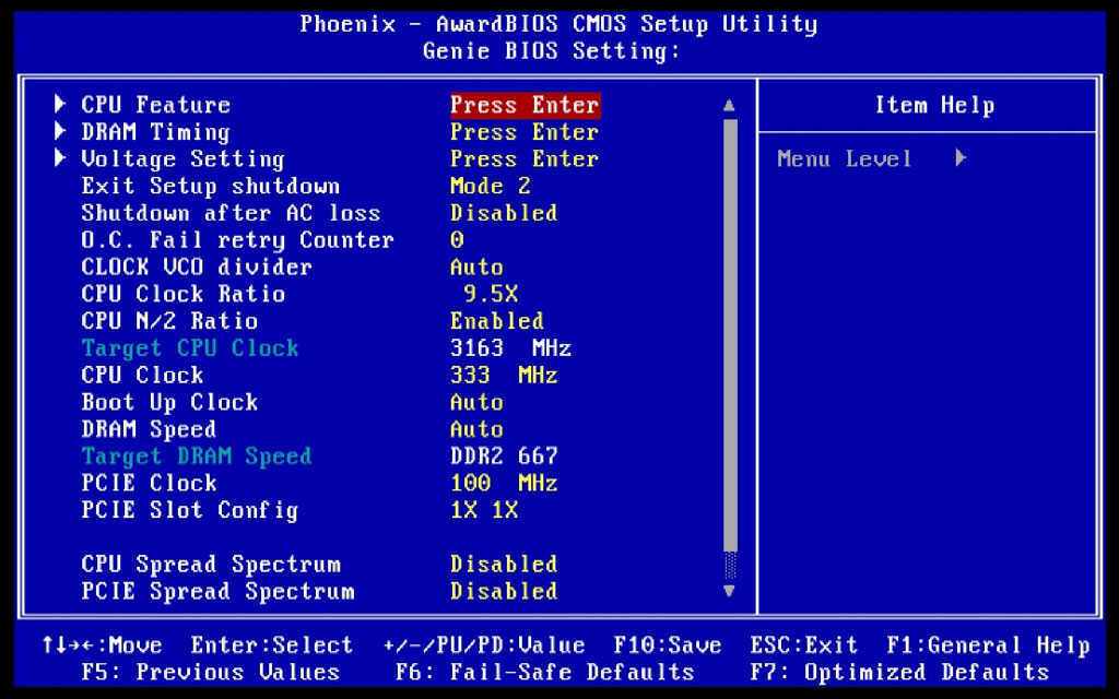
Important Performance Related BIOS Options
DFI supplied us with their latest BIOS for testing, which is set to go live sometime this week in a public beta. There are six new options for MCH termination and reference voltage adjustments. Three of the new settings over-complicate the BIOS to the point of being unnecessary so will probably be dropped for the public beta. The remaining three BIOS functions will be documented in this guide with the little information we have - even DFI is unsure as to their true nature and Intel has not been forthcoming with the information, shrouding these settings in further mystery.
For the most part, please note that we have decided to work on explanations of BIOS settings we deem worthy of user adjustment when overclocking. Settings we have left out were found to function adequately at the default/AUTO settings.
Genie BIOS Setting
 |
Boot Up Clock: Sets a safe user selected FSB speed for the system to revert to when an overzealous overclock fails.
PCIE Clock: Overclocking the PCIE bus can be useful for benchmarking, bringing small gains to overall scores. Unfortunately the X48/ICH9R combo does not have the potential for overall MHz we find with NVIDIA's 680i chipset which could run PCIE frequencies in excess of 150MHz for benchmarking. Generally, speeds below 110 MHz are safe enough to use, while SATA detection begins to fail when frequency is increased above 115MHz.
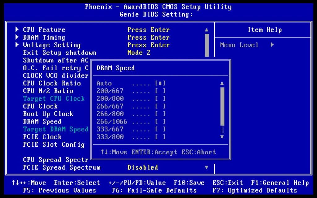
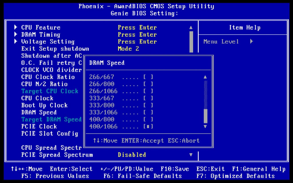
DRAM Speed
Available options are for this function can be seen in the following images:
 |
 |
We recommend that users with quad-core processors stay around 400FSB if they have the luxury of an unlocked multiplier. A 10x multiplier used at 400FSB will not require any GTL reference voltage adjustments to work and choosing the 266 strap will select a default tRD of 6 with some of the phases pulled down to 5 automatically in the BIOS. It really cannot get any simpler to set up one of these processors.
In fact, there are not any boards we know of that can quite eclipse this feat with 8GB of memory in place. We managed to run our board at default VMCH (1.25V) with a QX9650 and no less than 8GB of memory running DDR2-1000 and it was completely stable. Trying to beat this level of performance in any other way with 12MB cache quad-core CPUs is virtually impossible on this board. A default VTT voltage will get you close to 420 FSB, at which point a tRD adjustment as well as non-linear VTT increases for every 10FSB will follow.
We managed to get to 440FSB fully stable, but the VTT required was hardly safe for 24/7 use. As rule of thumb, do not exceed 1.34V (real), unless you have sub-zero cooling and are only running the board to perform a few benchmarks.
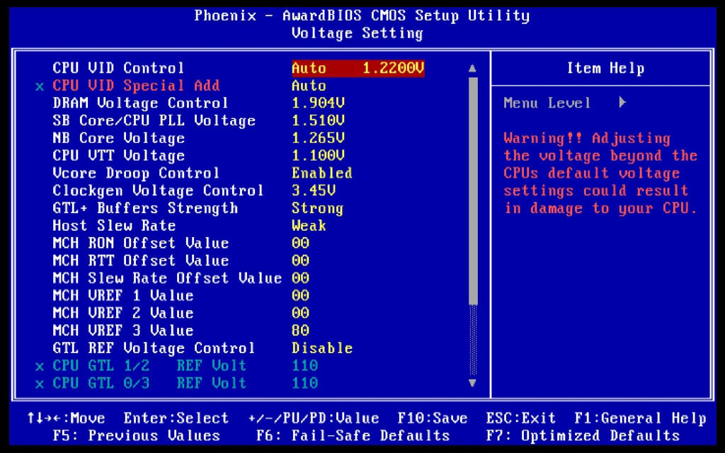 |
CPU VID Control: This function sets the current CPU Vcore (range from 0.8V to 1.6V); this function can be used in conjunction with "CPU VID Special Add", for overvolting past 1.6V if required.
CPU VID Special Add: Used in conjunction with "CPU VID Control", sets a percentage of VCore over the applied voltage using the "CPU VID Control" function; maximum is 125% over 1.6V.
VCore Droop Control: We generally leave this function to its default setting of Enabled. Using Enabled here ensures that the applied VCore is never compromised by overshoot while the PWM circuit is recovering for a heavy transient load. Disabling this function will remove the droop but will also strain the MOSFETs as they struggle to maintain the applied Vcore level, which fluctuates thousands of times a second from the applied value even in light load conditions. The recovery process with no Voffset usually results in longer settling times, which actually gives rise to instability in certain cases - a BSOD during the windows load process is a classic example of this at work.
NBCore Voltage: Sets the core voltage for the MCH. For quad-core CPUs, operating under 420FSB may require nothing more than 1.32V. Over 430FSB, the VMCH requirement rises quite drastically, making the whole process futile - especially when we consider that a rather loose tRD value is required just to hold the board stable. For dual-core processors, if properly tuned the VMCH requirement can be as low as 1.4V for benchmarking while full stability will need circa 1.55V. A properly tuned NBGTL reference voltage value, VTT, and MCH reference values all serve to reduce the requirement of higher levels of VMCH. Anything over 510FSB using a 45nm processor will require in excess of 1.6V though.
CPU VTT Voltage: VTT is the termination voltage used to string data lines between the CPU FSB and the MCH. Increasing this voltage usually enables FSB frequency to be increased. Both 65nm and 45nm processors can benefit from a slight overvolt, bearing in mind that GTL voltage values must be tuned effectively any time an adjustment is made to VTT. For 65nm dual- and quad-core processors we recommend that users attempt to overclock their systems without any adjustment to VTT and GTL and see how far the board will clock.
We have heard of instances where pushing 65nm quad-core processors to their internal FSB limits before any adjustment of VTT/GTL is necessary when using this board. For 45nm quad-cores, we have already outlined our thoughts on the sensible operating point at the beginning of this guide, which just so happens to not require any adjustment to VTT or GTL values.
Pushing dual-core 45nm processors requires no real adjustment to VTT or GTL right up to 485FSB on our board. After this point, we find that although we can run VTT levels in the region of 1.18-1.28V to benchmark the board, heavy CPU loads result in a system freeze irrespective of GTL tuning until we raise VTT to around 1.34V (real) and set GTL reference values in the region of 61% of VTT. The bottom line here is that many users should never need to alter VTT/GTL levels unless they happen to have Satan's donkey for a processor or are shooting for high FSB levels for their particular processor class.
MCH Vref 1/2/3 Value
The defaults for these three settings are 00/00/80. DFI informed us that all three settings must be moved in unison, i.e. the ratio between all three settings should be maintained if making any adjustments. Up to 500 FSB, adjustment of these three settings is not usually necessary (though the FSB threshold for required adjustment may be lower for quad-cores). Unfortunately, there is little information available to us as to exactly which part of the MCH is driven by these reference voltages.
However, through some fiddling, we have found that a value of 30/30/B0 works quite well on our board once beyond 500FSB with a 45nm dual-core CPU. Effects can be marginal at times and at others provide the MCH with enough offset to boot into the OS and allow a benchmark to run. With a hexadecimal scale ranging from 00 to FF, the permutations for adjustment are almost limitless.
We found values over 40/40/C0 did not provide us with any additional gain. Properly set, the ability of the board to run low levels of VMCH may become apparent for those who run just benchmarks. We managed to 3D benchmark our board right down at 1.4VMCH at 500FSB and 4GHz with an E8500 CPU with 4GB of memory when this setting was tuned for our board and parts combination, something we have not be able to do on any other X48 board in DDR2 form.
Toe to Toe with the BIOS (cont'd)
 |
 |
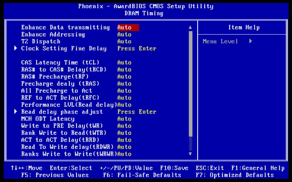
Regardless of individual memory timing preferences, to obtain best RAM/chipset latency performance we recommend that the following BIOS functions be set as follows for Micron D9-based RAM modules.
Enhance Data Transmitting: FAST
FAST MODE: Gives latency and bandwidth improvements over the "Normal" setting without overly affecting memory stability or FSB overclocking potential throughout the frequency ranges of interest for everyday use.
TURBO MODE: More suited to benchmarking runs. This is a very aggressive setting, further improving latencies past "Fast" mode. Using "Turbo" mode may require that the "CH1CH2 Common CLK Crossing Setting" be set to "Nominal" rather than "More Aggressive". VNB requirements are 1.7V and upwards, hence this should be used strictly for short-term benchmarking.
Enhance Addressing: FAST
This brings additional gains of latency and bandwidth used in combination with the above setting for best overall system performance. Again, the stability/voltage requirement hit is only minor for normal PC use. Although the BIOS defaults to Normal mode for both settings, there is no reason to veer away from setting FAST for both functions, provided you're using reasonable memory.
T2 Dispatch: Set this to Disabled, as it gives more overall stability when memory is clocked to high speeds.
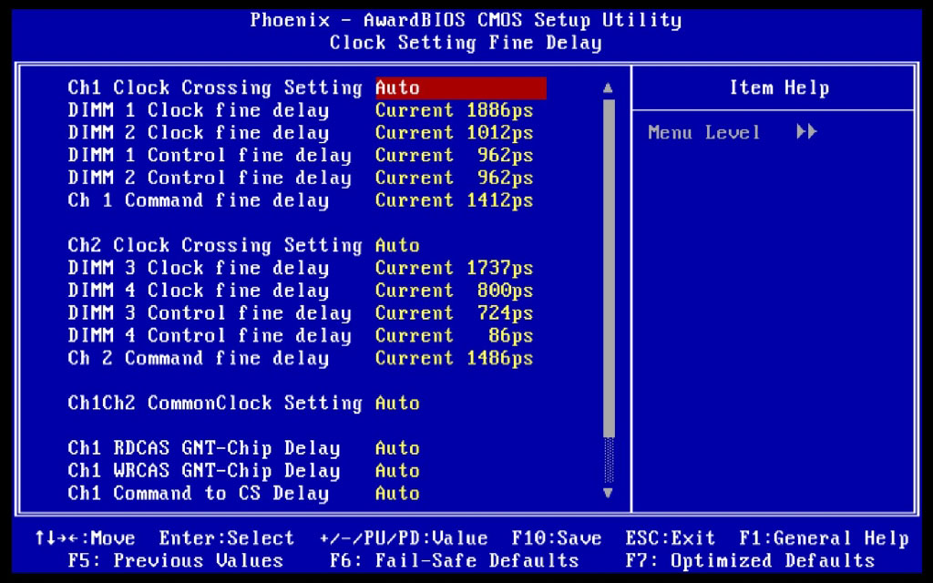 |
Channel 1 CLK Crossing Setting: More Aggressive
Channel 2 CLK Crossing Setting: More Aggressive
CH1CH2 Common CLK Crossing Setting: More Aggressive
24/7 systems using Micron D9GMH-based modules will certainly want to take advantage of using all three of these settings in unison for a latency and bandwidth boost. We have found these three functions set to "More Aggressive" do not hinder the boards FSB progress excessively. Other RAM modules may not fare as well, unfortunately. Given the choice between a hike in tRD (performance level) or setting the clock crossing settings less aggressively, always strive to maintain the lowest tRD possible. Taking a hit in the clock crossing setting is not as drastic as additional clock delays to the tRD transfer cycle.
Clock Fine Delays: For both channels, the BIOS adjusts these values automatically when set to CURRENT mode. The scale runs in picoseconds of delay for each setting/channel. Generally, engineers do a very good job of ensuring PCB trace lengths to each DIMM slot on the motherboard are of equal length. Slot 4 is around 3 cm or so from slot 1, so the traces running to DIMM slot 1 will often be "snaked" back across themselves in a U shape to add length to the trace and help eliminate parasitic capacitance issues when running two traces in parallel. The delay functions offer adjustment to help eliminate trace length mismatches ensuring data requests from the MCH are received and dispatched in unison when requested from the appropriate DIMM banks.
Although the BIOS does an admirable job of sensing the delay values required, we found that pushing the board requires some manual tuning of these settings. The Control Fine Delay values for each channel can often be left at Current, while tuning the Clock Fine Delay and Command Fine Delay Settings for both channels is certainly fruitful (depending also on which DIMM slots are occupied by modules). For the most part the delay in picoseconds between each bank should not exceed 70ps or so. Command Fine Delay seems to function best when set to around a 50% value of Clock Fine Delay.
The best way to monitor these settings is to write down the values at default (Current), if the board is stable. As you increase the FSB and hence change the memory frequency, the current values tend to drift away from their ideal or stable settings. To get around this, users can manually apply the settings shown for a stable overclock and tune the board for better stability by making small adjustments to the manually applied values. Do note however, that the values shown by the current settings are not available in the manual adjustment scale, so we must pick the closest value.
At times, the BIOS may select a Command Fine Delay setting that is wholly inadequate for the frequency applied. Often a value under 100ps may be selected, resulting in the board failing to boot into the OS, simply setting this value back to near 50% of the Clock Fine Delay value of Channel 1&3 often results in a "fix".
Performance Level
Leaving this function set to Auto works okay as long as the board is not going to be pushed. One of the issues pertaining to the current BIOS is that the BIOS automatically applies tRD Phase shifts (see the AUTO section below), which prevent the user from running a flat Performance Level unless a value is selected 1 higher than the required value and all the Phase Shift Registers (at least the active ones according to the memory divider) are set to Enabled. So, if you want to run a Performance Level of 7, select 8 and then proceed to set all the tRD Phase shift registers to Enabled, which will in fact give you a tRD of 7.
If the registers are left at AUTO, there's a good chance that the board will fail to POST at higher FSB speeds that happen to fall at the limit of the applied level of tRD. For example if the limit of tRD 6 happens to be at 450 FSB and tRD phase shifts are left to AUTO, some of the channels will pull down to a tRD of 5 resulting in either a non-POST or a system hang during OS loading.
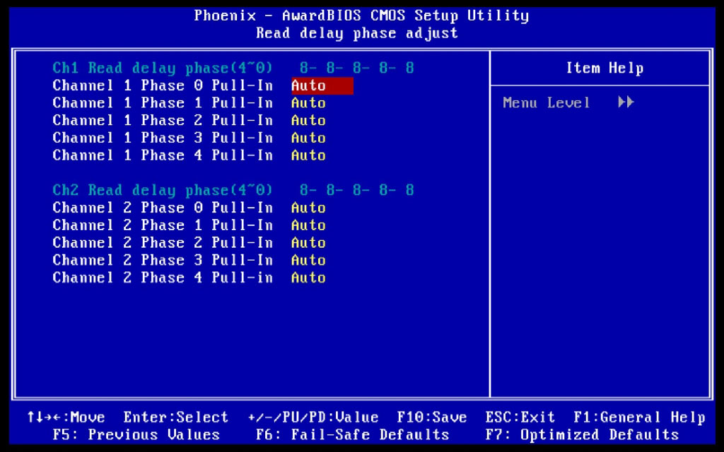 |
TRD Phase Adjust
This BIOS function is best explored by more advanced tweakers and benchmarkers; our own findings are as follows.
Options for this function are AUTO and ENABLED
Default for all phases is AUTO
AUTO: Unlike the DFI P35 T2R BIOS, setting AUTO will not disable the function of the tRD Phase shift registers; rather the BIOS attempts to apply any phase shifts it thinks are possible. While this works well for the most part, there are times when overclocking that increasing the Performance Level by 1 in the DRAM timing page and setting all the phases to Enabled may be the best course of action.
ENABLED: Sets the corresponding phase of the TRD cycle to -1. If we set a Performance Level of 7 in the DRAM page, using ENABLED for any of the phases will set the Performance Level of the selected Phase to 6, i.e. TRD -1 for the corresponding phase and channel.
Both channels have independent phase adjustments, and the maximum advantage of setting a phase to ENABLED occurs when the same phase from both channels is set to ENABLED simultaneously. Please note not all of the phases are active at all times. The number of active phases is dependent on the memory divider used i.e. the number of FSB cycles that are active in relation to the number of active memory bus cycles.
Still on our feet (BIOS)
Using AUTO for all sub-timings is generally acceptable until we start pushing for every last MHz of bandwidth and latency. The BIOS defaults are generally tight enough for reasonable performance on 24/7 PCs. We used Memset while running Windows XP to check where the AUTO DRAM timing defaults set the memory parameters. The timings shown by Memset were noted by us and entered manually into the relevant BIOS functions. We then began to tighten these values one at a time, noting the effects of any changes on bandwidth, latency, and stability. For benchmarking, we tend to use Memset once the XP operating system has loaded rather than entering overly tight settings directly in the BIOS. We can then begin to tighten the sub-timings far beyond 24/7 settings.
Additional Setting Ranges:
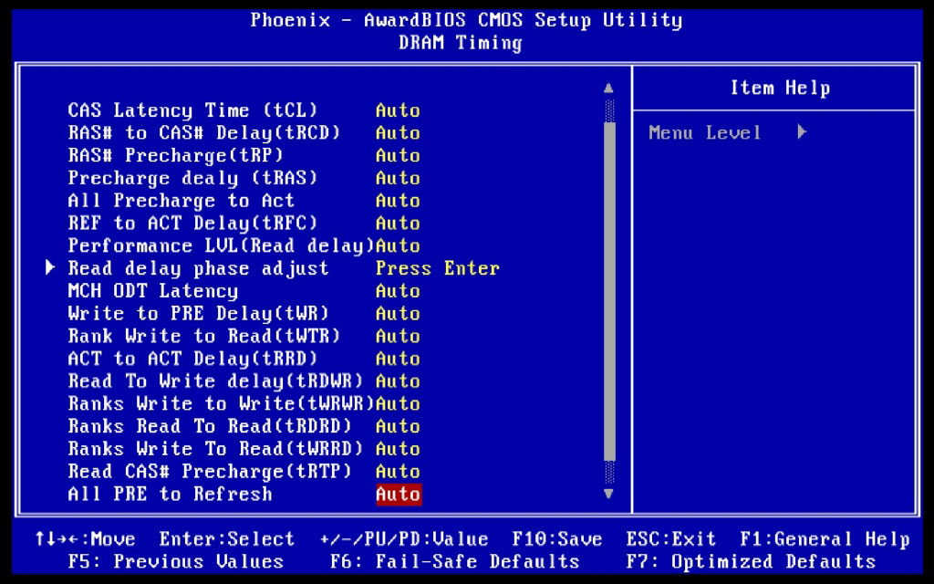
Ref to Act Delay (TRFC): The range of use for 1GB modules in 2GB setups is anywhere from 20-40 depending on overall memory speed. Lower values are more aggressive and give boosts in Read Bandwidth. For double density (2GB) modules, a higher tRFC range is required. For 4GB of memory running up to 1100 MHz, a value of 42 and above is usually required (54 is more compatible). For 8GB of memory a minimum value of 54 should be used.
MCH ODT Latency: ODT (On Die Termination) is used to match the MCH output impedance to the termination resistance of the RAM. Use of 1-2 is fine in most cases. Even for 4GB overclocking we did not find that more than a setting of 1 was required.
Write to PRE Delay (tWR): Range is from 10-13. For high RAM speed, use 12 and above for stability; for benchmarking 10-12 will be faster. Lower is faster.
Rank Write to Read (tWTR): Range is 9-11. Use 11 for stability and 10 or 9 for benchmarking. Lower is faster.
ACT to ACT Delay (tRRD): Range is 2-5. 3 is a good setting that allows high enough FSBs for most users. Higher numbers result in less memory read performance.
Read to Write Delay (tRDWR): Range is 8-9. 8 is ideal for most users; higher values are slower.
Ranks Write to Write (tWRWR): AUTO
Ranks Read to Read (tRDRD): AUTO
Ranks Write to Read (tWRRD): AUTO
The ranges for all these settings are quite well manipulated by SPD and BIOS. For those wishing to experiment, 4 is the lowest and most aggressive setting. 5-4-5 may work for SuperPi type benching. There is a slight write/copy speed increase with tighter settings, but this is only useful for extracting the last ounce of performance. For stability these are best left on AUTO
Read CAS# Precharge (tRTP): 2-3 works well on this board for most users. 2 is used for benchmarking while 3 and upwards are best for stability.
ALL PRE to Refresh: Range is 4-5. A setting of 4 is fine for most benchmarking, unless shooting high over 500FSB.
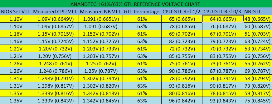
GTL - Not again!
CPU GTL reference voltage values are employed as threshold voltages by internal, on-die comparators used to determine whether each switch of an incoming data signal on either the FSB data or address busses is meant to represent a logic high or logic low (1 or 0). Adjusting these reference voltages in effect shifts the level in which the signal is seen as either high or low by the processor. As FSB is increased, the switching frequency is increased (by definition) meaning that each low to high or high to low voltage transition must occur at an accelerated rate.
This reduction in signaling margin, coupled with a more exaggerated ground bounce and overshoot, often requires manual adjustments in these thresholds if the system is to remain stable at the higher FSB speeds. Reducing or increasing the GTL reference voltages around a given percentage margin of the applied VTT by only a few millivolts can drastically affect processor stability. Imagine the processor detecting a 1 on a data transfer line when an incoming signal is in fact supposed to be low (0) - not surprising, the result is a BSOD, a complete system hang, or possibly even an undetected corruption of critical system data.
The added load capacitance of dual die processors (current Intel quad-core processors) usually requires more signaling drive as the FSB frequency is increased resulting in a need to raise VTT voltage. Any adjustment to VTT may also in turn require changes to GTL reference voltages in order to support proper data transfer margins. For 65nm processors the ratio of any GTL voltage to VTT is around 67% for both CPU and Northbridge (NB) GTL voltages; 45nm processors require that this percentage be closer to 61%-63%, again for both CPU and the NB. For example, for a VTT of 1.10V a 45nm processor would require a GTL reference voltage in the region of about 0.671V (61% of VTT) to 0.693V (63% of VTT).
DFI's approach to providing the user with ultra fine control of GTL reference voltages is unsurpassed in the motherboard industry, although working with an ultra fine scale such as this requires a significant dedication of time in order to get things right. In fact, some users enjoy this type of tweaking while others may feel it is akin to pulling teeth. In order to address this situation DFI has gone to the trouble of releasing a scale showing equivalent VTT/GTL percentages and associated BIOS settings.
We have found the scales themselves to be quite broad in range so we are providing a condensed version, taken from measurements using our own board here in the lab. The major issue here is that no two boards/CPUs are likely to behave in the exact same manner. This being the case, the small chart below is only intended to provide a starting point for any adjustments that may need to be made to your particular setup.
 |
Easy
500FSB E8500 Setup guide (easy starting point)
In order to make things as easy and presentable as possible we decided to provide users with a video setup guide showing how to run 500FSB with an Intel E8500 processor. We cannot guarantee the settings shown in the video will work on all systems as component choices will play a huge part in how far the board can clock. Secondly, GTL values vary from board to board and across processors adding further variables in to the mix. We attempted to keep the setup as simple as possible whilst enabling all key chipset registers for performance. If there is enough demand, we may venture into a quad-core overclocking guide too - although 400-420FSB is attainable with a minimum of BIOS level adjustments, so a guide is not really necessary.
Conclusion
DFI's execution of the P35 T2R motherboard was so close to perfection that any board released after it was bound to face an uphill task to live up to the performance, compatibility, and ease of use that has become synonymous with the product. The LANParty X48 T2R board has managed to equal the P35 when it comes to the simple things like USB ports and plug-in peripherals working as they should - we had no issues to speak of with any of our peripherals whilst using the board. However, overclocking the board to its limits is a little bittersweet.
It's sweet that the fine tuning options allow running components like memory at high bandwidth with the lowest VDIMM we have ever managed with our memory modules. The other positive is that users who don't want to go for elusive levels of FSB will find that the board will run fine without any need of tuning GTL levels right up to 485FSB for dual-core 45nm processors and 420FSB for quad-core 45nm processors. The bitter aspect is that boards from ASUS such as the Rampage Formula are in direct competition to DFI's offering in this segment and can run ultra high FSB speeds and lower tRD levels with relative ease.
As a result of this, there are times when performance on the ASUS boards is actually better than our achievements on the current DFI BIOS and with far less overall effort and time expenditure. Mind you, DFI still has an edge when it comes to flexibility for users who wish to run 8GB of memory. Access to all known chipset registers allows users to give and take on performance so that they can run high processor and memory speeds even with all the DIMM banks populated - there is no doubt DFI is the market leader for memory overclocking.
 |
Right at the very top-end of the performance ladder, we know DFI are working hard to pry everything they can from the X48 chipset, and in order to succeed they need to be able to provide that last few percent of headroom that people have come to expect from DFI products. Right now, for outright brute force overclocking, realizing that additional 1%-2% headroom is not possible. The board's current strengths may not be enough to win over the type of user that will generally choose this type of product to "race".
What we have here is a motherboard not quite able to dominate the DDR2 sector outright, but it certainly sets new standards in other regards. If tweaking is your thing and you have the patience to work with the extensive BIOS options, there is no doubt that the X48 T2R will keep you occupied for a long time. However, DFI's own P35 offers everything a user could need and can be teamed with a dual-GPU card to get around the P35 chipset limit of having a single x16 bandwidth PCIE slot.
We were hoping for a little more performance from this board and despite DFI's efforts thus far, we did not find the final few percent that would have given this board top-DDR2-dog status for 2GB and 4GB memory overclocking (that title still belongs to DFI's P35 LANParty board), but it's certainly an interesting contender. So interesting, that if you are not ready to move to DDR3 and want to run CrossFire, then we suggest you take a look at it.


