Original Link: https://www.anandtech.com/show/2354
DFI UT P35-T2R: Tweakers Rejoice!
by Rajinder Gill on October 18, 2007 2:00 PM EST- Posted in
- Motherboards
Overclocking with the DFI UT P35-T2R Motherboard
The last three months have seen the overclocking enthusiast sector bombarded with motherboards based around the Intel Bearlake (P35) chipset. While it has become an expectation for many to see boards from the main players up front and ready to go at product launch, early adopters have naturally expected DFI to be fashionably late to the ball with their own LANParty series offering. In terms of business, the enthusiast sector is an area of the retail market where being late does not earn the "money shot"; vital sales are lost in delays, no matter how good the product is - the delay is costly. So costly that many of the leading players in the once hot AMD S939 sector such as DFI, abit, MSI, Albatron, Chaintech, Shuttle, and EPoX have seen their market shares dwindle (sometimes drastically to the point of not being around anymore) since the introduction of the Core 2 Duo from Intel and the resulting market switch by the enthusiasts to the blue camp.
This time around DFI managed a reduced delay period of two months behind the official Intel Bearlake chipset rollout, greeted by applause from most tweakers who have been awaiting a killer product from the company since the "glorious" NF4 era. We thought the RD600 would fill that role last year, but it came up short in performance even though the BIOS options foretold the future about DFI's BIOS designs on Intel product. DFI managed to hit a home run with the Infinity 965-S Dark. Unfortunately, everyone had left the P965 ballpark to watch the P35 play in a new stadium by that time. Hopefully, their X38 product will be released in the coming weeks but until then (probably afterwards also based on early numbers), we think most people will be more than satisfied with the UT P35-T2R - provided you can afford it and do not have a need for multi-GPU benchmarking.
Beyond color enhancing UV lights to show off the board, the enthusiast knows that beauty in electronics, as with all other things, can often lie only skin deep. Rigorous in-house testing by DFI to iron out BIOS kinks was chosen over sending out boards at the chipset launch. This was done in an attempt to nail issues before users spent their hard earned dollars for partial functionality. As a matter of fact, anyone who buys motherboards close to official chipset launch dates should be fully versed in the ritual BIOS flashing regimen often required for long-term usefulness. Running a few quick benchmarks featuring high front side bus speeds might grab some early headlines, but it does not indicate a board's actual performance capability or stability. Put in perspective for the end-user, the two month delay is not such a bad thing, if a more solid and compatible motherboard is the end result.
Due to the very extensive BIOS options on this motherboard, assessing a product like this demands extra time. It also forces you to go over the options with greater detail while explaining their use and determining the worth of performance benefits when changing these options. While we are certainly not BIOS engineers, we are hoping that the time we have taken to go beyond the scope of normal motherboard review criteria will be welcomed by our readers, who are often just as confused as we are when we first take a look at a new DFI BIOS.
The goal then of this article is to take a focused look at how to properly set up and overclock this latest DFI offering, and even if you're not specifically planning on purchasing this motherboard we hope to provide some insight into what is involved in reaching top overclocks with Intel's impressive P35 chipset. In the near future, we will be able to provide direct overclocking performance comparisons and capabilities of this board against additional motherboards in the upper-end market sector. In the meantime, our results today are more of a dog and pony show as to what the board is capable of under various overclocking scenarios.
Additionally, we will be providing a catalog of "How to Guides" that will outline the BIOS settings utilized, BIOS option explanations, and recommended setups in our motherboard forum as we roll out these articles in the coming weeks. We welcome your input, suggestions, and ideas for improving this type of content. For now, let's take a look at DFI's latest board and its general performance results before we hit on the overclocking features.
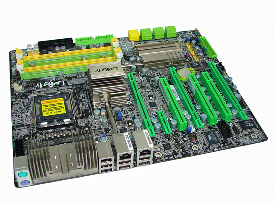
Board Features
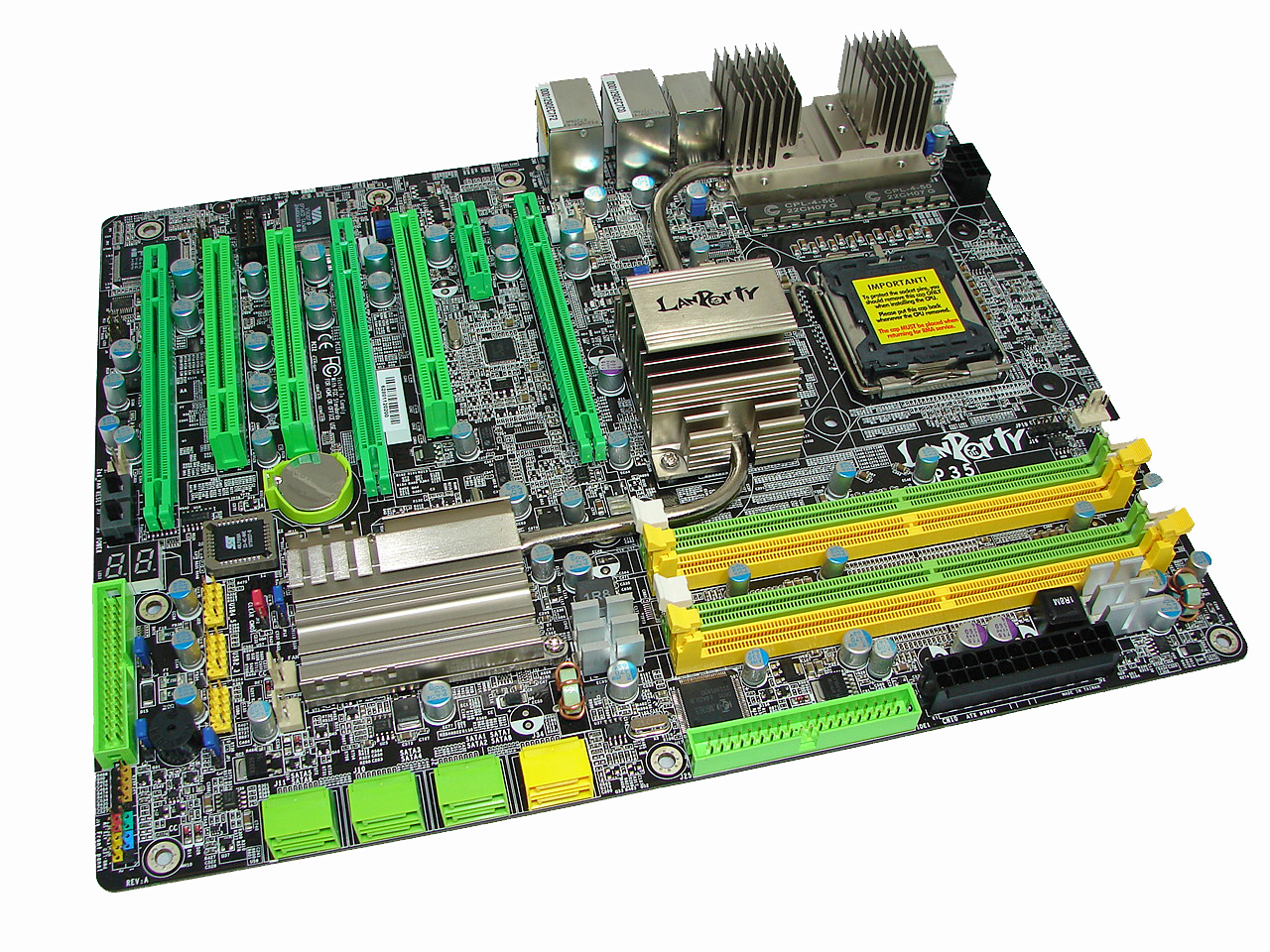 |
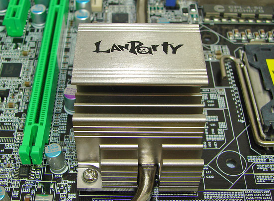
Our typical expectations were to see the standard orange or yellow LANParty color scheme, change is in the air and lime green is the flavor of the month. No matter the color scheme, the general layout of this board is nearly flawless.
 |
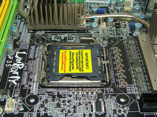
A clean CPU socket area ensures compatibility with large air-coolers. We do recommend that users consider having enough space for an additional fan to provide airflow over the PWM and Northbridge heatsink, if they intend to use more than 1.6V on the Northbridge. The 8-pin power connector sits at the top left corner of the board, close to the PWM circuitry, with enough room to allow the use of bulkier connectors without any interference from surrounding components.
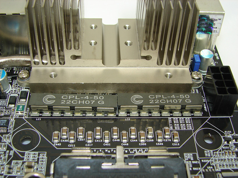
A more noteworthy subject is the 8-phase Digital PWM circuit, using the Volterra VT1115MF buck controller and associated fast-switching, high-bandwidth "Digital" MOSFETs. This solution has received mixed responses from overclockers, some feeling that Digital PWM does not have sufficient durability for an extreme overclocking motherboard. The current 8-phase design has managed to run overclocked quad-core CPUs completely Prime load stable at speeds of up to 4GHz. However, the jury is still out as to the effectiveness of the current Digital PWM design when quad-core CPUs are super-cooled. In the past, VCore settings over 1.6V and CPU speeds over 4GHz have not fared too well on lesser 6-phase implementations of DPWM, especially in high CPU load benchmarks.
DFI utilizes a heat pipe system that connects the PWM, P35, and ICH9R together to provide a cooling solution that works quite well, until you really push the board. At that point, additional cooling from active air or water solutions is required to properly cool these critical components. DFI engineered an extension joint (Transpiper) that attaches to the ICH9R heatsink to help carry heat within this system out of the chassis. There are numerous mounting configurations, with the most logical being to connect the highest heat producing area (the PWM heatsink) and have the Transpiper assembly exiting the PC case, so that heat is removed from the case, in theory reducing all internal component temperatures.
This system typically worked well with an air-cooling setup on the CPU and pushing the board to its limits on air. However, we did not notice any benefits during heavy overclocking sessions with water or cascade cooling. In fact, the hot air exiting the test case from our OCZ 1000W or 1200W power supplies seemed to have a reverse effect during extended overclocking sessions with the Transpiper located in front of the PSU fan as recommended by DFI. As such, DFI offers a version of this board without the Transpiper option for these users, or ones who want to save about $20.
That's not all; there is also a heat transfer plate that can connect from the CPU IHS to the PWM heatsink, sandwiched between the IHS and user CPU cooling solution. Our own thoughts are that users are best advised not to use this plate, as the temperature of both the PWM and CPU seem to suffer as a result. A closer look at the PWM heatsink mounting holes for this transfer plate shows that the width between the two holes is only a quarter of an inch offset from the mounting dimensions of the already available MIPS DFI 680i LT MOSFET waterblock (the key phrase here is "already available"). Had the holes on the PWM heatsink aligned with the MIPS 680i LT block without requiring a redesign ,or the removal of DFI's own PWM heatsink for functionality, current owners of the block and perspective water-cooling users could have been saved some time and perhaps money.
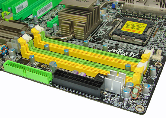
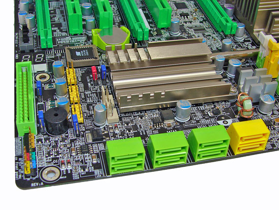
DFI once again adhered to their typically overclocking friendly layout, easily accessible CMOS battery, onboard power and reset switches featuring EZ CMOS clear, and of course the LED POST Code display. The floppy drive connector sits at the lower edge of the board to the right of the POST Code display. The six Intel ICH9R SATA ports are located at the lower right edge of the board, facing to the right making connector insertion a little awkward at times once the board is mounted in a case. There are also two JMicron JMB363 SATA ports situated above the Intel SATA ports.
The memory slot connectors are situated almost in line with the primary PCI Express connector; large graphics cards such as the 8800 GTX may have to be removed when swapping out memory modules. The 24-pin ATX connector is placed to the right of the slots and does not hinder the use of the IDE connector below it. There are six onboard fan headers, all logically placed in high heat production areas, with both BIOS and OS Smart Guardian fan control options.
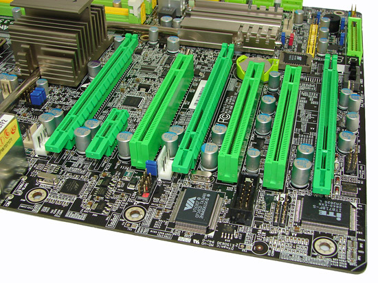
The expansion slot layout is comprised of three PCI Express x16 slots (one x16, one x4, and one x1 slot), one PCI Express x1 slot, and three PCI slots. The supplied Bernstein Audio module features the Realtek ALC885 8-channel High Definition Audio CODEC and has its dedicated connector placed between the PCI slots, rendering one of the PCI slots inactive if the module is used. There are three onboard USB connectors for an additional six USB ports, a connector for an external COM port, one IrDA connector, one CIR connector, and a connector for the second IEEE-1394 port.
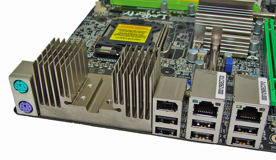
The rear I/O options include six USB ports, an IEEE-1394 port, two Gigabit LAN ports with teaming options, and finally the standard PS/2 keyboard and mouse ports.
Test Setup
| DFI UT P35-T2R Standard Benchmark Testbed |
|
| Processor | Intel Core 2 Quad Q6600 Quad Core, 2.4GHz, 8MB Unified Cache, 9x Multiplier, 1066FSB |
| CPU Voltage | 1.2500V |
| Cooling | Tuniq Tower 120 |
| Power Supply | OCZ ProXStream 1000W |
| Memory | OCZ Flex PC2-9600 (4x1GB) |
| Memory Settings | 4-4-4-12 (DDR2-1066) |
| Video Cards | MSI 8800GTX |
| Video Drivers | NVIDIA 163.71 |
| Hard Drive | Western Digital 7200RPM 750GB SATA 3/Gbps 16MB Buffer |
| Optical Drives | Plextor PX-B900A, Toshiba SD-H802A |
| Case | CoolerMaster Stacker 830 Evo, Lin Li PC75 |
| BIOS | DFI 9/13 |
| Operating System | Windows Vista Ultimate 64-bit |
| . | |
With such a vast array of overclocking BIOS functions at our disposal, a decision was made to stick with a single operating system environment. Microsoft XP SP2 was chosen due to its maturity, taking away some of the time burden looking for possible software level conflicts that may exist on a newer OS (though we ventured to our standard Vista test suite for the non-overclocking benchmarks). This does not mean to say that the board cannot work with Vista at present when overclocking. We are just trying to eliminate possible downtime on non motherboard/BIOS related issues and also considered the fact that a vast majority of overclocking enthusiasts have not switched to Vista (yet).
The test setup utilized the supplied Transpiper, set up to exit our Lian Li PC75 case via the space available by not inserting the supplied I/O backplate. The fin section of the Transpiper heatsink was aligned with the exhaust fan of the OCZ 1000w ProXStream PSU, though at times we felt this might not have been the best solution during extended overclocking sessions because of the already high temperature of the PSU exhaust. Another reason this setup may not be ideal when benchmarking is that the Transpiper solution is partially handicapped by an adjustable construction. We found most of the heat that was transferred into the single heatpipe never quite made it past the elbow joint connecting to the dual pipe heatsink. The biggest gain in temperature reduction was realized by simply pointing a fan at the PWM heatsink itself.
We could not find any gains in using the supplied CPU to PWM heat transfer plate; CPU temps with the plate installed were considerably higher at full load (~10C). This was partially due to the increased thermal resistance of an extra surface, which decreases thermal transfer potential from the most critical junction of a cooling solution - directly over the CPU die. We also need to consider the concave or bi-concave bases of some modern coolers and waterblocks and indeed the IHS itself (unlapped). The heat transfer plate would need to be quite flexible to ensure good contact when under pressure.
We used our QX6800 G0 ES CPU, concentrating on the 8x and 9x multipliers that both our air- and water-cooled setups can take advantage of currently. The CPU itself is a particularly high temperature sample of a G0 stepping; load temps were around 15C higher at equivalent voltages in comparison to some of the better Q6600 G0 examples we have in the labs. We later lapped the IHS flat (as flat as possible) which resulted in a seven degree drop in load temperatures, but that still ends up around 8C higher than our best Q6600 temperature ranges.
Both high resolution 1920x1200 and 1280x1024 resolution game benchmark tests were run to find performance benefits for gamers, should such advancements through BIOS tweaking exist. We utilize new drive images on each board in order to minimize any potential driver conflicts. Our 3DMark results are generated utilizing the standard benchmark resolution for each program. We run each benchmark five times, throw out the two low and high scores, and report the remaining score.
We limited our standard Vista test suite to a few benchmark results to indicate the general performance of this board. After all, a P35 is a P35 for the most part at stock settings, with most P35 boards scoring within 1%~2% of each other. It really does not matter if you utilize a $90 abit or Gigabyte P35 board or the $200+ versions from ASUS or DFI as stock performance will not vary much in most cases.
As such, we decided to take a different look at this board and focus on overclocking. This board was designed for the PC Autobahn and not your typical school zone road or office park avenue. Our overclocking tests will only show results on this board for now, but we will expand coverage to include direct comparisons as we review other boards that are designed for the overclocking enthusiast market sector.
Synthetic Graphics Performance
The 3DMark series of benchmarks developed and provided by Futuremark are among the most widely used tools for benchmark reporting and comparisons. Although the benchmarks are very useful for providing apples-to-apples comparisons across a broad array of GPU and CPU configurations, they are not a substitute for actual application and gaming benchmarks. In this sense we consider the 3DMark benchmarks to be purely synthetic in nature but still valuable for providing consistent measurements of performance.
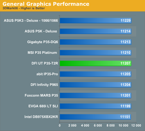
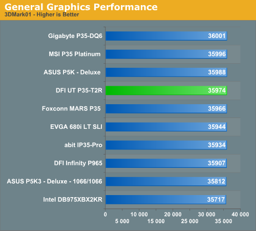
In our 3DMark06 test, the P35 boards are basically even in this test. The DFI board did not exhibit any issues during repeated testing in this CPU/GPU intensive test. In the more memory and CPU throughput sensitive 3DMark01 benchmark we see our DFI board performing well though it's just slightly off the top mark. We typically see this in the DFI boards that are tuned more for overclocking results than stock performance. The differences in performance are not really noticeable in either 3DMark unless you're looking to reach the top of the ORB. That of course requires some serious overclocking as well, and we have a good feeling the DFI was designed to do exactly that with the right setup.
General System Performance
The PCMark05 benchmark developed and provided by Futuremark was designed for determining overall system performance for the typical home computing user. This tool provides both system and component level benchmarking results utilizing subsets of real world applications or programs. This benchmark is useful for providing comparative results across a broad array of Graphics, CPU, Hard Disk, and Memory configurations along with multithreading results. In this sense we consider the PCMark benchmark to be both synthetic and real world in nature, and it again provides for consistency in our benchmark results.
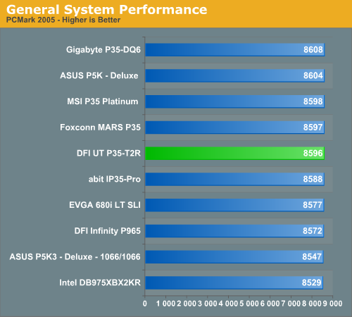
Our PCMark05 scores mimic the results from our 3DMark benchmarks with differences between the boards not exceeding 2%. While this benchmark is designed around actual application usage, we will see if these results mirror our application testing.
Media Performance
We will take a brief look at general media performance with our test suite that includes Adobe Photoshop CS2 and Adobe Photoshop Elements 5.0.
We utilize the PC WorldBench 6.0 Test for measuring platform performance in Adobe's Photoshop CS2. The benchmark applies an extensive number of filters to the test image and heavily stresses the CPU and storage systems. The scores reported include the full conversion process and are represented in seconds, with lower numbers indicating better performance.
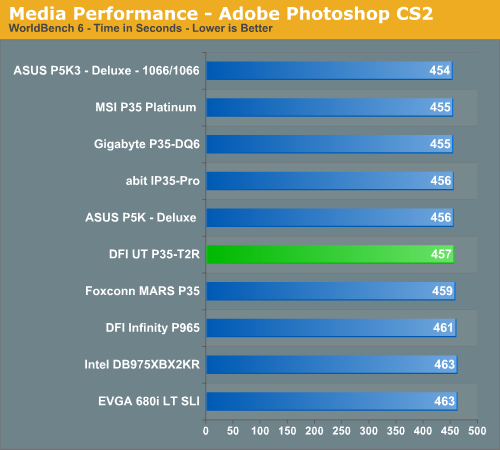
This test requires a balance between CPU speed and a fast storage sub-system. Once again the P35 boards are bunched together with only four seconds separating them. The DFI board falls into the middle pack of the P35 boards although its performance is more than acceptable.
Our next test is one recommended by Intel, but the test itself appears to be fair and results are very repeatable. This test simply measures the amount of time required to fix and optimize 103 different photos weighing in at 63MB. Time is measured in seconds, with lower times resulting in better performance
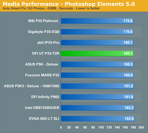
This test heavily stresses the CPU subsystem and as we can see, the P35 boards all perform nearly identically with the DFI board in the top grouping.
Media Encoding Performance
We are utilizing Nero Recode 2 for our video encoding test. The scores reported include the full encoding process and are represented in seconds, with lower numbers indicating better performance. For this test, we take our original Office Space DVD and use AnyDVD to rip the full DVD to the hard drive without compression, thus providing an almost exact duplicate of the DVD. We then fire up Nero Recode 2, select our Office Space copy on the hard drive, and perform a shrink operation to allow the entire movie along with extras to fit on a single 4.5GB DVD disc. We leave all options on their defaults except we uncheck the advanced analysis option.
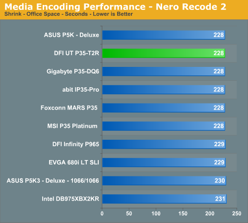
Again, in this CPU and disk intensive test the P35 boards all score nearly identically - not surprising considering the boards utilize the same chipsets. The DFI board scores at the top of the grouping this time.
Audio Encoding Performance
We will utilize iTunes 7.4 for our audio encoding tests as it is one of the most utilized audio applications available due to the immense popularity of the iPod. As in previous articles, we are using an INXS Greatest Hits CD for testing, which contains 16 tracks totaling 606MB of songs. We use iTunes to convert our WAV files into an ACC compatible format. We utilize the 256kbps and variable bit rate option.
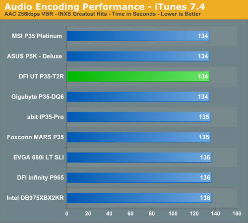
We usually see iTunes favoring systems with excellent CPU throughput and these tests indicate the DFI board is up to speed in this area.
File Compression Performance
Another CPU crunching utility is WinRAR 3.70, which provides for computationally intensive file compression. Our test folder contains 444 files, ten subfolders, and 602MB worth of data. All default settings are utilized in WinRAR and our hard drive is defragmented before each test.
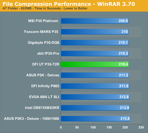
Yet again, the DFI UT P35-T2R is performing well in a test that stresses overall memory latencies and CPU/Memory throughput. The nature of file compression is such that memory is accessed almost constantly in a very random fashion, so page misses requiring additional time as memory banks are swapped is common.
Gaming Performance
As usual, gaming performance was tested with a variety of current games. We ran our benchmarks at a 1280x1024 resolution with high quality settings
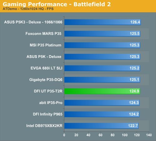
Battlefield 2
This benchmark is performed using DICE's built-in demo playback functionality with additional capture capabilities designed in house. During the benchmark, the camera switches between players and vehicles in order to capture the most action possible. There is a significant amount of smoke, explosions, and vehicle usage as this a very GPU intensive Battlefield 2 benchmark. We run Battlefield 2 using medium quality graphics settings available in the video settings. The game itself is best experienced with average in-game frame rates of 35 and up.
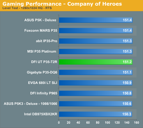
Company of Heroes
Company of Heroes was released last year but is still one of the high points of the RTS genre. The game is extremely GPU intensive but can also requires a fast CPU at times. The game contains a built-in performance test that utilizes the game engine to generate several different action scenes. We find the performance test gives a good indication of how well your system will perform throughout the game. Some of the in-game action sequences can be more demanding than the performance test, however, so we find the game to be enjoyable with an average frame rate score in the performance test above 35FPS.
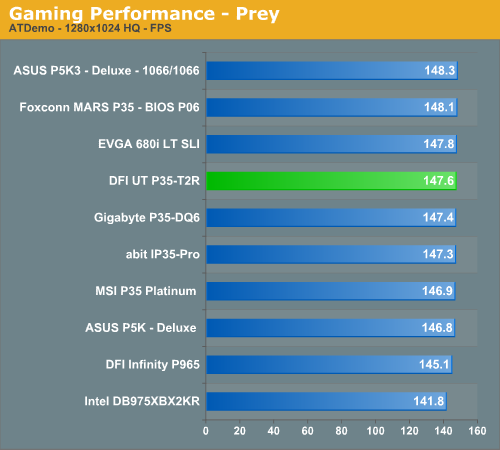
Prey
Prey offers some superb action sequences, unique weapons and characters, and is a visually stunning game at times. It still requires a very good GPU to run it with all of the eye candy turned on. We set all graphic settings to their maximum except for AA/AF and utilize a custom timedemo that takes place during one of the more action oriented sequences. We generally find the game to be enjoyable with an average frame rate above 35FPS.
Gaming Summary
Although the DFI board did not finish first in our benchmarks, it did perform very consistently with differences only averaging around 1% between the P35 boards. This only reiterates our original statements about the performance of the P35 chipset: just about any board based on it will perform great and performance differences between boards is generally less than 2% at stock speeds.
We did not need to test the DFI board to figure this out, but wanted to provide the preceding results in the interest of completeness. Now let's release the hounds and see what this board is really capable of doing; in other words, let's delve into the BIOS and take a look at how to overclock this board.
Gearing up for Overclocking
Before we continue further, users are encouraged to check that standard BIOS settings with stock (AUTO) parameters for all overclocking functions are working as they should be. This primarily includes eliminating default DRAM setting issues, and/or OS driver level conflicts. The following software is of use for these tasks: Prime95, OCCT, MemTest, Dual Super PI 32M, Folding@Home, and the Futuremark 3DMark applications.
In terms of CPU stress testing software, always search for the latest version of software and make sure that the test itself does not have known bugs on newer hardware or software - there is always the possibility of incompatibility! A few hours of basic groundwork can save countless hours of uncertainty later on when the system is overclocked and random failures are experienced. Hardware selection can be crucial to ensuring success; again basic research can often eliminate poor component choices.
Important Performance Related BIOS Options (9/13 BIOS)
Please note that we have decided to work on explanations of BIOS settings we deem worthy of user adjustment when overclocking. Settings we have left out were found to function adequately at the default or AUTO setting.
Genie BIOS Setting
Boot Up Clock: Sets a safe user selected FSB speed for the system to revert to when an overzealous overclock fails.
PCIE Clock: Overclocking the PCIE bus can be useful for benchmarking, bringing small gains to overall scores. Unfortunately the P35/ICH9R combo does not have the potential for overall MHz we find with NVIDIA's 680i chipset which could run PCIE frequencies in excess of 150MHz for benchmarking. We also found that overclocking the PCIE bus frequency within the limits of the board exhibited a peculiar issue: the BIOS would revert the bus to x1 PCIE mode for the graphics card between reboots. We managed to get around this by loading optimized defaults every time it occurred and then reloading the overclocked profile we were working on, from a saved CMOS bank. Using the Intel SATA ports, expect around 115MHz to be the maximum. Those wishing to explore PCIE frequencies in excess of 115MHz for benchmarking are advised to use the JMicron controller; we have seen examples of up to 125MHz using this method.
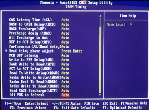
DRAM Speed
Available options are for this function can be seen in the following images:
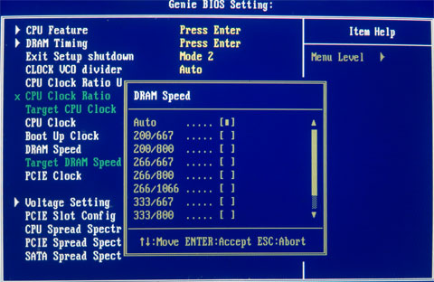
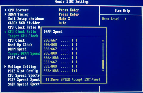
We will concentrate on the following 266/667 and 333/800 strap/dividers. The 266/667 represents a 1066FSB chipset strap with 4:5 memory ratio and the 333/800 represents a 1333FSB chipset strap with a 5:6 memory ratio.
Why Choose the 266/667 and 333/800 Ratios?
Both of these Northbridge strap/divider combinations offer the best balance between performance level and FSB capabilities within sensible voltage ranges. We are interested in five key attributes to provide an intelligent overclock for all-around performance in games and workstation software, these are:
- Raw CPU MHz per volt
- Memory bandwidth
- Memory/chipset latency
- Memory copy speeds
- Memory write speeds
Herein lies the potential advantage of the P35 chipset. Having been designed from the ground up with quad-core CPUs in mind, we have at our mercy increased FSB and performance level margins over previous chipsets. It is mandatory to explore these advantages in order to satisfy the justification of an "upgrade" from older hardware.
This brings us to the 266/667 strap. We found this strap allowed for 2GB RAM overclocks between 450/475FSB. The maximum the board will hold absolutely stable for most users is around 475FSB with the 266/667 or 1333/800 NB setting (with judicious GTL tuning if one is not to succumb to a brute force approach of using excessive voltages without tuning the BIOS with finesse), using a performance level (read delay) of 6 for 266 or 7 for 333.
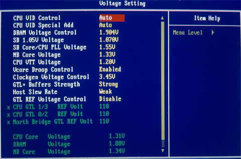
CPU VID Control: This function sets the current CPU Vcore (range from 0.8v to 1.6v), this function can be used in conjunction with "CPU VID Special Add", for overvolting past 1.6v if required.
CPU VIDD Special Add: Used in conjuction with "CPU VID Control", sets a percentage of VCore over the applied voltage using the "CPU VID Control" function, maximum is 125% over 1.6V.
VCore Droop Control: Set this function to DISABLED for overclocking; counter-intuitively, the ENABLED setting causes the CPU core voltage to sag when the CPU is placed under load.
Taking a Look at the BIOS, continued
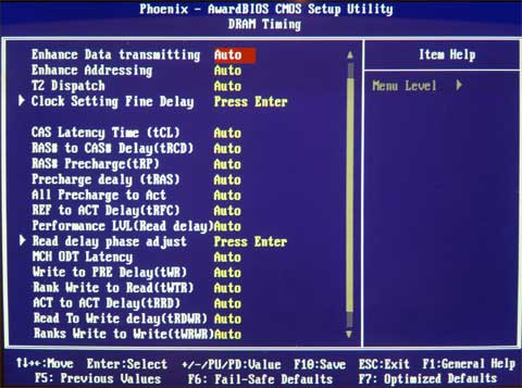
Regardless of individual memory timing preferences, to obtain best RAM/chipset latency performance we recommend that the following BIOS functions are set as follows for Micron D9 based RAM modules.
Enhance Data transmitting: FAST
FAST MODE: Gives latency and bandwidth improvements over the "Normal" setting without overly affecting memory stability or FSB overclocking potential throughout the frequency ranges of interest for everyday use.
TURBO MODE: Is more suited to benchmarking runs. This is a very aggressive setting, further improving latencies past "Fast" mode. Using "Turbo" mode may require that the "CH1CH2 Common CLK Crossing Setting" is set to "Nominal" rather than "More Aggressive". VNB requirements are 1.7V and upwards, hence this should be used strictly for short-term benchmarking.
Enhance Addressing: FAST
This brings additional gains of latency and bandwidth used in combination with the above settings for best overall system performance. Again the stability/voltage requirement hit is only minor for normal PC use.
The difference of using FAST for these two settings together, over NORMAL mode, can be seen clearly in the following synthetic Everest Cache and Memory benchmark screenshots:
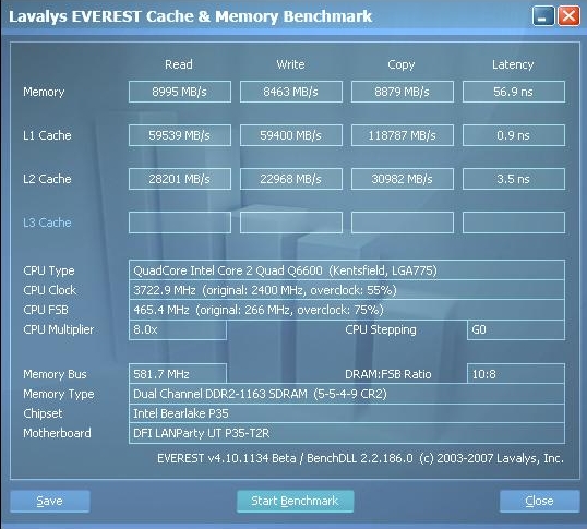
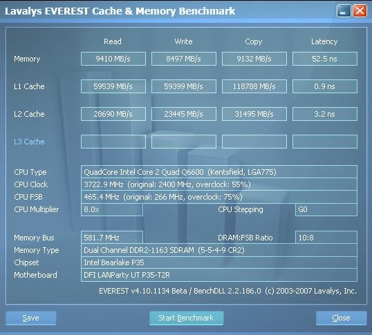
Although the BIOS defaults to Normal mode for both settings, there is no reason to veer away from setting FAST for both functions, provided you're using reasonable memory.
T2 Dispatch: Set this to Disabled, as it gives more overall stability when memory is clocked to high speeds.
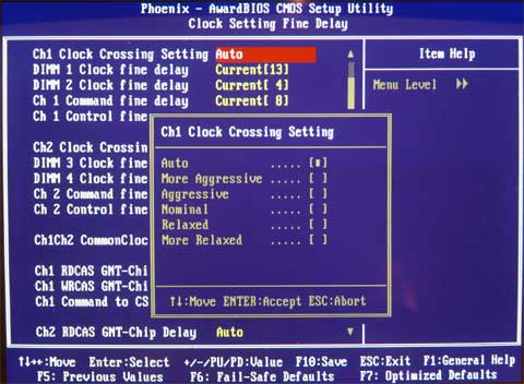
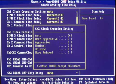
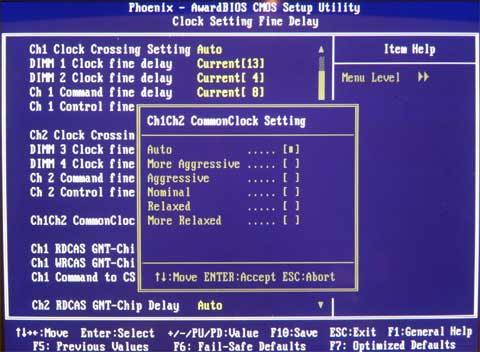
Channel 1 CLK Crossing Setting: More Aggressive
Channel 2 CLK Crossing Setting: More Aggressive
CH1CH2 Common CLK Crossing Setting: More Aggressive
24/7 systems using Micron D9GMH based modules will certainly want to take advantage of using all three of these settings in unison for a latency and bandwidth boost. We have found these three functions set to "More Aggressive" do not hinder the boards FSB progress up to 470FSB for absolute stability. Other RAM modules may not fare as well, unfortunately.
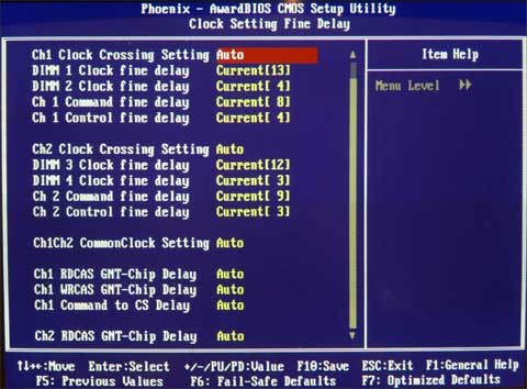
Clock Fine delays: For Both Channels, the 913 BIOS senses and adjusts these values automatically when set to CURRENT mode. DFI has notified users that manual setting ranges should not exceed a margin of three digits either side of the CURRENT setting auto sense. There is some variance at higher FSB levels (over 465FSB on quad-cores). The settings correspond to the DRAM slots in use (the slots filled with RAM are the point of interest). It is worth noting stable ranges on paper and checking back when raising FSB levels to see how the CURRENT setting reacts to FSB changes. If instability is experienced at random between reboots, it may be worth reverting to earlier ranges by setting the scales manually from your notes.
Even More BIOS Settings
PERFORMANCE LEVEL
Leaving this function set to Auto works very well within the FSB limits of the board for normal everyday use. For maximum performance and benchmark runs, we took a look at possible manual setting ranges.
Performance Level settings with the 266/667 strap/divider-
Level 5 is usable up to ~ 410FSB
Level 6 up to 475FSB using 2GB of RAM with quad-core CPUs
Performance Level settings with the 333/800 strap/divider-
Use level 7, this is good up to ~ 495FSB with the quad-core CPUs. Dual-core CPUs can use this strap/divider combination for benchmarking in excess of 500FSB if the CPU is capable of these FSB rates.
TRD PHASE ADJUST-
This BIOS function is best explored by more advanced tweakers and benchmarkers; our own findings are as follows.
Options for this function are between AUTO and ENABLED
Default for all phases is AUTO (this sets the current PERFORMANCE LEVEL in the DRAM page).
AUTO is best used for all phases when using the 266 chipset strap and associated dividers. The 266 strap is generally quite aggressive and does not allow lowering of Performance Level phases. Users can safely stay at AUTO without sacrificing large amounts of performance. For crazy tweakers, read on...
There are five phases of the Performance Level (TRD) cycle per channel;
'ENABLED': Sets the corresponding phase of the TRD cycle to -1. If we set a Performance Level of 7 in the DRAM page, using ENABLED for any of the phases will set the Performance Level of the selected Phase to 6, i.e. TRD -1 for the corresponding phase and channel.
Both channels have independent phase adjustments, and the maximum advantage of setting a phase to ENABLED occurs when the same phase from both channels is set to ENABLED simultaneously. (Check the 333/800 BIOS profile for a possible usage combination).
Using the 1333 strap has an immediate impact upon memory latency, which can be overcome in part by using a higher FSB level on a lower multiplier for an equivalent CPU MHz speed (assuming we stick to using the same strap). By manipulating combinations of the TRD phases together for both channels it is possible to reclaim some of the memory latency and bandwidth loss without the need for a large increase of FSB. The lowering of TRD phases is especially useful for 4GB overclocking with the 333/800 strap/divider and benchmarking at high FSBs with dual-core CPUs, again using the 333 strap.
BIOS TRD Phase Adjust
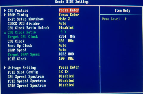
465FSB BIOS Settings
For our 465 FSB Prime stable test, we used the 333/800 strap. We set Performance Level 7, targeted a 465FSB x 8 CPU speed, and ran 4GB of OCZ Flex 9200. The remaining BIOS DRAM Settings were as follows:
| 465FSB BIOS Settings | |
| CPU Feature | |
| Thermal Management Control | Disabled |
| PPM (EIST) Mode | Disabled |
| Limit CPUID MaxVal | Disabled |
| CIE Function | Disabled |
| Execute Disable Bit | Enabled |
| Virtualization Technology | Enabled |
| Core Multi-Processing | Enabled |
| Exist Setup Shutdown | Mode 2 |
| CLOCK VC0 divider | AUTO |
| CPU Clock Ratio | 8x |
| Target CPU Clock | 3722MHz |
| CPU Clock | 465FSB |
| Boot Up Clock | AUTO |
| DRAM Speed | 333MHz/800MHz |
| Target DRAM Speed | DDR2-1116MHz |
| PCIE Clock | 100MHz |
| Voltage Settings | |
| CPU VID Control | 1.4375 |
| CPU VID Special Add | AUTO |
| DRAM Voltage Control | 2.12 |
| SB 1.05V Voltage | 1.07v |
| SB Core/CPU PLL Voltage | 1.55v |
| NB Core Voltage | 1.65 |
| CPU VTT Voltage | 1.60v |
| VCore Droop Control | Disabled |
| Clockgen Voltage Control | 3.45v |
| GTL+ Buffers Strength | Strong |
| Host Slew Rate | Weak |
| GTL REF Voltage Control | Enabled |
| x CPU GTL1/3 REF Volt | 115 |
| x CPU GTL 0/2 REF Volt | 115 |
| x North Bridge GTL REF Volt | 117 |
| DRAM Timing | |
| Enhance Data transmitting | FAST |
| Enhance Addressing | FAST |
| T2 Dispatch | Disabled |
| Channel 1 CLK Crossing Setting | More Aggressive |
| Channel 2 CLK Crossing Setting | More Aggressive |
| CH1CH2 Common CLK Crossing Setting | More Aggressive |
| CAS Latency Time (tCL) | 5 |
| RAS# to CAS# Delay (tRCD) | 5 |
| RAS# Precharge (tRP) | 4 |
| Precharge Delay (tRAS) | 9 |
| All Precharge to Act | 4 |
| REF to ACT Delay (tRFC) | 30 |
| Performance Level | 7 |
| Read delay phase adjust | SEE BELOW |
| MCH ODT Latency | 1 |
| Write to PRE Delay (tWR) | 12 |
| Rank Write to Read (tWTR) | 10 |
| ACT to ACT Delay (tRRD) | 3 |
| Read to Write Delay (tRDWR) | 8 |
| Ranks Write to Write (tWRWR) | AUTO |
| Ranks Read to Read (tRDRD) | AUTO |
| Ranks Write to Read (tWRRD) | AUTO |
| Read CAS# Precharge (tRTP) | 3 |
| ALL PRE to Refresh | 4 |
| PCIE Slot Config | 1X 1X |
| CPU Spread Spectrum | Disabled |
| PCIE Spread Spectrum | Disabled |
| SATA Spread Spectrum | Disabled |
| TRD Phase adjust settings | |
| Channel 1 Phase 0 Pull-In | ENABLED (TRD 6) |
| Channel 1 Phase 1 Pull-In | ENABLED (TRD 6) |
| Channel 1 Phase 2 Pull-In | ENABLED (TRD 6) |
| Channel 1 Phase 3 Pull-In | ENABLED (TRD 6) |
| Channel 1 Phase 4 Pull-In | ENABLED (TRD 6) |
| Channel 2 Phase 0 Pull-In | ENABLED (TRD 6) |
| Channel 2 Phase 1 Pull-In | AUTO (TRD 7) |
| Channel 2 Phase 2 Pull-In | ENABLED (TRD 6) |
| Channel 2 Phase 3 Pull-In | ENABLED (TRD 6) |
| Channel 2 Phase 4 Pull-In | ENABLED (TRD 6) |
Even though we have set Performance Level 7 in the DRAM page, this particular TRD Phase sequence is virtually running a Performance Level of 6 throughout the entire TRD cycle with the exception of a single TRD phase set to 7 (Channel 2 Phase 1) to create the breathing space necessary for the Northbridge to hold steady at 465FSB with 4GB of RAM. When setting a series of phases to ENABLED on both channels, Channel 2 will require an offset as can be seen in the list of settings we used above. If Channel 1 Phase 0, Phase 1 and Channel 2 Phase 0 are set to ENABLED, Channel 2 Phase 1 must be set to AUTO.
Running two or more corresponding phases at ENABLED on both channels is more aggressive, as it sets the corresponding TRD phase registers to -1 at the same point of the TRD cycle, resulting in a lower latency and thus a higher load on the chipset. The general advantage of TRD phase adjustments is to increase FSB margins while retaining significant amounts of latency and bandwidth at FSBs that fall between the borders of two Performance Levels.
Setting a single channel's phase to ENABLED while the corresponding phase for the other channel is set to AUTO results in a very slight gain in latency and bandwidth, which can be useful for maximizing overall performance.
The above timing and phase combinations are only applicable for the setting of 465FSB using the 333/800 divider and Performance Level 7. Scaling the FSB higher will require further tuning and perhaps returning some of the phases back to AUTO. We must consider that various memory settings can affect the level of TRD adjustments that can be made. Experimentation will be required by the user when changing CPU/RAM MHz (FSB) and also primary/secondary RAM timings.
All Other Sub-Timings-
Using AUTO for all sub-timings is generally acceptable until we start pushing for every last MHz of bandwidth and latency. The BIOS defaults are generally tight enough for very good performance on 24/7 PCs. The BIOS profiles we are including in this article have been tuned for maximum performance while retaining full system stability. We used Memset 3.3 while running Microsoft XP to check where the AUTO DRAM timing defaults set the memory parameters. The timings shown by Memset were noted by us and entered manually into the relevant BIOS functions. We then began to tighten these values one at a time, noting the effects of any changes on bandwidth, latency, and stability.
For benchmarking we tend to use Memset once the XP operating system has loaded rather than entering overly tight settings directly in the BIOS. We can then begin to tighten the sub-timings far beyond 24/7 settings. We have attached Memset screenshots for both our 24/7 stable and sub-zero benchmarking so that users can see how far we were able to push for maximum scores.
Additional Setting Ranges:
MCH ODT Latency: ODT (On Die Termination) is used to match the MCH output impedance to the termination resistance of the RAM. Use of 1-2 is fine in most cases. Even for 4GB overclocking we did not find that more than a setting of 1 was required.
Write to PRE Delay (tWR): Range is from 10-13. For high RAM speed, use 12 and above for stability; for benchmarking 10-12 will be faster. Lower is faster.
Rank Write to Read (tWTR): Range is 9-11. Use 11 for stability and 10 or 9 for benchmarking. Lower is faster.
ACT to ACT Delay (tRRD): Range is 2-5. 3 is a good setting that allows high enough FSBs for most users. Higher numbers result in less memory read performance.
Read to Write Delay (tRDWR): Range is 8-9. 8 is ideal for most users; higher values are slower.
Ranks Write to Write (tWRWR): AUTO
Ranks Read to Read (tRDRD): AUTO
Ranks Write to Read (tWRRD): AUTO
The ranges for all these settings are quite well manipulated by SPD and BIOS. For those wishing to experiment, 4 is the lowest and most aggressive setting. 5-4-5 may work for SuperPi type benching. There is a slight write/copy speed increase with tighter settings, but this is only useful for the extracting the last ounce of performance. For stability these are best left on AUTO
Read CAS# Precharge (tRTP): 2-3 works well on this board for most users. 2 is used for benchmarking while 3 and upwards are best for stability.
ALL PRE to Refresh: Range is 4-5. 4 works fine with quad-core CPUs all the way to 475 FSB. A setting of 4 is fine for most benchmarking, unless shooting high over 500FSB.
Quad-Core Overclocking
DFI P35 T2R VTT/GTL Tables
Fig 1. VTT Voltage and 67% GTL settings
 |
GTL scale for VTT 1.2v
GTL scale for VTT 1.3v
GTL scale for VTT 1.4v
GTL scale for VTT 1.5v
GTL scale for VTT 1.6v
VTT/GTL settings tables, see next page for setup info...
Quad-Core Overclocking, continued
Approximate VTT values and FSB ranges
VTT = 1.2V - 1.3V = Up to 400 FSB
VTT= 1.4V - 1.55V = 420-440FSB
VTT=1.6V (~1.58 actual) = 440-475FSB
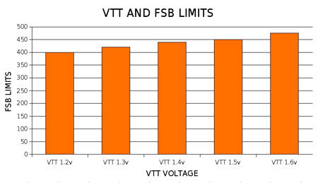
A few notes on applying values from the VTT/GTL table
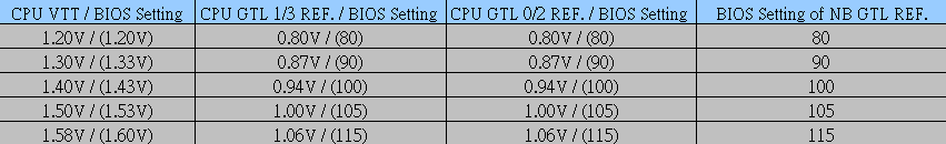
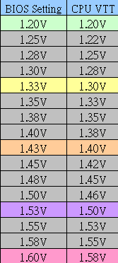
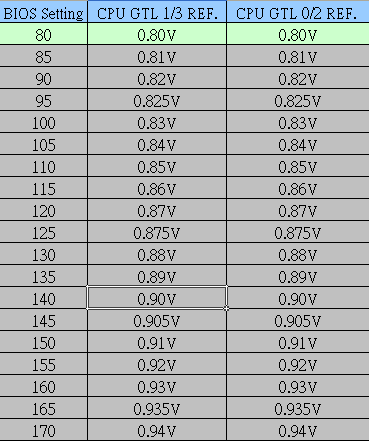
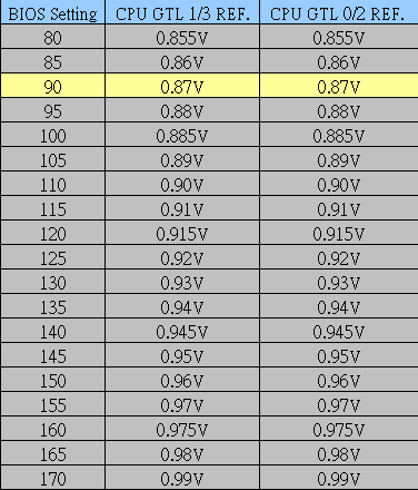
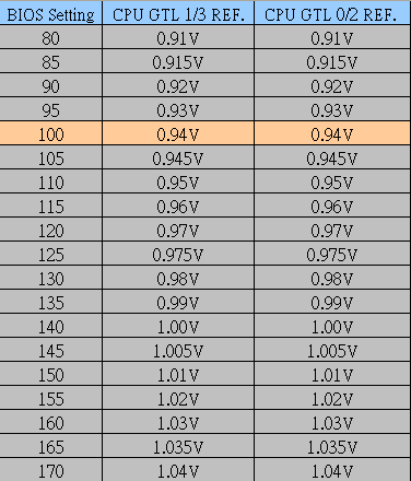
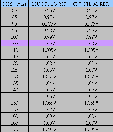
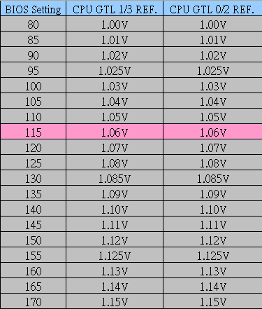
1) Fig 1. The first column shows BIOS and actual measured voltages for VTT (first value is measured VTT), the value in brackets is the voltage that must be applied in the BIOS to obtain the measured value. As can be seen, there is a small offset between the BIOS setting of VTT and the actual DMM measured onboard voltage. An average representative figure has been used for the tables. We have found a general variance on boards either 0.1V above or below these figures. Each motherboard will have different sweet spots for GTL values due to this small offset.
2) GTLs set to 66%-70% of VTT seem to be at the most effective point for "stable overclocking" of quad-core CPUs. The highlighted color bar in each VTT/GTL table shows the approximate 67% point of VTT and the corresponding numerical value that needs to be set in the BIOS. We recommend you choose a target FSB range (see the FSB/VTT ranges above) and use the according VTT/GTL scale starting with GTLs @ the 67% values of the applied VTT (the highlighted values in the tables).
The GTL scale voltage values themselves are changed as VTT voltages are raised or lowered by the user in the BIOS. It is necessary to follow the corresponding scale for the set VTT voltage, as looking at the scales above we can see that a level of offset is also applied to the numerical BIOS setting scale.
The 1.2 VTT GTL scale sets 80 GTL digits to a value of 0.80V; however, once VTT is increased to 1.3V the value of 80 GTL digits represents 0.855V. This shows the importance of having the above scales on hand so that we can pick the right values to use when we change VTT.
3) While there is not a universally applicable methodology for tuning GTLs to reach 450FSB+, please note the following:
- The default BIOS VTT value is 1.2V and the GTL controls are "DISABLED" in the BIOS by default. Once "ENABLED" is selected the GTL values will automatically default to 110/110/110. These values DO NOT represent a 67% level of 1.2V VTT. Furthermore it is important not to leave this control disabled at any time while tweaking VTT/GTL settings, even if the 67% mark happens to fall at 110/110/110. (Set them manually!) You will need to readjust the GTLs to represent the correct percentage by using the appropriate scale.
- Our tests revealed that CPU load testing failures generally occurred when CPU temperatures exceeded 65C or so. Over 65C it becomes ever more difficult to tune GTL voltages as there is always some uncertainty pertaining to the cause of a CPU core failure: Was it temperature or VTT/GTL related?
- Use active cooling on the Northbridge. Load temps need to remain under 45C to ensure stability in Prime type tests.
- VNB needs to be around 1.61V to 1.65V for 450FSB upwards if using the 266 strap with a Performance Level of 6, which is recommended as memory speed performance per volt is at its best for 2GB. Using 4GB configurations, the 1333/800 strap/divider with a Performance level of 7 works very well.
Quad-Core, Part 3
Finding stable VTT/GTLs @ 3.6GHz with G0 stepping quad-core CPUs
Assessing a motherboard's quad-core overclocking capabilities is best done at settings which are not at the extreme limits of attainable performance. The primary reason for this is because GTL settings become ever more sensitive to one digit (0.01v) changes as we near the maximum chipset capabilities. Our experience shows that 440-450FSB on this board is a good reference/starting point, as all chipsets should be capable of attaining this level of FSB with current G0 stepping CPUs, using a "relatively minor" (minor in terms of GTL tuning) amount of tweaking. Pushing high FSBs too soon is likely to bring mixed results, without attaining sufficient user understanding to make improvements when failures are experienced.
Although there is no adherent logic that can be applied to making GTL adjustments (without a scope), having a scale does give us the chance of some success. A safe point for starting out is around 400-440FSB using around 1.4V-1.5V VTT and appropriate GTLs. This will allow the user to get a feel for VTT/GTL change requirements as the FSB speed is scaled upwards. Below is the approach we used to get our foot in the door;
Recommended Overclocking Base Settings and Components
- Intel Quad-core CPU - G0 stepping
- A sturdy and proven PSU: we used the OCZ ProXStream 1000W for the majority of our testing
- High quality DDR2: you generally want RAM that is capable of CAS4 operation at DDR2-1100 with speeds up to DDR2-1280+ at CAS5
- High performance GPU: one that is capable of withstanding high PCI Express speeds such as the NVIDIA 8800 GTX Ultra
- Good Cooling: Thermalright Ultra-120 (with high CFM fans in push/pull) or very good water-cooling (i.e. Swiftech Apogee GTX/D-Tek Fuzion block)
- High Speed 80-120mm fans: used to cool NB/PWM and RAM
- Microsoft XP SP2 for 2GB or Vista 64-bit for 4GB Memory configurations
- Target CPU VCore is 1.37V-1.43V for 450FSB @ 3.6GHz. (Good cooling is required!)
- Target VNB is 1.55V-1.65V
After entering target timings and voltages in the BIOS, we begin with some Prime95 testing in order to determine the effects of applied VTT/GTL adjustments. At this point we should already have determined sensible timings for RAM, which should not induce failures while we are checking for FSB stability. Sticking below default memory timing specifications while using specification voltage is a very wise choice at this point (use enough voltage for the RAM to run its specified speeds). We probed actual VDimm levels with a DMM to ensure that BIOS set values are not adrift from user set BIOS values. We could not find any significant level of voltage droop/undervolting/overvolting under idle or load conditions.
Our recommendations in terms of RAM are that you choose a good kit that can run at least DDR2-1066 @ CAS5. (2GB or 4GB of OCZ CAS5 PC9200 RAM has proven very successful with the 913 BIOS.) This will push towards the best performance possible from this board. At this time the P35 Chipset seems to favor Micron D9GMH based modules over the highly regarded D9GKX bin. A reason for the preference of the lower bin is unknown at this time. Our D9GKX modules required higher levels of voltage than we were accustomed to providing them, and we were not able to match the D9GMH based module results in terms of speed, stability, or timings ranges. The advantage to the user is of course good performance for less money, as D9GKX based modules are typically more expensive than their lower binned counterparts.
Lower speed-binned RAM is usable by adjusting strap/divider/FSB combinations in BIOS, to stay within RAM capabilities at the expense of overall performance. Tests between FSB and chipset strap ratios show the performance penalty in real world applications and games benchmarks is very small.
Of paramount importance is a level of patience and perseverance. GTL tuning takes time but can be very rewarding in terms of performance advantages. Again, perseverance is the key! Now, this is what we did to help determine which settings to change.
- Run Prime95 in XP or Vista and note which cores fail. The reason the Prime95 Torture Test is recommended for this situation is that we can study which cores are failing the test consistently and then attempt to set the corresponding CPU core GTL values to improve failure time frames or eliminate failures altogether.
- Repeat the Prime95 Torture Test several times using the same settings to pick up patterns of time and core related failures (if you are experiencing them). At this point, as stated earlier, it is important not to be overzealous with tight RAM timing settings.
- If there is no pattern (i.e.; all cores fail at random), then consider tuning NBGTL by 1-2 digits in either direction, then monitor the effects again to look for changes from previous values. VCore, VNB and VDimm are all likely candidates if not within range.
- If GTL CORE 0/1 and GTL 2/3 values are close enough to optimum for your CPU, it is likely that tuning NBGTL will create a more predictable and consistent failure on one or two of the four cores. For most CPUs you will not have to stray too far from the NBGTL scale value to find this point, though we have heard of reports where some CPU/motherboards prefer the NBGTL at around a 66% mark of VTT.
- 1-2% variance between GTL setting adjustments sounds remarkably close between systems in theory
- Move the corresponding GTL scale for the failing core by adding or subtracting one digit from the recommended values in the VTT/GTL table, do not stray over 1-2 digits at a time, it is imperative to check for Prime95 failure times after EACH change in GTL value.
Remember up to the 913 BIOS the actual GTL core functions are mislabeled. The actual core each function relates to is shown below:
CPU GTL 1/3 REF Volt = GTL ref 0/1 (Cores 0 and 1)
CPU GTL 0/2 REF Volt = GTL ref 2/3 (Cores 2 and 3)
Quad-Core^4
| DFI UT P35-T2R Overclocking Benchmark Testbed |
|
| Processor | Intel Core 2 Quad QX6800 ES - G0 Stepping Quad Core, 2.93GHz, 8MB Unified Cache, 11x Multiplier, 1066FSB Intel Core 2 Duo X6800 Dual Core, 2.93GHz, 4MB Unified Cache, 11x Multiplier, 1066FSB |
| CPU Voltage | 1.300V Base |
| Cooling | Various - Tuniq Tower, Swiftech Apogess GTX, Dual Rotary Cascade |
| Power Supply | OCZ ProXStream 1000W, PCP&C 1200W |
| Memory | OCZ Flex PC2-9200 (2x1GB, 4x1GB) |
| Memory Settings | 4-4-4-12 (DDR2-1066) |
| Video Cards | NVIDIA 8800GTX Ultra, NVIDIA 7600GS, NVIDIA 8800 GTS 640MB |
| Video Drivers | NVIDIA 163.44 |
| Hard Drive | Western Digital 7200RPM 250GB - WD2500KS |
| Optical Drives | Plextor PX-755A |
| Case | Cooler Master Stacker 830 Evo, Open Test Bed |
| BIOS | DFI 9/13 |
| Operating System | Windows XP Professional SP2 |
| . | |
Our BIOS settings for 450FSB with a quad-core CPU using 2GB of RAM
Parts used for this stability test
Qx6800 ES G0
OCZ ProXStream 100w
2GB OCZ Flex 9200 RAM
Tuniq Tower with additional Panaflo 120mm fan
WD2500 KS 250GB Hard Drive
Plextor 755a DVD/RW
NVIDIA 7600 GS
| 450FSB Quad-Core BIOS Settings | |
| CPU Feature | |
| Thermal Management Control | Disabled |
| PPM (EIST) Mode | Disabled |
| Limit CPUID MaxVal | Disabled |
| CIE Function | Disabled |
| Execute Disable Bit | Disabled |
| Virtualization Technology | Disabled |
| Core Multi-Processing | Enabled |
| Exist Setup Shutdown | Mode 2 |
| CLOCK VC0 divider | AUTO |
| CPU Clock Ratio | 8x |
| Target CPU Clock | 3600MHz |
| CPU Clock | 450FSB |
| Boot Up Clock | AUTO |
| DRAM Speed | 266MHz/667MHz |
| Target DRAM Speed | DDR2-1125MHz |
| PCIE Clock | 100MHz |
| Voltage Settings | |
| CPU VID Control | 1.39 |
| CPU VID Special Add | AUTO |
| DRAM Voltage Control | 2.1 |
| SB 1.05V Voltage | 1.07v |
| SB Core/CPU PLL Voltage | 1.55v |
| NB Core Voltage | 1.61 |
| CPU VTT Voltage | 1.60v |
| VCore Droop Control | Disabled |
| Clockgen Voltage Control | 3.45v |
| GTL+ Buffers Strength | Strong |
| Host Slew Rate | Weak |
| GTL REF Voltage Control | Enabled |
| x CPU GTL1/3 REF Volt | 115 |
| x CPU GTL 0/2 REF Volt | 114 |
| x North Bridge GTL REF Volt | 117 |
| DRAM Timing | |
| Enhance Data transmitting | FAST |
| Enhance Addressing | FAST |
| T2 Dispatch | Disabled |
| Channel 1 CLK Crossing Setting | More Aggressive |
| Channel 2 CLK Crossing Setting | More Aggressive |
| CH1CH2 Common CLK Crossing Setting | More Aggressive |
| CAS Latency Time (tCL) | 5 |
| RAS# to CAS# Delay (tRCD) | 5 |
| RAS# Precharge (tRP) | 4 |
| Precharge Delay (tRAS) | 9 |
| All Precharge to Act | 4 |
| REF to ACT Delay (tRFC) | 30 |
| Performance Level | 6 |
| Read delay phase adjust | AUTO |
| MCH ODT Latency | 1 |
| Write to PRE Delay (tWR) | 12 |
| Rank Write to Read (tWTR) | 10 |
| ACT to ACT Delay (tRRD) | 3 |
| Read to Write Delay (tRDWR) | 8 |
| Ranks Write to Write (tWRWR) | AUTO |
| Ranks Read to Read (tRDRD) | AUTO |
| Ranks Write to Read (tWRRD) | AUTO |
| Read CAS# Precharge (tRTP) | 3 |
| ALL PRE to Refresh | 4 |
| PCIE Slot Config | 1X 1X |
| CPU Spread Spectrum | Disabled |
| PCIE Spread Spectrum | Disabled |
| SATA Spread Spectrum | Disabled |
450FSB Stability Test
 |
Water-Cooling
After attaining a decent 3.6GHz performance overclock on air-cooling, the decision was taken to move over to water-cooling for the CPU. Our QX6800 G0 ES is not one of the coolest running G0 CPUs around. Up to 3.6GHz the current G0 stepping quad-core CPUs all seem to be able to cope with less than 1.4V. However, cruising over 3.6GHz results in a non-linear VCore scaling process per CPU MHz increase. We found ourselves tapped out for further overhead with 100% CPU load tests. We were able to run most benchmarks at around 3.9GHz with the same air-cooling, with around 1.5Vcore to hold the CPU steady. Results placed on various forums have shown some users Prime95 stable for all software up to 3.8GHz with good CPUs using top-end air-cooling.
The following Water Cooling components were used for this test:
Swiftech Apogee GTX CPU waterblock
2x Petra Top Laing DDC Ultra water pumps in series
Swiftech Micro-Res
Thermochill PA120.3 Radiator, with 3x Panaflo 120mm fans
Danger Den 1/2" ID Tubing
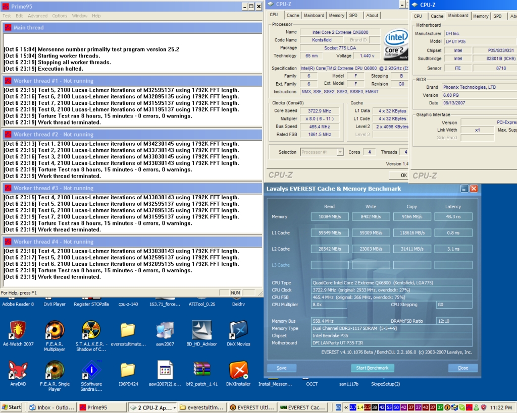
This swap to water-cooling allowed us sufficient temperature overhead to run Prime95 type tests for 11 hours with speeds of 3.72GHz @ 465FSB on the 333 strap with 4GB of RAM, while holding 470FSB on the 266 strap and 2GB of memory stable at around 467FSB. A 5-7 FSB margin above Prime95 type testing is often usable for those who do not require absolute 100% load stability to find sleep at night.
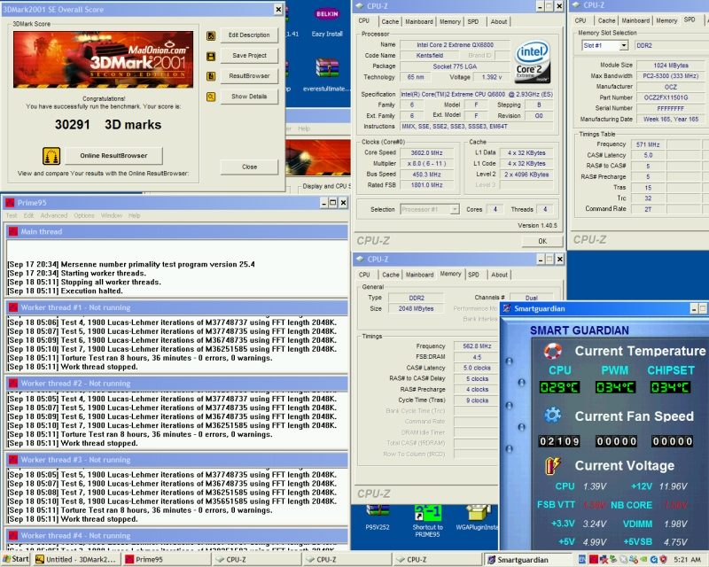
Prime95 and Everest
 |
We found that CPU scores in 3DMark06 using the DFI P35 T2R were higher than we were accustomed to on the acclaimed 975X chipset. We managed to push 4GB of RAM to 490FSB with water-cooling for a quick run of 3DMark06. The board at this point however was right on the ragged edge and would not run SuperPi 32M without a failure.
 |
Benchmark Performance Comparisons
Next, we wanted to look at the performance of various FSB/divider combinations with 2GB/4GB of RAM. We decided to stick with our tuned 465FSB 1333/800 strap overclock, comparing results between lower FSBs on the 266 strap whilst retaining around 3.72GHz of CPU speed. Any assessments within this section are scrutinized upon the principle of lowest voltages for stable operation at the most effective performance point.
With 4GB of memory in place and the 266 strap we used a Performance Level of 6 when clocking over 400FSB. We used the 266/667 combo@ 414FSBx9 to mimic the CPU speed of 465x8 using the 333/800 divider. Although there is an obvious memory speed disadvantage using the 266/667 combination, justification for doing so was the low VDimm we used for the 465FSB overclock: only 2.12 VDimm was required. While 5-4-4 timings @ 1034MHz using the 266/667 combination demanded around 2.2 VDimm, both are reasonable enough for long-term everyday use.
Using the 266/800 divider would have set the memory speed well in excess of 1200MHz, which quite frankly would require outside warranty specification voltages to operate, including higher VNB to even benchmark the board.
All 3D benches/comparisons were run with an NVIDIA 8800 Ultra clocked at 692/1205
4GB RAM And 333/800 Strap Benchmarks
3DMark01
.jpg) |
3DMark06
.jpg) |
Company of Heroes 1920x1200
.jpg)
Company of Heroes 1280x1024
.jpg)
Cinebench R10
.jpg) |
SuperPi 32M
.jpg) |
4GB RAM and 266/667 Strap Benchmarks
3DMark01
.jpg) |
3DMark06
.jpg) |
Company of Heroes 1920x1200
.jpg)
Company of Heroes 1280x1024
.jpg)
Cinebench R10
.jpg) |
SuperPi 32M
.jpg) |
2GB 266 Strap Benchmarks
3DMark01
.jpg) |
3DMark06
.jpg) |
Company of Heroes 1920x1200
.jpg)
Company of Heroes 1280x1024
.jpg)
Cinebench R10
.jpg) |
SuperPi 32M
.jpg) |
Choosing an operating point
Looking at the figures shown one could ask, is all the tweaking worth it? Benchmarking performance with the various configurations of FSB/divider and memory timings is remarkably close. For gaming systems it is perfectly acceptable to use around 400-430 FSB on the 266 strap, as frame rates are not adversely affected by the FSB deficit.
Obviously those who enjoy benchmarking will prefer the potential of higher bandwidth, as sensitive benchmarks like SuperPi 32M and 3DMark 2001SE can take advantage of the extra tweaks the board offers to maintain low access latency along with high FSB speeds. Running high FSBs on last generation chipsets usually resulted in fairly apparent performance losses, which at times could even be overcome with lower CPU speeds while using a tighter chipset strap. DFI's implementation of the P35 chipset maintains bandwidth scaling if the relevant BIOS tweaks are applied.
It is clear that modern gaming engines are not as dependent on outright CPU/RAM performance tuning, certainly not to the level many of us tweakers would like to believe. The most important factor with Intel Core 2 processors still revolves around the 266/333 straps and actual CPU MHz speed for noticeable gains in overall gaming performance. Luckily enough, those using Q6600 CPUs have the option of the 9x multiplier, allowing us to overclock to the limits of current air/water-cooling capacity quite easily without the need to spend large amounts of time chasing higher FSBs of little visible gain.
Another positive here is that 4GB overclocking with the right modules is actually a lot easier than we are accustomed to on previous chipsets. Attaining higher RAM speeds with tighter sub-timings almost feels akin to overclocking 2GB of RAM rather than 4GB. Obviously XP 32-bit will not take full advantage of the additional 2GB of RAM. Vista 64-bit testing is underway to study the variance between how the board reacts to a true 4GB load.
Going Sub-Zero With Our Cascades
Hardware used:
PCP&C 1200W PSU
2GB OCZ Flex 9200 RAM
ASUS 8800 GTS 640MB
WD2500 KS 250GB Hard Drive
Intel X6800 Core 2 Duo CPU (Retail)
Dual Rotary Cascade (CPU cooling)
Dual Mini Cascade (GPU cooling)
Dimas Tech Benching Table
Moving over to sub-zero means that all voltage related conservatism was thrown out of the window, as evaporator loaded temps remained between -110 and -106C throughout testing. Due to the clean CPU socket area, neoprene insulation can be applied with relative ease, one issue with Digital PWM is that all the heat producing components are aligned on one side of the socket (to the left). Obviously due to a lack of heat producing circuitry around the top side of the socket, the associated area is very prone to condensation during extended benchmarking sessions, we recommend you take a little extra time checking insulation is sufficient enough to prevent any moisture penetration.
The initial plan was to scale up the settings which had worked well when benching the water-cooling setup with the QX6800. We had not accounted for the fact that our QX6800 was reluctant to run over 4.5GHz in both four and two core mode. It was taking copious amounts of time to try and hold the board steady with the QX6800 (both in two and four core mode) anywhere over 4.5GHz. We eliminated all possibilities of PSU based inadequacies by comparing clocking results on two separate models and also cross comparing motherboards by using the ASUS Striker Extreme.
Both boards exhibited the same CPU MHz wall, so it was time to move on to another processor. One other oversight is that we should have used an air-cooled graphics card while we were attempting to tweak GTL settings. The 8800 GTS was also being cascade cooled, and idle temps were hovering in the region of -81C. The side effect of leaving the card idling while trying to improve the CPU stability was that the whole graphics card froze over - lesson learned.
After a few hours of various attempts with several processors, our trusty Core 2 Duo X6800 was dusted off and given the thumbs up for a test run. After spending the better part of a day tweaking and twisting BIOS settings, we did manage to save a few screenshots with the X6800.
.jpg) |
.jpg) |
.jpg) |
The 8800 GTS 640MB card clocked up really well at 940MHz on the core with around 1.55Vgpu while our X6800 ran without fault at these settings. It has to be said that the whole benchmarking experience, while tiring, was thoroughly enjoyable. Kudos to the folk who are able to manage LN2 on a couple of pots while trying to break records! Going sub-zero is not as easy as one would initially think. We will endeavor to provide more testing like this in the future on performance oriented motherboards with a standard set of peripherals; although the sacrifice in time is great, the end results are very rewarding and certainly a fun experience.
Conclusion
We have found our experience with the DFI UT P35-T2R quite pleasurable. The pre-release testing regimen used by DFI has obviously paid dividends in reducing general hardware and software incompatibility issues. DFI has been quick to respond to any concerns or questions that we have posed through a variety of means. We see good communication being pivotal to any form of success and it is always promising when manufacturers are willing to listen to the user base.
One looming subject has been the poor overclocking of Micron D9GKX based memory. It is now believed the P35 chipset itself is the weak link, rather than motherboard or even memory module PCB layout issues. Our own tests have revealed that these top-binned modules do seem to require additional voltage at just about any speed to remain stable - this goes for all P35 based motherboards.
Otherwise, the layout and performance of this board has been nearly perfect over the past few weeks. So much so, that we have little trouble in recommending this board to the enthusiast who is willing to get down and dirty with the BIOS in order to properly tune this board for exceptional performance results. The one potential flaw, or its Achilles' heel, is a price that nears $300 in most markets. This board will return performance that some would argue is worth its asking price; for us, the price is just a little over the top and is not for the faint of heart nor for people on a budget.
 |
Logic aside, there has been a growing market for advanced BIOS overclocking functions over the last few years. Those who have been loyal to the DFI brand expect no less than a plethora of BIOS options and this board does deliver in that regard. As the benchmark test runs have shown, only those chasing crucial seconds or point advantages for outright benchmarking truly notice the difference of higher FSB speeds, though this does not appear to diminish the demand from users to see future products from DFI with similar performance based options. The added flexibility of manipulating BIOS settings to overcome strap change latency loss may well be paving the way for the next generation of processors and chipsets.
The latest DFI A05 beta BIOS has added support for 45nm CPUs. Of further interest still is that the default multipliers on some of the lower end quad-core CPUs will be locked at seven, demanding motherboards with high FSB potential to acquire the raw CPU speeds that the 45nm process should be capable of (if Intel does not speed bin the lower range heavily). Rest assured, we will need BIOS options to retain performance as FSB is scaled even higher.
With X38 based motherboards entering the market now, it would seem the long-term potential for enthusiast level P35 boards is diminished. However, we feel there is still plenty of life left in DFI's new toy, especially since overclocking on the latest X38 motherboards does not match the clocking ability of this motherboard at present. Over the next few months the FSB abilities of Intel's P35 chipset with upcoming CPUs will determine just how long this line of P35 motherboards will remain desirable.


