Original Link: https://www.anandtech.com/show/1044
nForce2 6-way Motherboard Roundup - December 2002
by Evan Lieb on December 4, 2002 6:53 PM EST- Posted in
- Motherboards
Today we're taking a look at a roundup of six motherboards based on NVIDIA's latest chipset, the nForce2. With the original nForce already established as a solid and speedy solution among enthusiasts and OEMs alike, NVIDIA is merely trying to improve upon their first generation chipset with nForce2.
Indeed, nForce2 has shown to be the fastest Athlon XP chipset currently available on the market. For more information and in depth coverage of nForce2, take a look at our previous articles:
-
For information about the nForce2 technology, read our technology overview.
- For nForce2 performance, read the latest part of our nForce2 coverage.
We won't delay you any further with chitchat, so read on to find out more about six retail nForce2 motherboards…
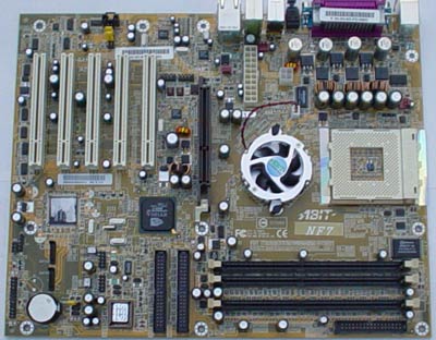
ABIT NF7-S Version 1.0: Basic Features
|
Motherboard Specifications |
|
|
CPU
Interface
|
Socket-462
|
|
Chipset
|
NVIDIA
SPP North Bridge
NVIDIA MCP-T South Bridge |
|
Bus
Speeds
|
100
- 237MHz (in 1MHz increments)
|
|
Core
Voltages Supported
|
up
to 1.85V (in 0.025V increments)
|
|
I/O
Voltages Supported
|
N/A
|
|
DRAM
Voltages Supported
|
up
to 2.7V in 0.1V increments
|
|
Memory
Slots
|
3
184-pin DDR DIMM Slots
|
|
Expansion
Slots
|
1
AGP 8X Slot
5 PCI Slots |
|
Onboard
ATA RAID
|
N/A
|
|
Onboard
USB 2.0/IEEE-1394
|
USB
2.0 supported through South Bridge
Realtek RTL8801B FireWire PHY (MAC in South Bridge) |
|
Onboard
LAN
|
Realtek
RTL8201BL controller (nForce LAN)
|
|
Onboard
Audio
|
Realtek
ALC650 controller (nForce2 APU)
|
|
Onboard
Serial ATA
|
Silicon
Image 3112A RAID controller
|
|
BIOS
Revision
|
nf7_11.b01
(11/25/2002)
|
Despite the fact that ABIT's NF7-S isn't a MAX series motherboard, the NF7-S still packs an acceptable punch. Besides, it's hard to argue that nForce2 isn't the most fully-featured Socket A chipset on the market, so some may not even mind that ABIT skipped MAX for their nForce2 series of motherboards.
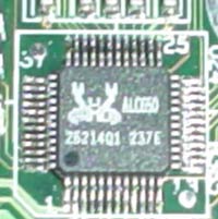
In order to take advantage of NVIDIA's nForce2 Ethernet, ABIT has outfitted the NF7-S with a Realtek 8201BL Ethernet PHY. The RTL8201BL is the physical layer for the nForce MAC integrated into the MCP-T; it is interesting to note that ABIT did not take advantage of the dual integrated MACs in the MCP-T, unlike ASUS.
Yet another feature Realtek seems to dominate are sound controllers, this time in the form of their ALC650 chip, which can be found just below the NF7-S' I/O ports, and which handles all sound output for the board. Remember that the nForce2 APU only acts as a DSP, final sound quality is still greatly determined by the DAC (Digital to Analog Converter) in the ALC650 AC'97 codec.
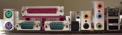
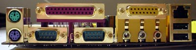
The I/O ports aren't configured in an especially interesting way; Here you'll find two PS/2 ports, two serial ports, one parallel port, two rear USB 2.0 ports, one LAN port, a SPDIF port, and five 1/8' jacks, which are driven by the onboard sound. Nothing exciting to note here, as this is pretty standard among nForce2 motherboards.
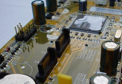
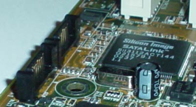
Silicon Image's SI3112A Serial ATA RAID controller has recently started to become popular among high-end and high-performance motherboards, including ASUS's P4G8X Deluxe (Intel E7205 chipset), Intel's D845PEBT2 (Intel 845PE chipset), Epox's 4PEA+ (Intel 845PE chipset), and ECS's L4S8A (SiS 648 chipset). With this onboard Serial ATA chip, you can setup two independent Serial ATA devices as well as RAID 0 (striping) and RAID 1 (mirroring) arrays. Onboard Serial ATA, in our opinion, is a nice perk, but nothing more. Serial ATA drives are finally trickling into the market but you won't see widespread support until SATA controllers are integrated into South Bridges in 2003.
The ABIT NF7-S doesn't support a large number of IDE devices, certainly nothing too interesting. The Primary and Secondary IDE connectors form the only type of onboard IDE support, supporting two channels per IDE connector. Therefore, the NF7-S supports no more than four IDE drives total, which really shouldn't be an issue with the vast majority of users (and yes, even power users).
The MCP-T South Bridge supports USB 2.0, or up to six USB 2.0 ports total. Besides the two rear USB 2.0 ports, there are two USB 2.0 headers located towards the bottom of the NF7-S. Here you'll be able to add a maximum of four USB 2.0 ports through whatever means you deem fit (using the bundled two-port USB bracket or otherwise).
For some, the NF7-S' support for FireWire is a plus, thanks to the integrated FireWire MAC in the nForce2 MCP-T.
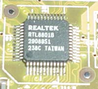
ABIT bundles a two-port FireWire bracket with the NF7-S for you to use with the two onboard FireWire headers. Since the RTL8801B controller can support no more than two FireWire ports, the bundled FireWire bracket is especially useful.
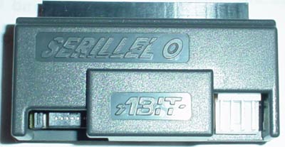
ABIT has been trying to separate themselves from other motherboard manufacturers as much as possible lately. This goal couldn't be better exemplified than by their Serillel converter technology. Essentially, the Serillel converter converts an IDE hard drive into a serial ATA hard drive just by converting the parallel signal from the IDE hard drive to a serial signal. The current advantage of Serillel is that you can add an additional IDE drive to your system (for a total of five instead of four). This seems nice, but remember that there will be some performance loss because of the Parallel to Serial conversion; on paper the performance loss shouldn't be too great but we'll be investigating that in the coming weeks.
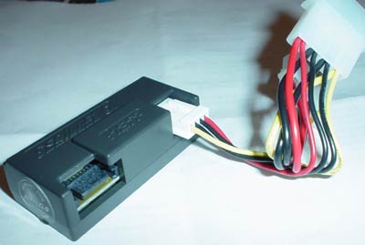
One positive of ABIT's Serillel converters is that you get the benefit of Serial ATA cables without having to wait for Serial ATA hard drives to hit store shelves.
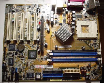
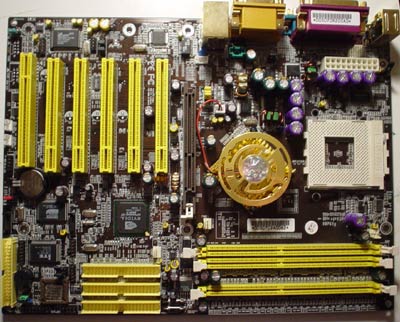
ABIT NF7-S: Board Layout
Luckily enough, there weren't too many layout issues to point out with the ABIT NF7-S.
We really weren't too keen on the positioning of the ATX (20-pin) connector on the ABIT NF7-S. Instead of being on the left-hand side of the motherboard, we would have preferred to have seen it located on the right-hand, upper portion of the motherboard. This is the best place to position an ATX connector, as the thick wires won't obstruct the installation/uninstallation of the CPU's heatsink.
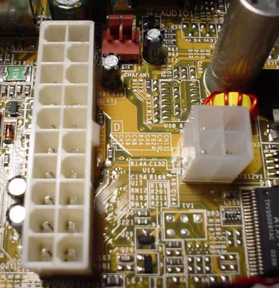
Oddly enough, the ABIT NF7-S had an AT12V connector located on its PCB. We've seen maybe two Athlon XP motherboards with an ATX12V connector in the past. We wonder what the purpose of this connector is for Socket A, considering AMD hasn't set any new guidelines as far as needing to implement ATX12V to feed enough juice to the CPU; though, as the Athlon ramps up, this may be inevitable.
One feature we felt ABIT shouldn't have missed was the four mounting holes around the CPU socket that are so vital to all those Swiftech and Alpha users and cooling fanatics in general. However, the official word from ABIT is that the NF7-S will indeed ship with four mounting holes even though our sample didn't have this feature. Admin and owner of Hexus.net, David Ross, was good enough to alert us to this fact. 12-10-02 UPDATE Apparently, the first few thousand NF7-S motherboards will ship without the mounting holes.
The Primary and Secondary IDE connectors are annoyingly positioned below where our video card is installed. Placing the Primary and Secondary IDE connectors this way makes it difficult for the IDE cables to reach the uppermost bays of a full-sized ATX case. There's a good chance the IDE cables will get tangled up with the video card as well, especially since the IDE connectors are placed horizontally instead of vertically on the motherboard.
Too many motherboard makers like to place the DIMM connectors right next to the video card. Unfortunately, ABIT is one of those motherboard makers with the NF7-S. The DIMM connectors are basically impossible to unhinge unless you go through the hassle of unscrewing and then physically uninstalling your video card just to throw in a stick of memory. For those that are picky about memory and frequently like to install different types of modules, the DIMM connector's position will be an annoyance. However, this won't be an issue with video cards that are shorter in length than our ASUS GeForce4 Ti4600.
The USB and FireWire headers are positioned fairly well. There are two USB 2.0 headers located near the bottom of the NF7-S PCB, but not quite far enough to our liking. The way these USB headers are positioned makes it difficult if you decide to use the onboard Serial ATA connectors for a future SATA hard drive or something. Despite the small size of Serial ATA cables, USB bracket cables can still overlap them and this just causes a mess.
ABIT NF7-S: BIOS and Overclocking
ABIT utilizes their own modified BIOS, dubbed Soft Menu III. Soft Menu III has been a huge hit among enthusiasts, so we had high hopes for ABIT's nForce2 BIOS.
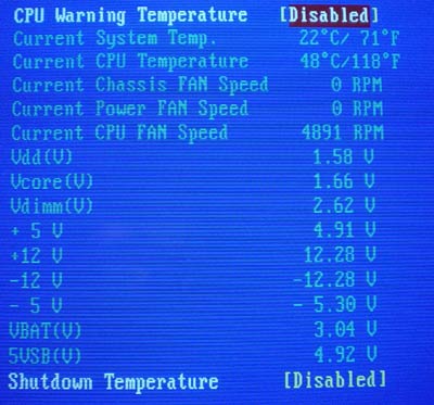
The Winbond W83627HF I/O chip powers the PC Health section of the Soft Menu III BIOS.
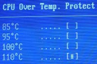
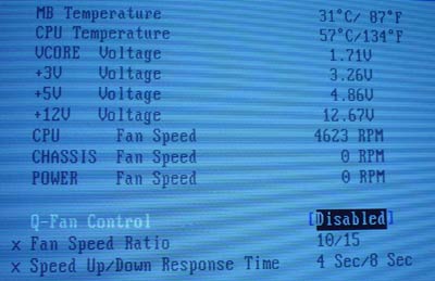
You'll find lots of readings in the PC Health section of Soft Menu III, including System and CPU temperatures, fan speeds (CPU, chassis and power), Vcore, PSU readings (all rails), and battery and standby voltage readings. In addition to the PC Health readings, you'll find options for enabling CPU shutdown temperature and adjusting CPU warning temperature. All in all, this is a common hardware monitor to have for a high-performance motherboard.
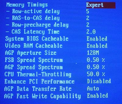
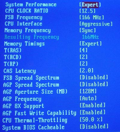
The Advanced Chipset Features section doesn't contain as many options as the other nForce2 BIOSes do, but this can be attributed to the fact that this is the only Advanced Chipset Features section of the nForce2 BIOSes that has been significantly modified from NVIDIA's original Advanced Chipset Features layout. ABIT does this by separating the DRAM timings from all other frequency adjustment options (including FSB, memory, etc.).
The Advanced Chipset Features section contains options for adjusting Precharge to Active, Active to Precharge, Active to CMD, and CAS Latency among other minor adjustments. Interestingly enough, the Active to Precharge timing can be adjusted as low as 1T, and up to 15T in fact. Though it's obviously not possible to get to 1T, we were able to go as low as 4T.
What's unique about nForce2 BIOSes versus VIA, SiS and Intel BIOSes is the "CPU Interface" option, which can either be enabled or disabled. Enabling CPU Interface does add some noticeable performance as far as actual benchmark numbers are concerned, but the real world difference is nonexistent. We actually first saw this "feature" on NVIDIA's reference board, which indicated that it simply tuned FSB performance. We saw no degradation of stability in any of our tests but again, the performance increase is only there in the benchmarks and isn't really tangible to end users so enable it at your own risk.
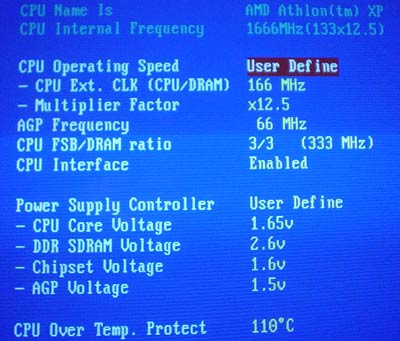
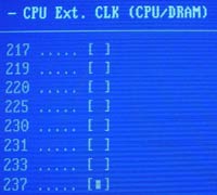
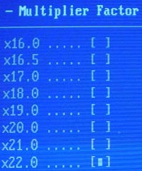
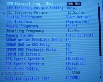
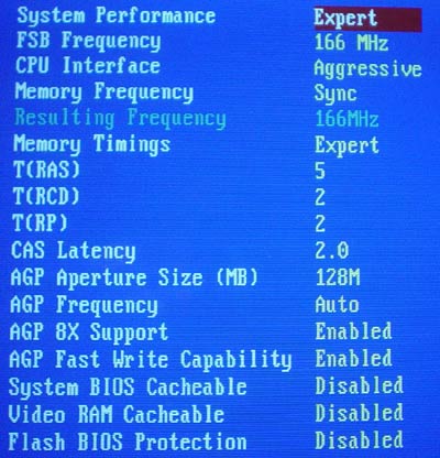
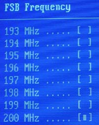
The "Soft Menu III" section listed at the very top of the NF7-S BIOS contains all the frequency adjustments you would normally find in the Advanced Chipset Features section of other nForce2 motherboard BIOSes. In "Soft Menu III" you'll find options for tweaking the FSB up to 237MHz in 1MHz increments, AGP up to 99MHz in 1MHz increments, multipliers ranging from 5X to 22X, FSB/DRAM dividers, and of course the CPU Interface. As is common with nForce2 BIOSes, there are "Optimal" and "Aggressive" options that automatically adjust various settings in the Advanced Chipset Features section. However, we suggest you simply select the "Expert" option for full customization, assuming you have some experience with BIOS tweaking.
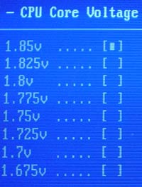
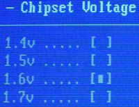
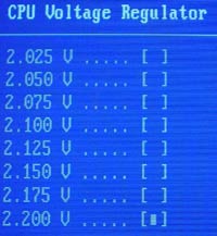
There are also some fairly nice voltage options buried inside the Soft Menu III section. For example, Vcore is adjustable in .025V increments all the way up to 1.85V. This maximum Vcore isn't all that great, especially if you plan on using a .18-micron Palomino processor (whose default Vcore is 1.75V). However, Thoroughbred-B users should do quite well with a max of 1.85V, especially since running your CPU higher than 1.85V can be detrimental to the longevity of the CPU's lifespan.
 |
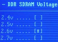 |
VDIMM is yet another adjustable option in the Soft Menu III section. VDIMM can be altered up to 2.7V in 0.1V increments, which is just fine for most users. Memory overvolting usually doesn't yield too much better of a memory overclock anyways, so there's nothing to worry about there.
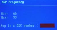
The NF7-S BIOS version we received contained an AGP lock set at 66MHz, but we were unable to find any PCI lock set at 33MHz in this BIOS. We asked ABIT why the AGP lock was included in the NF7-S BIOS but not the PCI lock, and we were basically told that the only reason you don't see a PCI lock in the BIOS is because ABIT doesn't want users fooling around with PCI frequency, especially since it offers virtually no performance gain. We don't have any way of independently verifying ABIT's PCI lock claim ourselves, so take this piece of information as you will.
As with all the nForce2 motherboards tested here today, it was very easy to overclock the NF7-S. Here were our FSB overclocking results using the following setup:
|
Front Side Bus Overclocking Testbed |
|
|
Processor:
|
Athlon
XP 2400+
|
|
CPU
Vcore:
|
1.65V
|
|
Cooling:
|
AMD
Retail HSF & Thermal Pad
|
|
Power
Supply:
|
Enermax
300W
|
With this very common, and therefore quite conservative, overclocking setup we were able to hit 186MHz FSB. This is a very good overclock and is the norm for all nForce2 boards tested here today.
We'd quickly like to mention something before we go on. The great thing about Athlon XP processors is that they can be unlocked (unlike modern-day Intel CPUs), and being able to unlock a processor is a boon for computer hardware review sites such as AnandTech, as it gives us the ability to test the true maximum FSB a particular motherboard can handle.
For our overclocking tests on the NF7-S, we simply lowered the multiplier of our 2400+ processor down to 8X and jacked up the FSB as high as we could, which ended up being 186MHz FSB in the NF7-S' case (or 186MHz X 8.0).
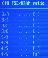
The divider options available in the NF7-S BIOS are very good; quite a few memory tweakers should be delighted to see the huge array of memory dividers options available on this motherboard. Just some of the many available memory divider options include 4:5, 3:4 and 1:1. For a more complete list, see the above picture.
ABIT NF7-S: Stress Testing
There is quite a bit a stress testing potential with this nForce2 motherboard due to the abundant amount of BIOS options available. We managed to test the NF7-S in several different areas and configurations, including:
1. Chipset and motherboard stress testing was conducted by running the FSB at 186MHz.
2. Memory stress testing was conducted by running RAM at 333MHz and 400MHz with as many modules populated as possible at the most aggressive timings possible.
Front Side Bus Stress Test Results
At 186MHz FSB we were able to run the NF7-S beautifully. As usual, we ran 24 hours straight of Prime95 torture tests at 186MHz FSB before we decided the NF7-S was reliable enough for our liking for the time being. We also ran some other apps while Prime95 was crunching away, which included various DX8 games (JKII, etc.), data compression, and light apps like Word and Excel. With the little time we had left we ran a few more benchmarks a second time, including SPECviewperf 7.0, Sciencemark and XMPEG. Still, we couldn't faze the NF7-S at 186MHz FSB. We should note that 187MHz FSB was very stable as well, though we did encounter a crash in SPECviewperf once.
Memory Stress Test Results
This first memory stress test is quite a challenge for some so-called "DDR333" motherboards, but the nForce2-powered ABIT NF7-S is easily able to handle this particular scenario. Here were the timings we were able to achieve:
|
Stable
DDR333 Timings |
|
|
Clock
Speed:
|
166MHz
|
|
Timing
Mode:
|
N/A
|
|
CAS
Latency:
|
2
|
|
Bank
Interleave:
|
N/A
|
|
Precharge
to Active:
|
2T
|
|
Active
to Precharge:
|
4T
|
|
Active
to CMD:
|
2T
|
|
Command
Rate:
|
N/A
|
These are very aggressive timings. What stands out the most is the Precharge to Active setting, which is lower than we've ever been able to run any motherboard before. In case you're wondering, the "CPU Interface" option was enabled during this stress test.
This final memory stress test tests how high (up to no more than 400MHz) the NF7-S can run three memory modules at the timings listed below. Here were our results:
|
Stable
DDR400 Timings |
|
|
Clock
Speed:
|
200MHz
|
|
Timing
Mode:
|
N/A
|
|
CAS
Latency:
|
2
|
|
Bank
Interleave:
|
N/A
|
|
Precharge
to Active:
|
2T
|
|
Active
to Precharge:
|
4T
|
|
Active
to CMD:
|
2T
|
|
Command
Rate:
|
N/A
|
Running at 400MHz, these are great timings when you consider that all memory banks are filled and fully operational. These are the best timings we've seen yet for three DIMMs running at 400MHz.
Memory overclocking on the NF7-S wasn't particularly spectacular. We experienced similar results with other nForce2 boards as well. Still, the results aren't too shabby:
|
Stable
Memory Overclocking Results |
|||
|
Memory
|
Memory
Clock
|
FSB
|
VDIMM
|
|
Corsair
CAS2.0 DDR400
|
412MHz
|
165MHz
|
2.6V
|
These are nice numbers, especially at the timings listed. Even when we did back off on the aggressive timings though, stability over 412MHz wasn't possible.
As we always do, we ran a bunch of tests to make sure our memory timings and overclocks were stable. We started off by running Prime95 torture tests; a grand total of 24 hours of Prime95 was successfully run at the timings listed in the above charts. We also ran Sciencemark (memory tests only) and Super Pi. None of the stress tests were able to bring the NF7-S to its knees.
SoundStorm Stress Test Results
We ran the same sound tests on the NF7-S as we did with all the other nForce2 motherboards tested here today. The following demos were run with SoundStorm enabled:
1. Jedi Knight II: Passed
2. Quake 3 Arena: Passed
3. Unreal Tournament 2003: Passed
4. Comanche 4: Passed
5. Serious Sam: Passed
There have been some minor, ongoing issues with NVIDIA's nForce1 APU drivers since the nForce1's introduction last year. Some users have experienced a Blue Screen of Death with nForce sound enabled in games like Unreal Tournament. However, the latest nForce2 unified driver package (v 2.00) has seemingly fixed the sound issues that nForce1 users were experiencing. This is backed up by our own test results, which show that SoundStorm is able to smoothly play five of some of the most popular games out there, including Unreal Tournament.
ABIT NF7-S: Tech Support and RMA
For your reference, we will repost our support evaluation procedure here:
The way our Tech Support evaluation works is first we anonymously email the manufacturer's tech support address(es), obviously not using our AnandTech mail server to avoid any sort of preferential treatment. Our emails (we can and will send more than one just to make sure we're not getting the staff on an "off" day) all contain fixable problems that we've had with our motherboard. We then give the manufacturer up to 72 hours to respond over business days and will report not only whether they even responded within the time allotted but also if they were successful in fixing our problems. If we do eventually receive a response after the review is published, we will go back and amend the review with the total time it took for the manufacturer to respond to our requests.
The idea here is to encourage manufacturers to improve their technical support as well as provide new criteria to base your motherboard purchasing decisions upon; with motherboards looking more and more alike every day, we have to help separate the boys from the men in as many ways as possible. As usual, we're interested in your feedback on this and other parts of our reviews so please do email us with your comments.
ABIT's RMA policy is a very unique one among motherboard makers. You can take a look at ABIT's U.S. RMA policy, aptly dubbed eRMA (Express RMA) here.
ABIT's eRMA guarantees two critical things that most other motherboard makers are too shy or unwilling to make:
1. ABIT clearly explains that they will accept and process direct RMAs.
2. ABIT guarantees a 10-day turnaround policy on all RMAed motherboards.
ABIT's RMA and warranty information are also easily accessible on their U.S. web site by simply clicking the eRMA hyperlink at the left-hand corner of the page and cycling through each category. All in all, ABIT has done a great job making their RMA and warranty information easily available and understandable on their web site, which is a huge advantage over other top tier motherboard manufacturers.
ABIT's tech support isn't as impressive as far as available information on their web site. However, there is an email address you can use if you need to write to tech support, which is [email protected]. You can also reach ABIT in the U.S. by phone at (510) 492-0968 as well. Their hours are pretty good too; 9:00am to 6:00pm (although ASUS's phone hours are a bit better in the U.S.).
As far as email tech support response time was concerned, we were delighted to see ABIT reply so quickly, clocking in at 22 hours. Tech support was friendly and very helpful in general, and they indeed answered our question correctly. All in all, it was a good experience, especially knowing that they took less than a day to reply.
ABIT's RMA policy is unmatched in the U.S.; no other motherboard manufacturer comes close. In combination with their timely tech support reply, we feel ABIT is one of the best (if not the best) motherboard manufacturer to turn to for motherboard customer service and support in the U.S.
ASUS A7N8X Deluxe: Basic Features
|
Motherboard Specifications |
|
|
CPU
Interface
|
Socket-462
|
|
Chipset
|
NVIDIA
SPP North Bridge
NVIDIA MCP-T South Bridge |
|
Bus
Speeds
|
100
- 211MHz (in 1MHz increments)
|
|
Core
Voltages Supported
|
up
to 1.850V (in 0.025V increments)
|
|
I/O
Voltages Supported
|
N/A
|
|
DRAM
Voltages Supported
|
up
to 2.7V in 0.1V increments
|
|
Memory
Slots
|
3
184-pin DDR DIMM Slots
|
|
Expansion
Slots
|
1
AGP 8X Slot
5 PCI Slots |
|
Onboard
ATA RAID
|
N/A
|
|
Onboard
USB 2.0/IEEE-1394
|
USB
2.0 supported through South Bridge
Realtek RTL8801B FireWire PHY (MAC in South Bridge) |
|
Onboard
LAN
|
Realtek
RTL8201BL controller (nForce LAN)
|
|
Onboard
Audio
|
Realtek
ALC650 controller (nForce2 APU)
|
|
Onboard
Serial ATA
|
Silicon
Image 3112A RAID controller
|
|
BIOS
Revision
|
1003
|
The ASUS A7N8X is part of ASUS's series of Deluxe motherboards. There is another stripped down version of the A7N8X without Serial ATA, dual LAN, SoundStorm and FireWire.
Much like ABIT, ASUS used the RTL8201BL physical layer to implement the nForce2's integrated Ethernet. ASUS went one step further and included a second PHY, the Altima AC101L to provide dual LAN functionality driven by the MCP-T's integrated 3Com MAC.
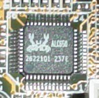
Again, it's no surprise to see that the Realtek ALC650 is used on the A7N8X. Remember that the nForce2 APU only acts as a DSP, final sound quality is still greatly determined by the DAC (Digital to Analog Converter) in the ALC650 AC'97 codec.
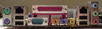
ASUS sets up the I/O configuration in an interesting way. Here you'll find two PS/2 ports, one serial port, one parallel port, four rear USB 2.0 ports, two LAN ports, and six 1/8' jacks, which are driven by the onboard sound. Each LAN port is powered by a different MAC; the LAN port closest to the PS/2 ports is powered by 3Com's 3C920B MAC, while the LAN port situated on the other side of the I/O ports is NVIDIA's own Ethernet MAC.
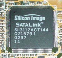
The ASUS A7N8X Deluxe is yet another motherboard that uses Silicon Image's SI3112A Serial ATA RAID controller.
Other high-performance motherboards that include this onboard Serial ATA RAID controller include ABIT's NF7-S (NVIDIA nForce2 chipset), ASUS's P4G8X Deluxe (Intel E7205 chipset), Intel's D845PEBT2 (Intel 845PE chipset), Epox's 4PEA+ (Intel 845PE chipset), and ECS's L4S8A (SiS 648 chipset). The SI3112A controller lets you setup two independent Serial ATA devices as well as RAID 0 (striping) and RAID 1 (mirroring) arrays.
The A7N8X Deluxe doesn't support as many IDE devices as we have seen on other motherboards in the past. This is due to the fact that the A7N8X Deluxe doesn't come with more than just one Primary IDE connector and one Secondary IDE connector, both of which offers two channels each for a maximum of four possible IDE devices (for example, two hard drives and two optical drives). But as we mentioned before, it is rare for users to take advantage of more than 4 IDE devices so this isn't really a downside.
IDE RAID would have been a nice addition to this motherboard, though we're sure the A7N8X Deluxe wouldn't be as much of a bargain; currently, you can purchase the ASUS A7N8X Deluxe for about $140 online in the U.S.
The MCP-T South Bridge supports USB 2.0, six USB 2.0 ports altogether. There are two USB 2.0 headers located at the bottom, right-hand corner of the A7N8X Deluxe. Just plug in the USB 2.0 bracket that comes bundled with this motherboard into one of the two onboard USB headers and you can have six USB 2.0 ports if you so desire.
Onboard FireWire support is controlled by Realtek's RTL8801B, which supports up to two FireWire ports. You can connect the FireWire bracket that comes bundled with this motherboard into the two white FireWire headers located on the left-hand side of the motherboard, next to the 3rd PCI slot.
ASUS A7N8X: Board Layout
There were very few layout issues with the ASUS A7N8X. This nForce2 motherboard had one of the better layouts for the most part.
Looking at the positioning of the ATX (20-pin) connector, we see that ASUS placed it on the right-hand side of the motherboard. This is the best place to position an ATX connector, as the thick wires won't obstruct the installation/uninstallation of the HSF or passive North Bridge heatsink, as well as any other components that you may decide to modify or uninstall. Unfortunately, the ATX connector isn't located high enough; the ideal position would be at the very top, right-hand corner of the motherboard, perhaps just over the DIMM slots.
We're glad that ASUS places the Primary and Secondary IDE connectors to the right of the DIMM slots and just above the midsection of the motherboard. We've experienced what a hassle it can be to have the Primary and Secondary IDE connectors placed on the lower portion of the motherboard. It makes it more difficult for the IDE cables to reach to the uppermost bays of a large-sized ATX case, which can get tangled up with the video card.
There are a lot of motherboard makers that place their DIMM connectors too close to where the video card is installed. However, ASUS doesn't make this mistake, and places their DIMM connectors far enough away from our GeForce4 Ti4600 and with a fair amount of room to spare, as is apparent from the motherboard picture in the previous section. We always like it when mainboard manufacturers do this because we're not forced to uninstall the video card if we want to uninstall memory, which is a common occurrence for people who upgrade frequently.
The USB and FireWire headers are positioned fairly well. There is one lone USB header located at the bottom of the board, right where it should be. There are also two (white) FireWire headers located on the left-hand side of the motherboard, right next to the RTL8801B controller. The FireWire header position isn't as good, since the bracket wires will get in the way of other PCI cards (assuming you decide to install one).
ASUS A7N8X: BIOS and Overclocking
ASUS has always used their own unique BIOS format, though the A7N8X BIOS is still based on Phoenix Technology's Award BIOS.
There is a good deal of readings available in the A7N8X Hardware Monitor portion of the BIOS.
These readings include CPU and motherboard temperatures, Vcore, PSU readings (all rails), three different fan speed readings (CPU, chassis, power), and ASUS's very own patented Q-fan control, which regulates your CPU fan speed based on how taxed your system is at any given moment. These are fairly basic readings for a high-performance BIOS, but it's quite acceptable nonetheless.
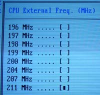
The Advanced Chipset Features section includes a fair amount of options. These include adjustments for FSB (up to 211MHz), CPU multiplier, memory frequency, various memory timings, Vcore, VAGP, and VDIMM. The picture above doesn't show the VAGP or VDIMM adjustments, but they're certainly there.
The A7N8X BIOS has some fairly decent voltage tweaking capability.
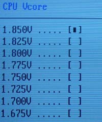
First off, Vcore is adjustable in .025V increments all the way up to 1.85V.
Like the NF7-S, this is pretty low for Palomino users, but we suggest you
use a Thoroughbred-B processor anyway, as a 0.2V increase in Vcore should
be more than enough for avid Thoroughbred overclockers. Running any higher
than 1.85V really isn't recommended, even with heavy-duty cooling setups.
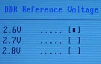
In the A7N8X BIOS you're able to adjust VDIMM up to 2.8V in 0.1V increments. Memory overclockers shouldn't have any trouble with this type of memory voltage availability, especially since we were able to get a decent memory overclock with VDIMM set at just 2.6V.
The A7N8X BIOS definitely does contain an AGP bus lock at 66MHz. However, what about the PCI bus lock at 33MHz? For this question we headed over to ASUS and asked them what was going on. ASUS's response was simply that they have a PCI bus lock set at 33MHz and that you have nothing to worry about as far as running your devices out of specification while performing FSB overclocking.
Overclocking the ASUS A7N8X Deluxe was very easy for the most part. Here were our FSB overclocking results using the following setup:
|
Front Side Bus Overclocking Testbed |
|
|
Processor:
|
Athlon
XP 2400+
|
|
CPU
Vcore:
|
1.65V
|
|
Cooling:
|
AMD
Retail HSF & Thermal Pad
|
|
Power
Supply:
|
Enermax
300W
|
We were able to reach 185MHz FSB (370MHz DDR) using this conservative overclocking setup. This overclocked FSB frequency is normal compared to the other nForce2 SPP motherboards we've tested here today.
Using a factory locked Athlon XP 2400+ processor, all we had to do was simply lower the CPU multiplier down to 8X and increase the FSB as high as we possibly could without jeopardizing stability and without increasing voltages. This was made possible by a great feature the ASUS A7N8X Deluxe affords (as do all nForce2 motherboards), and that's the ability to adjust the CPU multiplier in the BIOS without having to do physical modification to the CPU. Therefore, all you have to do is install your multiplier-locked Athlon XP CPU into your nForce2 motherboard and voila; you can adjust all the available multipliers to your heart's content. However, make sure you purchase the right type of Athlon XP; only Thoroughbred-B processors have this capability on nForce2 motherboards. You cannot change the multiplier of a locked Palomino or Thoroughbred-A processor in any of the six nForce2 motherboards being reviewed today.
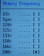
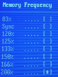
There also are lots of divider options available, exactly the same ones you'll see in most nForce2 BIOSes. You can adjust memory in many different ways, and as high as 400MHz if you'd really like to. See the above picture for more info.
ASUS A7N8X: Stress Testing
Since there is a good deal of dividers available in the A7N8X BIOS, we managed to test this board in several different areas and configurations, including:
1. Chipset and motherboard stress testing was conducted by running the FSB at 185MHz.
2. Memory stress testing was conducted by running RAM at 333MHz and 400MHz with as many modules populated as possible at the most aggressive timings possible.
Front Side Bus Stress Test Results:
The ASUS A7N8X ran like a charm at 185MHz FSB (370MHz DDR). We were able to make this assessment through 24 hours straight of Prime95 torture tests at this overclocked FSB speed. During the course of time Prime95 was running in the background, we also ran various DX8 games (JKII, etc.), light apps like Word and Excel, and data compression here and there, all with great success. In the past, rerunning benchmarks has shown to be an effective way of weeding out any minor stability bugs at a given overclocked frequency. In this case we reran SPECviewperf 7.0, Sciencemark and XMPEG. In all circumstances, running the FSB upwards of 370MHz DDR was very easy for the A7N8X. We were able to get even higher than 370MHz DDR, but two minor crashes left us unsatisfied.
Memory Stress Test Results:
In this first memory timings test we see how well the ASUS A7N8X is able to handle three memory modules installed and running at 333MHz DDR. Here were the timings we were able to achieve:
|
Stable
DDR333 Timings |
|
|
Clock
Speed:
|
166MHz
|
|
Timing
Mode:
|
N/A
|
|
CAS
Latency:
|
2
|
|
Bank
Interleave:
|
N/A
|
|
Precharge
to Active:
|
2T
|
|
Active
to Precharge:
|
4T
|
|
Active
to CMD:
|
2T
|
|
Command
Rate:
|
N/A
|
These are great timings. There won't be a single user out there that isn't satisfied with these aggressive timings. We must again note the lower Precharge to Active setting, which other motherboards (not based on nForce2) either cannot achieve or simply don't have the option of running at 4T. Also, remember that these timings were achieved with the CPU Interface enabled, which boosts performance a little.
Our final memory stress test shows how well the A7N8X is able to handle three memory modules running at 400MHz. Here were the timings we were able to achieve:
|
Stable
DDR400 Timings |
|
|
Clock
Speed:
|
200MHz
|
|
Timing
Mode:
|
N/A
|
|
CAS
Latency:
|
2
|
|
Bank
Interleave:
|
N/A
|
|
Precharge
to Active:
|
2T
|
|
Active
to Precharge:
|
4T
|
|
Active
to CMD:
|
2T
|
|
Command
Rate:
|
N/A
|
Again, we see absolutely stellar timings. It's important to note that these timings are hard to achieve if you aren't using the right type of memory. In our A7N8X tests, we used Corsair DDR400 CAS2 memory, which has always been able to handle aggressive timings such as these. Corsair is one of the few memory brands that able to achieve these timings at such a high memory frequency as 400MHz.
The A7N8X ended up being the best memory overclocker of the bunch, though only by 2MHz. Here were our memory overclocking results:
|
Stable
Memory Overclocking Results |
|||
|
Memory
|
Memory
Clock
|
FSB
|
VDIMM
|
|
Corsair
CAS2.0 DDR400
|
420MHz
|
159MHz
|
2.6V
|
Naturally, we ran a large array of stress tests to ensure all the timings and memory frequencies we were able to reach were stable and fully operational in general. This meant running many hours of Prime95 torture tests, 24 hours of which was completed successfully. We also successfully completed Super Pi stress tests as well as Sciencemark and XMPEG benchmark runs a second time. All in all, all our memory testing results listed in the above charts ran successfully and without issue during our stress tests.
SoundStorm Stress Test Results
We ran the same sound tests on the A7N8X as we did with all the other nForce2 motherboards tested here today. The following demos were run with SoundStorm enabled:
1. Jedi Knight II: Passed
2. Quake 3 Arena: Passed
3. Unreal Tournament 2003: Passed
4. Comanche 4: Passed
5. Serious Sam: Passed
There have been some minor, ongoing issues with NVIDIA's nForce1 APU drivers since the nForce1's introduction last year. Some users have experienced a Blue Screen of Death with nForce sound enabled in games like Unreal Tournament. However, the latest nForce2 unified driver package (v 2.00) has seemingly fixed the sound issues that nForce1 users were experiencing. This is backed up by our own test results, which show that SoundStorm is able to smoothly play five of some of the most popular games out there, including Unreal Tournament.
ASUS A7N8X: Tech Support and RMA
For your reference, we will repost our support evaluation procedure here:
The way our Tech Support evaluation works is first we anonymously email the manufacturer's tech support address(es), obviously not using our AnandTech mail server to avoid any sort of preferential treatment. Our emails (we can and will send more than one just to make sure we're not getting the staff on an "off" day) all contain fixable problems that we've had with our motherboard. We then give the manufacturer up to 72 hours to respond over business days and will report not only whether they even responded within the time allotted but also if they were successful in fixing our problems. If we do eventually receive a response after the review is published, we will go back and amend the review with the total time it took for the manufacturer to respond to our requests.
The idea here is to encourage manufacturers to improve their technical support as well as provide new criteria to base your motherboard purchasing decisions upon; with motherboards looking more and more alike every day, we have to help separate the boys from the men in as many ways as possible. As usual, we're interested in your feedback on this and other parts of our reviews so please do email us with your comments.
ASUS's RMA policy is pretty straight forward as follows:
|
This is a fairly cut and dry RMA policy, with nothing too special that stands out. As is the norm with motherboard makers, you're asked for quite a bit of information in regards to exactly what has to be RMAed. Everything else is self-explanatory.
We are still pretty critical of ASUS for not providing any direct RMA information on their web site. Again, the only RMA information worth reading on ASUS's web site if that you can email a representative at ASUS and ask about their RMA policy by emailing them at [email protected].
ASUS's tech support response time wasn't any better than the last time we sent an anonymous email. The last two times we sent an email to ASUS tech support, it took them just over 200 hours to respond to the first email, and the second time it took them 71 hours, just an hour shy of missing our standard 72 hour deadline. This time around, ASUS simply missed it altogether, not responding to our tech support email before the deadline. This is something ASUS needs to greatly improve upon if they want to keep their reputation as "the #1 motherboard maker".
Chaintech 7NJS: Basic Features
|
Motherboard Specifications |
|
|
CPU
Interface
|
Socket-462
|
|
Chipset
|
NVIDIA
SPP North Bridge
NVIDIA MCP-T South Bridge |
|
Bus
Speeds
|
100
- 200MHz (in 1MHz increments)
|
|
Core
Voltages Supported
|
up
to 2.15V (in 0.025V increments)
|
|
I/O
Voltages Supported
|
N/A
|
|
DRAM
Voltages Supported
|
up
to 3.2V in 0.1V increments
|
|
Memory
Slots
|
3
184-pin DDR DIMM Slots
|
|
Expansion
Slots
|
1
AGP 8X Slot
5 PCI Slots |
|
Onboard
ATA RAID
|
Promise PDC20376 RAID Controller
|
|
Onboard
USB 2.0/IEEE-1394
|
USB
2.0 supported through South Bridge
FireWire riser card |
|
Onboard
LAN
|
Realtek
RTL8201BL controller (nForce LAN)
|
|
Onboard
Audio
|
CMedia
8738 PCI Sound
|
|
Onboard
Serial ATA
|
Promise PDC20376 RAID Controller
|
|
BIOS
Revision
|
11/18/2002
|
Chaintech includes a huge set of features onboard the 7NJS, in addition to one of the richest bundle of accessories we've ever seen.
The onboard LAN controller is utilized by Realtek's RTL8201BL PHY, which is also found on ABIT and ASUS's nForce2 motherboards. In this case, the RTL8201BL is acting as the physical layer to the nForce MAC found in the MCP-T South Bridge. Though there's also a 3Com MAC integrated into the MCP-T, Chaintech decided not to take advantage of it. There is an option in the BIOS for NVIDIA and 3Com LAN actually, but there's only a single LAN port onboard and only a single PHY.
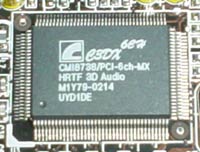
Chaintech set themselves apart from the competition by using a CMedia audio controller instead of the ALC650 AC'97 codec. The CMedia 8738 actually takes the place of the nForce APU which makes very little sense on a nForce2 motherboard since the nForce APU is clearly a much more powerful DSP.
The 7NJS I/O configuration is fairly standard for a high-end desktop motherboard, though we would have like to have seen rear SPDIF out. Included are two PS/2 ports, two serial ports, one parallel port, one game port, one LAN port, two rear USB 2.0 ports, and three 1/8' jacks, which are driven by the onboard sound. No rear FireWire unfortunately, but this board did come with a FireWire riser card.
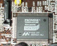
Another intriguing feature this motherboard comes with is Serial ATA support. Serial ATA is powered by Promise's PDC20376 controller (two onboard SATA connectors are available).
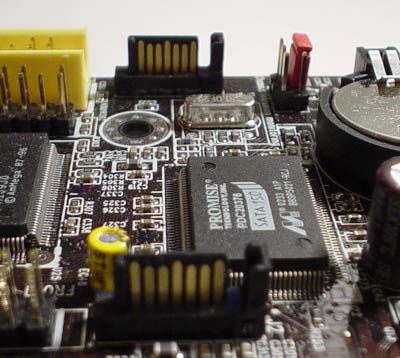
The PDC20376 supports two independent Serial ATA devices as well as IDE RAID 0 (striping) and RAID 1 (mirroring). This is definitely a nice combination of features to have, especially since this is the only nForce2 motherboard that has support for more than four IDE drives through the additional (third) IDE connector located next to the Primary and Secondary IDE connectors. Therefore, users looking to add as many IDE devices to their nForce2 system as possible should look no further than the Chaintech 7NJS.
The MCP-T South Bridge supports USB 2.0, six USB 2.0 ports altogether. There are two rear USB 2.0 ports that you can use if you like, or you can utilize the onboard USB 2.0 headers located towards the bottom of the board near the Primary, Secondary and IDE RAID connectors.
The accessories bundled with this board are quite rich. Chaintech includes:
1. Three 60cm rounded IDE cables.
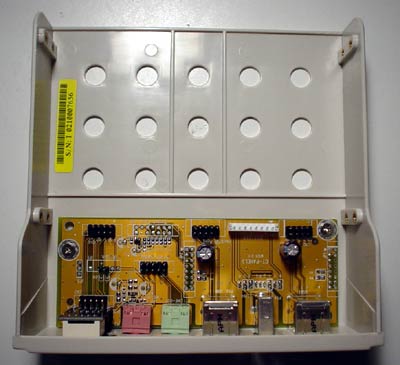
2. A CBOX2 kit with USB and FireWire along with CPU temperature and POST error reporting
3. Two Serial ATA cables.
4. digital audio out port
5. And the rest, which includes the manual and even a golden Chaintech keychain.
All in all, Chaintech really goes all out not just with the onboard features of the 7NJS, but the accessories as well.
Chaintech 7NJS: Board Layout
We didn't have too many complaints with the 7NJS layout, but there certainly were a few.
Chaintech places the ATX (20-pin) connector on the left-hand side of the motherboard. This isn't the best place to put this connector because the thick ATX wires can easily become a nuisance since it'll obstruct the installation/uninstallation of the HSF in addition to any other components that can be modified around that area.
Thankfully, there are four mounting holes around the CPU socket
for those users that desire better cooling solutions than the retail AMD HSF's.
Therefore, cooling fanatics as well as Swiftech and Alpha users should be
happy with the decision to include four mounting holes for cooling.
The Primary, Secondary and RAID IDE connectors are placed in an awkward position
in relation to the AGP slot, just below it in fact. This is a bad layout decision,
as you will likely be forced to maneuver your IDE cables in every which way
to get them to reach an optical drive at the top of your case. The cables
will probably also be hitting the video card on their way up, which yet another
annoyance you don't need.
Another poor layout decision was the placement of the DIMM connectors. The DIMM connectors are nearly touching the video card we used (GeForce4 Ti4600). The main reason we don't like DIMM connectors placed so close to the video card is because you're forced to uninstall your video card if you want to install any additional memory, which is simply a hassle.
There are two USB headers on this motherboard, both of them placed towards the bottom of the board. These headers are placed well only if you don't plan on using the Serial ATA connectors and a USB bracket at the same time. If you do use the Serial ATA connectors, you'll be forced to route the SATA cables through the USB bracket wires, causing all sorts of chaos and clutter.
Chaintech 7NJS: BIOS and Overclocking
Chaintech chose Phoenix Technology's Award BIOS for their nForce2-based 7NJS motherboard. This is the BIOS of choice for nForce2 motherboards so far.

The PC Health section lists a good amount of readings. Here you'll find readings on CPU Vcore, PSU readings (all rails), VDIMM, VAGP, battery voltage, system and CPU temperatures and CPU and system fan speeds. There's also an option for adjusting Shutdown Temperature, which can read as high as 100 C if you want.
The Advanced Chipset Features includes the standard nForce2 options and adjustments. In this section you'll find adjustments for the CPU Interface, CPU multiplier, memory dividers, and various memory timings (including Active to Precharge, Precharge to Active, Active to CMD, and CAS latency). Precharge to Active and Active to CMD timings are adjustable from 1-7T and Active to Precharge is adjustable between 1T and 15T. The Active to Precharge timing ends up being the only setting of the bunch to take advantage of the very flexible DRAM timing options.
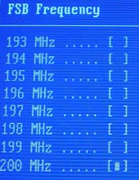
Another option found in the Advanced Chipset Features section is FSB adjustments. The FSB adjustments go as high as 200MHz. The 200MHz FSB limit in the BIOS isn't a big deal when you consider that we weren't able to reliably operate at 200MHz FSB anyway (even with a low CPU multiplier), as you'll see in our overclocking tests shortly.
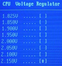
We were very impressed with the available voltage tweaking control in the 7NJS BIOS. For example, Vcore is adjustable all the way up to 2.15V in .025V increments, almost as much as the Epox 8RDA+'s Vcore ceiling. This Vcore should be more than enough for even the most extreme overclockers, and that includes HSF and water cooling overclockers. Thoroughbred-B users should have no issue with a max of 2.15Vcore, as default Thoroughbred-B Vcore is 1.65V. Despite what the 2.15Vcore option might insinuate, you'll "only" get as high as 2.11V if you decide to overvolt that high (which we strongly advise against), as default Thoroughbred-B Vcore fluctuated between 1.60V and 1.61V at idle according to the PC Health readings in the BIOS.
Another very impressive voltage tuning option in the 7NJS BIOS was VDIMM. VDIMM is adjustable all the way up to 3.2V in .01V increments, which is more than even Epox's 8RDA+, which managed no higher than 2.9V (2.92-2.93V actual) in it's BIOS. As read through PC Health, VDIMM fluctuates between 2.53-2.54V when VDIMM is set to 2.6V. Therefore, you'll "only" get 3.13-3.14VDIMM if you decide to overvolt that high. Again, you really don't' need to overvolt much to get a decent memory overclock, so we'd say it's pretty useless to run your memory over 2.8V unless you only plan on using your memory for a short period of time. We'd suggest 2.6V or 2.7V at the most.
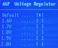
VAGP was yet another voltage that was highly tweakable in the 7NJS BIOS. AGP voltage is adjustable in .1V increments all the way up to 2.0V. Running your AGP at 2.0V is an extremely high voltage for you to be running at, and we strongly suggest against it. Still, it's nice to have for some video card overclockers, even despite the fact that VAPG tweaking doesn't usually aid video overclockers that much.
Even though there's definitely an AGP lock in the 7NJS BIOS, there isn't any visible PCI lock. According to Chaintech though, the 7NJS does indeed lock the PCI bus at 33MHz, there just isn't an option in the BIOS to tinker with it. We have no way of independently verifying this ourselves, so take it for what it's worth.
The Chaintech 7NJS ended up being one of the best FSB overclockers of the bunch, just a tad bit behind the Epox 8RDA+. Here were our FSB overclocking results using the following setup:
|
Front Side Bus Overclocking Testbed |
|
|
Processor:
|
Athlon
XP 2400+
|
|
CPU
Vcore:
|
1.65V
|
|
Cooling:
|
AMD
Retail HSF & Thermal Pad
|
|
Power
Supply:
|
Enermax
300W
|
Using this run-of-the-mill overclocking setup, we were able to hit 190MHz FSB. Not to bad at all, and almost as good as probably the highest overclocking Socket A motherboard on the planet, the Epox 8K5A2+. Thankfully, Chaintech was able to get us their newest BIOS revision to us on time for this review, as the latest BIOS revision added the much needed multiplier adjustments it was lacking with the October 25th BIOS. Therefore, this makes the 7NJS yet another motherboard that is able to adjust the multiplier of a Thoroughbred-B processor without any physical modification whatsoever to the CPU.

These features are necessary to the avid overclocker, which is in part what makes the 7NJS an excellent enthusiast motherboard.
Chaintech 7NJS: Stress Testing
1. Chipset and motherboard stress testing was conducted by running the FSB at 190MHz.
2. Memory stress testing was conducted by running RAM at 333MHz and 400MHz with as many modules populated as possible at the most aggressive timings possible.
Front Side Bus Stress Test Results
At 190MHz FSB, the Chaintech 7NJS had to go through an intensive amount of stress tests just as all the other nForce2 motherboards had to. We began with 24 hours straight of Prime95 torture tests running in the background. In the foreground we had our gaming suite running as well and after that was completed we headed onto general application performance and stability tests with light apps like Word and Excel, and eventually heavier loads like data compression and so on. We also reran a couple more stressful benchmarks like SPECviewperf, XMPEG and Sciencemark. In the end, it was clear that the 7NJS was very reliable at 190MHz FSB, as it didn't fail any of the stress tests we just mentioned.
Memory Stress Test Results
The consistently with which nForce2-based motherboards can operate three memory modules running at 333MHz DDR at the most aggressive possible timings is very impressive. Here were the timings we were able to achieve:
|
Stable
DDR333 Timings |
|
|
Clock
Speed:
|
166MHz
|
|
Timing
Mode:
|
N/A
|
|
CAS
Latency:
|
2
|
|
Bank
Interleave:
|
N/A
|
|
Precharge
to Active:
|
2T
|
|
Active
to Precharge:
|
4T
|
|
Active
to CMD:
|
2T
|
|
Command
Rate:
|
N/A
|
These aggressive timings cannot be matched by anything but an nForce2 motherboard. The Chaintech 7NJS is, not surprisingly, easily able to handle this DRAM settings. Remember, the CPU interface BIOS option is enabled at Aggressive as well, so we squeezed out the best performance we could in this DDR333 situation.
Our final DRAM stress test gauges the ability of the 7NJS to three modules at the best possible timings as high as possible up to 400MHz. Here were the timings we were able to achieve:
|
Stable
DDR400 Timings |
|
|
Clock
Speed:
|
200MHz
|
|
Timing
Mode:
|
N/A
|
|
CAS
Latency:
|
2
|
|
Bank
Interleave:
|
N/A
|
|
Precharge
to Active:
|
2T
|
|
Active
to Precharge:
|
4T
|
|
Active
to CMD:
|
2T
|
|
Command
Rate:
|
N/A
|
Now this is worth noting, mostly because not all the nForce2 motherboards were able to handle three modules running at 400MHz at CAS 2-2-2-4. Chaintech certainly did a fair job with the implementation, so we can be glad of that. Eventually, when the Athlon XP moves to a 400MHz FSB, you'll be able to take advantage of all this bandwidth (assuming you don't overclock).
Memory overclocking turned out to be fairly impressive for the Chaintech 7NJS (at least compared to the nForce2 competition that is). Here were our results.
|
Stable
Memory Overclocking Results |
|||
|
Memory
|
Memory
Clock
|
FSB
|
VDIMM
|
|
Corsair
CAS2.0 DDR400
|
418MHz
|
157MHz
|
2.6V
|
As usual, we ran several memory stress tests and general apps to make sure these DRAM timings and frequencies were stable. We started off by running Prime95 torture tests; a grand total of 24 hours of Prime95 was successfully run at the timings and speeds listed in the above charts. We were also able to run Sciencemark (memory tests only), Super Pi tests and XMPEG encoding successfully while Prime95 was crunching away in the background. All in all, the Chaintech 7NJS proved reliable during all our memory tests.
Chaintech 7NJS: Tech Support and RMA
For your reference, we will repost our support evaluation procedure here:
The way our Tech Support evaluation works is first we anonymously email the manufacturer's tech support address(es), obviously not using our AnandTech mail server to avoid any sort of preferential treatment. Our emails (we can and will send more than one just to make sure we're not getting the staff on an "off" day) all contain fixable problems that we've had with our motherboard. We then give the manufacturer up to 72 hours to respond over business days and will report not only whether they even responded within the time allotted but also if they were successful in fixing our problems. If we do eventually receive a response after the review is published, we will go back and amend the review with the total time it took for the manufacturer to respond to our requests.
The idea here is to encourage manufacturers to improve their technical support as well as provide new criteria to base your motherboard purchasing decisions upon; with motherboards looking more and more alike every day, we have to help separate the boys from the men in as many ways as possible. As usual, we're interested in your feedback on this and other parts of our reviews so please do email us with your comments.
Unfortunately, Chaintech doesn't offer any RMA service to their customers in the U.S., but it varies around the world. Chaintech suggests that you go through the vendor from which you purchased the Chaintech motherboard for an RMA. Clearly this is disappointing when you consider that smaller motherboard makers have been able to provide good, clear RMA policies, and yet Chaintech has none.
However, Chaintech's tech support is different. We very much liked Chaintech's online technical support form, located here. What some may notice first is the well organized and structured nature of tech support form. Chaintech asks for a pretty standard amount of system specifications to better help solve your problems. Here's exactly what Chaintech requires of you:
1. Your personal Information like your first and last name, location, email address and telephone and/or FAX number(s) (phone/FAX number isn't a required field though).
2. The motherboard model number (7NJS in this case), product serial number and the distributor from which you purchased the product (like Newegg or Googlegear for example).
3. The BIOS version, operating system version and all other system specifications like CPU, VGA, memory and any other devices.
4. Description of the precise problem.
After filling out the required fields and pressing the send button, you are taken to another URL where you are told that Chaintech will respond to your email within 5 working (business) days. Indeed, Chaintech did respond within 5 working days, and in just under our 72 hour timeframe. In total, it took Chaintech tech support 69 hours to respond to our email, which is only decent compared to the smaller motherboard makers, but good compared to the top tier motherboard makers. In addition, they were able to solve our "problem" to our satisfaction.
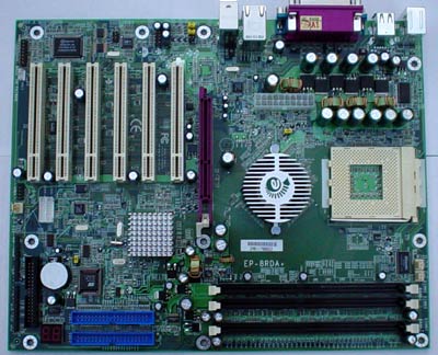
Epox 8RDA+ Rev. 0.3: Basic Features
|
Motherboard Specifications |
|
|
CPU
Interface
|
Socket-462
|
|
Chipset
|
NVIDIA
SPP North Bridge
NVIDIA MCP-T South Bridge |
|
Bus
Speeds
|
100
- 200MHz (in 1MHz increments)
|
|
Core
Voltages Supported
|
up
to 2.20V (in 0.025V increments)
|
|
I/O
Voltages Supported
|
N/A
|
|
DRAM
Voltages Supported
|
up
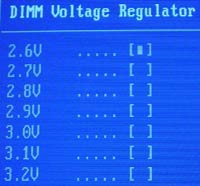
to 2.9V (in 0.13V and 0.14V increments)
|
|
Memory
Slots
|
3
184-pin DDR DIMM Slots
|
|
Expansion
Slots
|
1
AGP 8X Slot
6 PCI Slots |
|
Onboard
ATA RAID
|
N/A
|
|
Onboard
USB 2.0/IEEE-1394
|
USB
2.0 supported through South Bridge
Realtek RTL8801B FireWire PHY (MAC in South Bridge) |
|
Onboard
LAN
|
Realtek
RTL8201BL controller (nForce LAN)
|
|
Onboard
Audio
|
Realtek
ALC650 Controller (nForce2 APU)
|
|
Onboard
Serial ATA
|
N/A
|
|
BIOS
Revision
|
10/28/2002
|
Epox brings a nice combination of features to the table with their first NVIDIA-based motherboard, the Epox 8RDA+ based on the nForce2 SPP North Bridge and MCP-T South Bridge.
The onboard LAN controller is powered by Realtek's RTL8201BL, which is also
found on ABIT and ASUS's nForce2 motherboards. Once again, the 8201BL is the
physical layer for the nForce Ethernet MAC in the MCP-T. EPoX did not include
a second PHY to take advantage of the integrated 3Com MAC so there is only
one 10/100 port on the motherboard.
Like most of the other nForce2 boards, EPoX uses the ALC650 AC'97 codec to take advantage of the nForce APU. Remember that the nForce2 APU only acts as a DSP, final sound quality is still greatly determined by the DAC (Digital to Analog Converter) in the ALC650 AC'97 codec.
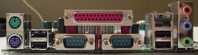
The 8RDA+ I/O configuration is fairly standard for a high-end desktop motherboard. Included are two PS/2 ports, two serial ports, one parallel port, four rear USB 2.0 ports, one LAN port, and three 1/8' jacks, which are driven by the onboard sound. No rear FireWire unfortunately, but there's definitely a couple onboard FireWire headers.
This is yet another nForce2 motherboard that lacks any significant IDE support. Though having Primary and Secondary IDE connectors supporting two channels each is acceptable for even the power user, there will be some that desire more than "just" four drives. Alas, there are no IDE RAID connectors, so four IDE drives are all you're going to get. Interestingly enough Epox bundles two rounded (and blue) IDE cables for you. They measure 60cm in length and should be quite useful in freeing up clutter and air flow inside your computer case.
The MCP-T South Bridge supports USB 2.0, six USB 2.0 ports altogether. There's only one USB 2.0 header that you can use, but the four rear USB 2.0 ports should suffice for most. Epox does include a two-port USB bracket if the rear USB ports aren't enough.
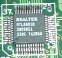
Onboard FireWire support is powered by Realtek's RTL8801B controller, which dictates the data sent to the IEEE 1394a data path integrated into the MCP-T. There are two onboard FireWire headers that you can use as well as a bundled two-port FireWire bracket. In total, this board supports a max of two FireWire ports.
Epox 8RDA+: Board Layout
There weren't too many layout issues to point out with the 8RDA+, but there were a few that we feel are necessary to point out.
On the left-hand side of the motherboard is where we see Epox decided to place the ATX (20-pin) connector. This is not the optimal position to place the connector since the thick ATX wires can easily become a nuisance since it'll obstruct the installation/uninstallation of the HSF in addition to any other components that can be modified around that area. If you're using an especially large HSF, the positioning of the ATX connector is an even bigger inconvenience.
All three onboard fan headers are placed well. The chassis and power fan headers are placed at the very edge of the right-hand portion of the motherboard. This way, fan wires won't have to travel far to their destination. The third fan header however (the CPU fan header) was placed a bit too close to the CPU clamps and DIMM connectors. This makes it somewhat difficult to sneak your fingers in this area to unplug the CPU fan line, but it shouldn't be too much of an issue unless you have large fingers.
We were surprised to see the Primary and Secondary IDE connectors placed in such an awkward position in relation to the AGP slot. Instead of the Primary and Secondary IDE connectors being positioned horizontally on the motherboard, they are placed vertically. Not only that, but the IDE connectors are placed below our installed video card. All in all this is quite a bad layout decision, as you likely be forced to maneuver your IDE cables in every which way to get them to reach an optical drive at the top of your case. The cables will probably also be hitting the video card on their way up.
Another poor layout decision was the placement of the DIMM connectors. The DIMM connectors are nearly touching the video card we used (GeForce4 Ti4600). The main reason we don't like DIMM connectors placed so close to the video card is because you're forced to uninstall your video card if you want to install any additional memory, which is simply a hassle.
Both the USB and FireWire headers are positioned fairly well. In fact, they're placed right next to each other, at the lower half of the mid-section of the motherboard. By positioning these headers in this manner, you're not going to encounter any case clutter, as you the USB and FireWire bracket wires will be taking up the PCI slots you decide to take up, and not any other neighboring PCI slots or other components.
Epox 8RDA+: BIOS and Overclocking
Epox decided to choose Phoenix Technology's Award BIOS for their first nForce2 motherboard. This isn't unusual, especially since all nForce2 motherboards use Award BIOSes.
The PC Health section of the 8RDA+ BIOS includes an average amount of readings. These include system and CPU temperature, fan speeds (chassis, power, and CPU), VAGP, Vcore, VDIMM, PSU readings (all rails), and a battery voltage reading. There are also two other options in this section for adjusting CPU Warning Temperature as well as CPU Shutdown Temperature.
The Advanced Chipset Features section includes the standard amount of options for an nForce2 board, but is quite unconventional compared to the Socket A BIOSes from VIA and SiS motherboards, as all nForce2 BIOSes are. In the 8RDA+ Advanced Chipset Features section, there are adjustments for the CPU multiplier, CPU interface, memory frequency, various memory timings (including Active to Precharge, Precharge to Active, Active to CMD, and CAS latency). Precharge to Active and Active to CMD timings are adjustable from 1-7T and Active to Precharge is adjustable between 1T and 15T. These are definitely the most flexible timings we've ever seen, though only the Active to Precharge timing is able to take advantage of this fact.
The FSB ceiling in the BIOS was surprisingly low, especially for an Epox motherboard. The max available option is 200MHz, which certainly isn't bad, but we would have liked to have seen something higher, as upcoming 200MHz FSB (400MHz effective) Athlon XP Barton processors won't be able to overclock at all using this particular 8RDA+ BIOS. Somehow we doubt Epox will leave out the option for raising the FSB past 200MHz in a future BIOS. 12/04/02 UPDATE: Apparently, there is a very recent 8RDA+ BIOS out that allows up to 211MHz FSB adjustement.
Voltage tweaking potential in the 8RDA+ BIOS is quite good. Vcore is adjustable up to 2.20V in .025V increments. This should be more than enough for even the most extreme overclockers, and that includes HSF and water cooling overclockers. This is especially true of Thoroughbred-B users due to the fact that 2400+ processors and up have a stock Vcore of 1.65V, meaning you can adjust Vcore by a full 0.55V if need be, which is tremendous. Of course, Vcore fluctuates between 1.65 and 1.66V at idle according to the PC Health readings in the BIOS, so you actually have the potential for 2.20V, though we very strongly advise against operating your CPU at this high of a Vcore.
 |
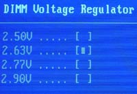 |
Epox has been known to include some impressive VDIMM potential in their performance BIOSes, and this holds true for the most part with the 8RDA+. In 0.13V and 0.14V increments, you're allowed to adjust VDIMM up to 2.9V. VDIMM fluctuates between 2.62 and 2.63V per PC Health, so you can reach an actual 2.9VDIMM. Again, this high of a voltage isn't advisable, as operating your memory at anything over 2.7-2.8V usually isn't a very good idea if you plan on using your RAM for more than a couple months.
As far as we can tell, the Epox 8RDA+ contains just an AGP lock, but no visible PCI lock. We've haven't been able to get confirmation from Epox as to whether this board locks the PCI bus at 33MHz or not, but we'll update this section as soon as we hear back from Epox.
We had absolutely no trouble overclocking the Epox 8RDA+, and in fact, this board ended up achieving the highest stable FSB out of any other nForce2 motherboard tested in our labs. Here were our FSB overclocking results using the following setup:
|
Front Side Bus Overclocking Testbed |
|
|
Processor:
|
Athlon
XP 2400+
|
|
CPU
Vcore:
|
1.65V
|
|
Cooling:
|
AMD
Retail HSF & Thermal Pad
|
|
Power
Supply:
|
Enermax
300W
|
It really isn't in the least surprising that the 8RDA+ was the best overclocker out of our six nForce2 motherboards, as Epox has made much of their reputation on highly overclockable (and reasonably priced) motherboards. So, with the above configuration we were able to hit 194MHz FSB (multiplier set to 8X). On that note, it's worth mentioning that the 8RDA+ is yet another nForce2 motherboard that is able to adjust the Thoroughbred-B's multiplier without having to perform any physical modification to the CPU bridges as was the case with previous generation Athlon XP processors (namely the Thunderbird and Palomino processors).
The 8RDA+ BIOS also comes with a ton of multiplier options ranging from 3X to 24X. These multiplier options should satisfy all users.
Epox 8RDA+: Stress Testing
The abundant array of divider options available in the 8RDA+
BIOS allowed us to test this board in several different areas and configurations,
including:
1. Chipset and motherboard stress testing was conducted by running the FSB at 194MHz.
2. Memory stress testing was conducted by running RAM at 333MHz and 390MHz with as many modules populated as possible at the most aggressive timings possible.
Front Side Bus Stress Test Results
We were pleased (but not surprised) that the Epox 8RDA+ was able to handle such a high FSB with such exceptional stability. At 194MHz FSB, 24 hours straight of Prime95 torture tests was not able to bring the 8RDA+ to its knees. Running Prime95 is a great way to really stress your system, as we have very rarely encountered an issue with a system that was able to pass 24 hours or more of Prime95 torture tests. As Prime95 was running in the background, we reran our gaming suite as well as everyday apps like Word and Excel in addition some data compression here and there. We also managed to rerun SPECviewperf and XMPEG, and added in Sciencemark stress tests (even though we didn't include any Sciencemark numbers in this review). In the end, the 8RDA+ was able to easily pass all these stress tests at 194MHz FSB. Anything over 194MHz FSB did not sufficiently meet our stress testing requirements.
Memory Stress Test Results
Lets see how well the Epox 8RDA+ is able to handle three memory modules installed and running at 333MHz DDR. Here were the timings we were able to achieve:
|
Stable
DDR333 Timings |
|
|
Clock
Speed:
|
166MHz
|
|
Timing
Mode:
|
N/A
|
|
CAS
Latency:
|
2
|
|
Bank
Interleave:
|
N/A
|
|
Precharge
to Active:
|
2T
|
|
Active
to Precharge:
|
4T
|
|
Active
to CMD:
|
2T
|
|
Command
Rate:
|
N/A
|
These are great timings (in fact the A7N8X was able to achieve the exact timings in this exact same scenario). There shouldn't be a single user out there that isn't satisfied with these aggressive timings. We must again note the lower Precharge to Active setting, which other motherboards (not based on the nForce2 chipset) either cannot achieve or simply don't have the option of running at. Also, remember that these timings were achieved with the CPU Interface enabled, which boosts performance a bit.
This final memory test demonstrates the highest frequency the Epox 8RDA+ is able to handle with three memory modules at CAS2/2T/4T/2T. Here were our results:
|
Stable
DDR390 Timings |
|
|
Clock
Speed:
|
190MHz
|
|
Timing
Mode:
|
N/A
|
|
CAS
Latency:
|
2
|
|
Bank
Interleave:
|
N/A
|
|
Precharge
to Active:
|
2T
|
|
Active
to Precharge:
|
4T
|
|
Active
to CMD:
|
2T
|
|
Command
Rate:
|
N/A
|
While we weren't able to hit 400MHz, we did get to 390MHz. With timings like CAS2/2T/4T/2T, we certainly have nothing to complain about. Keep in mind though, if you want the best performance at DDR390 you need to run your FSB at 195MHz, or 390MHz DDR. We were able to reach 194MHz, so that's pretty close to what the 8RDA+'s potential clock frequency ceiling is with all memory banks filled.
The memory overclocking score for the 8RDA+ turned out to be about the average out of all the nForce2 motherboards tested.
|
Stable
Memory Overclocking Results |
|||
|
Memory
|
Memory
Clock
|
FSB
|
VDIMM
|
|
Corsair
CAS2.0 DDR400
|
412MHz
|
165MHz
|
2.63V
|
We had to ensure the various memory timings and frequencies
we were able to operate at were fully stable. Therefore, we conducted 24 hours
of Prime95 torture tests, ran various Super Pi stress tests, and reran various
benchmarks like SPECviewperf 7.0 and XMPEG. All in all, we didn't encounter
any issues with any of the listed memory timings and frequencies we were able
to reach during these stress tests.
SoundStorm Stress Test Results
We ran the same sound tests on the 8RDA+ as we did with all the other nForce2 motherboards tested here today. The following demos were run with SoundStorm sound enabled:
1. Jedi Knight II: Passed
2. Quake 3 Arena: Passed
3. Unreal Tournament 2003: Passed
4. Comanche 4: Passed
5. Serious Sam: Passed
There have been some minor, ongoing issues with NVIDIA's nForce1 APU drivers since the nForce1's introduction last year. Some users have experienced a Blue Screen of Death with nForce sound enabled in certain games. However, the latest nForce2 unified driver package (v 2.00) has seemingly fixed the sound issues that nForce1 users were experiencing. This is backed up by our own test results, which show that SoundStorm is able to smoothly play five of some of the most popular games out there.
Epox 8RDA+: Tech Support and RMA
The way our Tech Support evaluation works is first we anonymously email the manufacturer's tech support address(es), obviously not using our AnandTech mail server to avoid any sort of preferential treatment. Our emails (we can and will send more than one just to make sure we're not getting the staff on an "off" day) all contain fixable problems that we've had with our motherboard. We then give the manufacturer up to 72 hours to respond over business days and will report not only whether they even responded within the time allotted but also if they were successful in fixing our problems. If we do eventually receive a response after the review is published, we will go back and amend the review with the total time it took for the manufacturer to respond to our requests.
The idea here is to encourage manufacturers to improve their technical support as well as provide new criteria to base your motherboard purchasing decisions upon; with motherboards looking more and more alike every day, we have to help separate the boys from the men in as many ways as possible. As usual, we're interested in your feedback on this and other parts of our reviews so please do email us with your comments.
Epox's technical support process, form, etc. hasn't changed since the last time we took a look at an Epox motherboard.
Epox's technical support form is quite long, but well rounded nonetheless. Epox asks you to fill out, among other things, your personal info, email address, motherboard model, serial number, vendor from whom you purchased the Epox product from and your system specifications (BIOS version, video card, CPU, etc.). You then have to briefly write out exactly what your issue(s) are and you're done. All in all we like this type of technical support procedure, it's well organized.
Epox's technical support response time was just as good this time around, in fact it was a bit better. We were able to get a reply from Epox tech support within 34 hours instead of 35 hours like the last time around. Epox was also able to answer our "problem" sufficiently enough. Epox's tech support response pattern so far has been very impressive, let's hope they're able to keep it up, as they need to differentiate themselves from top tier motherboard makers as much as they can.
Epox very clearly lists their RMA policy and procedure on their web site. For some odd reason, some of the larger motherboard makers do not feel that it is necessary to clearly and explicitly list exactly what their RMA procedures entail on their web site. Thankfully Epox doesn't follow suit.
For your reference, here is Epox's RMA policy in its entirety:
|
This is a fairly straight forward RMA procedure. Compared to
online hardware vendors like Newegg, this RMA process really isn't too different.
All in all, Epox's technical support and RMA policy still seem to be top-notch since the last time we took a look at it, and it's certainly better than even several top-tier motherboard makers.
Leadtek K7NCR18D Rev. B: Basic Features
|
Motherboard Specifications |
|
|
CPU
Interface
|
Socket-462
|
|
Chipset
|
NVIDIA
SPP North Bridge
NVIDIA MCP-T South Bridge |
|
Bus
Speeds
|
100
- 200MHz (in 1MHz increments)
|
|
Core
Voltages Supported
|
up
to 2.00V (in 0.025V increments)
|
|
I/O
Voltages Supported
|
N/A
|
|
DRAM
Voltages Supported
|
up
to 2.7V (in 0.1V increments)
|
|
Memory
Slots
|
3
184-pin DDR DIMM Slots
|
|
Expansion
Slots
|
1
AGP 8X Slot
4 PCI Slots |
|
Onboard
ATA RAID
|
N/A
|
|
Onboard
USB 2.0/IEEE-1394
|
USB
2.0 supported through South Bridge
Realtek RTL8801B FireWire PHY (MAC in South Bridge) |
|
Onboard
LAN
|
Realtek
RTL8201BL controller (nForce LAN)
|
|
Onboard
Audio
|
Realtek
ALC650 Controller (nForce2 APU)
|
|
Onboard
Serial ATA
|
N/A
|
|
BIOS
Revision
|
11/06/2002
|
Leadtek is known as a video card manufacturer more than anything else, so seeing a Leadtek-powered motherboard review is quite rare indeed. However, today we take a look at Leadtek's latest motherboard, the K7NCR18D. Based on the nForce2 SPP and MCP-T, lets first take a look at what features this board has to offer.
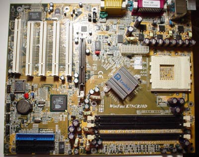
The K7NCR18D uses the same RTL8201BL PHY that we've seen on other motherboards. Even though the MCP-T South Bridge has support for a dual onboard LAN ports, Leadtek decided to leave out the second (3Com) port and PHY to minimize costs.
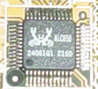
You'll also find a Realtek ALC650 AC'97 codec onboard the K7NCR18D, which does all the sound processing. Remember that the nForce2 APU only acts as a DSP, final sound quality is still greatly determined by the DAC (Digital to Analog Converter) in the ALC650 AC'97 codec.
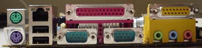
There's nothing special to report about the K7NCR18D's I/O configuration. Among the I/O ports are two PS/2 ports, one LAN port, two rear USB 2.0 ports, one parallel port, two serial ports, nd three 1/8' jacks, which are driven by the onboard sound. Though not too shabby, we would have liked to have seen a couple extra USB ports in addition to a SPDIF out possibly.
The Leadtek K7NCR18D is yet another nForce2 motherboard that lacks IDE RAID or any other form of additional IDE support besides the standard Primary and Secondary IDE connectors. With support for up to two channels each, the K7NCR18D is capable of supporting no more than four IDE drives total. So, if you can deal with a max of two hard drives and two optical drives (or a similar combination thereof), then you shouldn't have anything to worry about with this particular motherboard.
The MCP-T South Bridge supports the latest serial standard, USB 2.0. In fact, the MCP-T supports six USB 2.0 ports altogether; two rear USB 2.0 ports and two onboard USB 2.0 headers that support an additional four USB 2.0 ports if the rear ports aren't enough to meet your needs. Unfortunately, Leadtek doesn't bundle a USB 2.0-compliant bracket with their K7NCR18D, which is a notable setback.
Leadtek K7NCR18D: Board Layout
There were a few glaring layout issues that we feel are worth pointing out.
The Leadtek K7NCR18D places the ATX (20-pin) connector on the left-hand side of the motherboard below the left-hand corner of the CPU socket. This simply isn't the best place to position the ATX connector layout-wise due to the fact that thick ATX wires can obstruct the installation/uninstallation of the HSF in addition to any other components that might be modified around that area.
There are a total of two onboard fan headers on the included with the MSI K7N2-L. One is the CPU fan header, which is spoken for, and the other is the North Bridge fan header, an RPM reading of which you will find in the BIOS. Of course, you'll have to mod the motherboard with a North Bridge HSF that fits if you want to use this onboard header, though you can always use it for a case fan.
For those users looking to mount their 4-hole heatsinks, have no fear, Leadtek has kindly included four mounting holes around the CPU socket for your installing pleasure. Therefore, you should be able to use Alpha PAL and Swiftech SLK HSF's without issue.
Annoyingly enough, Leadtek places the Primary and Secondary IDE connectors in a similarly awkward position as the K7N2-L and 8RDA+'s location. The Primary and Secondary IDE connectors are located so low on the K7NCR18D that they almost touch the very bottom of the board. Again, we would find it hard to believe if IDE cables running from these connectors would even be able to reach the upper two drive bays of a large sized ATX case. Assuming you're using a long video card, your IDE cables might also get tangled up with your video card. All in all, this isn't too convenient of a location if you plan on keeping your case nice and clean.
Thankfully, Leadtek positioned the DIMM connectors well enough away from the video card to prevent any installation issues. The GeForce4 we used had plenty of room between itself and the DIMM connectors. It's nice to see this space between DIMM connector and video PCB as you aren't forced to uninstall your video card if you need to add memory to your system. An example (which we previously just mentioned with the MSI K7N2-L) of a common scenario where you might need to add memory to your system while your video card is installed is when you're upgrading your system for the first time in quite a while, and you decide to add a large stick of high-speed memory to boost application performance.
There are two USB 2.0 headers located on the K7NCR18D, where you can plug in up to four USB 2.0 ports. We have always liked this type of header location because the bracket wires won't get engulfed between other cables and wires that may be connected to the motherboard. Therefore, the location of the USB headers decreases clutter and increases air flow, which is exactly what you want.
Leadtek K7NCR18D: BIOS and Overclocking
Leadtek decided to go for Phoenix Technology's Award BIOS with their K7NCR18D series of nForce2 motherboards.
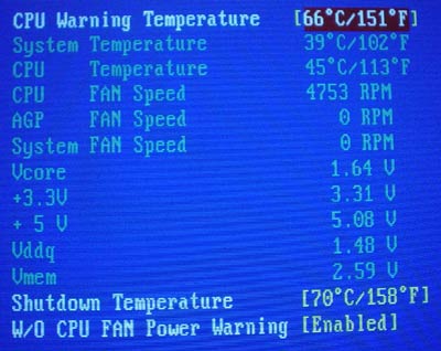
The BIOS hardware monitor, dubbed PC Health, includes a nice combination of readings and overheating protection options. As far as the readings are concerned, they range from system and CPU temperature, three fan speed readings (CPU, AGP and system), Vcore, PSU readings (3V and 5V rail only), VAGP and VDIMM. There are also three different options for CPU overheating protection; CPU Warning Temperature, Shutdown Temperature and W/O CPU Fan Power Warning. All in all, this is a nice combination of BIOS features to have, especially if you ever run into thermal issues with our Athlon XP.

The K7NCR18D contains an Advanced Chipset Features section with various options for adjusting any of a number of things. Here you're allowed to adjust the CPU interface, memory dividers, and various memory timings (including Active to Precharge, Precharge to Active, Active to CMD, and CAS latency). As with all the other nForce2 BIOSes, the Precharge to Active and Active to CMD timings are adjustable from 1-7T, and Active to Precharge is adjustable from 1-15T. No other non-nForce motherboards contain such flexible timings.
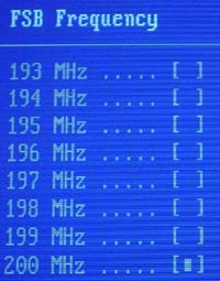
Another option within the Advanced Chipset Features section is an adjustment for FSB overclocking up to 200MHz in 1MHz increments. This doesn't bode well for overclockers planning on upgrading to 400MHz FSB Athlon XP Barton CPU's next year, as this leaves zero room for overclocking. However, we can't rule out the possibility that Leadtek will release a BIOS that contains higher FSB adjustments. Still, a FSB ceiling of 200MHz isn't bad by any means for the vast majority of users (and especially those that don't overclock, which is by far the majority of users). 12/04/02 UPDATE: Leadtek has a slightly newer BIOS out that allows FSB adjustments up to 211MHz, while everything else is kept the same.
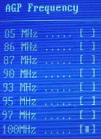
There's one section of the K7NCR18D BIOS that makes this board "stand out" somewhat, and it's called the X-BIOS II section. Here, you have access to a fair amount of voltage tweaking options, including AGP frequency adjustments up to 100MHz in 1MHz increments, VAGP and Vcore.
Vcore flexibility is much better than some of the other nForce2 boards tested here today. In .025V increments you can adjust Vcore up to 2.00V. Luckily for some, this voltage can be attained in reality, as the default Vcore as read by the PC Health section of the BIOS reads a steady 1.64V, meaning just about 2.00V is possible. So, Palomino and Thoroughbred overclockers of almost all walks should be quite pleased with this setting. Unfortunately, Leadtek wasn't equally kind enough to include any multiplier adjustments in their BIOS, meaning your CPU will likely become the bottleneck before the FSB does, which isn't ideal whatsoever. Remember, we used an 8X multiplier for all nForce2 FSB overclocking.
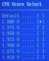
For some odd reason, there doesn't seem to be any VDIMM adjustments available anywhere in this BIOS. While not a huge loss for a majority of users, it's definitely a loss to the tweakers and (some) overclockers out there. Due to the fact that we couldn't adjust VDIMM
VAGP is also adjustable in the X-BIOS II menu. You can adjust the VAGP in 0.1V increments up to 1.7V from the default 1.5V. If you were to set VAGP to 1.7V, you'd get more like 1.68V according to the BIOS hardware monitor, so video card overclockers should be pleased, even though raising VAGP usually isn't necessary to begin with. AGP frequency is also adjustable in X-BIOS II. In 1MHz increments, you can adjust AGP frequency up to 100MHz. Yes, this is clearly overkill, but nice to have if you're really into video overclocking. Just be careful you don't run your AGP frequency too far out of spec.
While the Leadtek K7NCR18D has an AGP lock in its BIOS, we were unable to determine if this board enabled PCI locking. We asked Leadtek about this, and so far we haven't received a clear response. Once we find out what the deal is with PCI locking, we'll update this section. 12/04/02 UPDATE: Leadtek has finally gotten back to us and, according to them, their K7NCR18D does not include a PCI bus lock at 33MHz, and therefore the PCI bus will be overclocked at certain overclocked FSB speeds.
The Leadtek K7NCR18D ended up being the poorest FSB overclockers of all the nForce2 boards, but that can simply be attributed to the fact that there are zero multiplier options available in the BIOS of this board. Here were our FSB overclocking results using the following setup:
|
Front Side Bus Overclocking Testbed |
|
|
Processor:
|
Athlon
XP 2400+
|
|
CPU
Vcore:
|
1.65V
|
|
Cooling:
|
AMD
Retail HSF & Thermal Pad
|
|
Power
Supply:
|
Enermax
300W
|
As just mentioned, the K7NCR18D BIOS does not include any multiplier adjustments. This fact makes it impossible to independently verify what the true maximum FSB the K7NCR18D is able to operate at. Since all the other nForce2 motherboards reached overclocked FSB numbers into the mid 180's, we used an Athlon XP 2600+ (333MHz FSB) CPU for our overclocking tests to see how much further above 166MHz FSB the K7NCR18D could go. With stock retail cooling, not too far obviously. We were able to get to 176MHz max, though this was using a 12.5 multiplier. We're sure some users would like Leadtek to release a new BIOS with multiplier adjustments in the future, as this would definitely boost FSB overclocking past 176MHz.
Leadtek K7NCR18D: Stress Testing
There were plenty of memory divider options available in the BIOS for us to test this board in several different areas and configurations, including:
1. Chipset and motherboard stress testing was conducted by running the FSB at 176MHz.
2. Memory stress testing was conducted by running RAM at 333MHz and 376MHz with as many modules populated as possible at the most aggressive timings possible.
Front Side Bus Stress Test Results
Our FSB stress tests went without issue at 176MHz FSB. The K7NCR18D had no trouble going through 24 hours of Prime95 torture tests without a single failure. As usual, we had Unreal Tournament, Quake 3 Arena and Jedi Knight II demos running one after another with Prime95 crunching in the background. In addition, we performed some general work like data compression in addition to light Word and Excel apps. SPECviewperf and XMPEG were also run to further stress test the K7NCR18D to see if it would crack. Despite it all, the Leadtek K7NCR18D was as solid as a rock in the limited stress testing we conducted at 176MHz FSB. We wonder how much higher the K7NCR18D would have gone had there been CPU multiplier options in the BIOS.
Memory Stress Test Results
This first memory stress test tests how the Leadtek K7NCR18D is able to handle DDR333 speeds at aggressive timings with all memory banks occupied. Here were our results:
|
Stable
DDR333 Timings |
|
|
Clock
Speed:
|
166MHz
|
|
Timing
Mode:
|
N/A
|
|
CAS
Latency:
|
2
|
|
Bank
Interleave:
|
N/A
|
|
Precharge
to Active:
|
2T
|
|
Active
to Precharge:
|
4T
|
|
Active
to CMD:
|
2T
|
|
Command
Rate:
|
N/A
|
There are very impressive timings for three memory modules running at 333MHz. No surprise though, as all the nForce2 boards we've tested up to this point have been able to operate with these exact same memory settings.
The following chart lists the highest frequency we were able to reach at the following memory timings with all memory banks occupied. Here were our results:
|
Stable
DDR376 Timings |
|
|
Clock
Speed:
|
188MHz
|
|
Timing
Mode:
|
N/A
|
|
CAS
Latency:
|
2
|
|
Bank
Interleave:
|
N/A
|
|
Precharge
to Active:
|
2T
|
|
Active
to Precharge:
|
4T
|
|
Active
to CMD:
|
2T
|
|
Command
Rate:
|
N/A
|
The highest we could get with the K7NCR18D was 376MHz with three DIMMs operating at these timings. This frequency is certainly noticeably below the average for an nForce2 board, but still decent nonetheless.
Our memory overclocking results for the K7NCR18D were similarly unspectacular. Here were our results:
|
Stable
Memory Overclocking Results |
|||
|
Memory
|
Memory
Clock
|
FSB
|
VDIMM
|
|
Corsair
CAS2.0 DDR400
|
408MHz
|
163MHz
|
2.56V
|
We ran our usual set of memory "stressmarks" to ensure that our memory timings and memory frequencies were reliable enough to mimic prolonged operation. Therefore, we first started out by conducting 24 hours straight of Prime95 torture tests. Then, we moved on to Super Pi stress tests in addition to rerunning benchmarks like SPECviewperf 7.0 and XMPEG. All in all, the K7NCR18D proved to be quite reliable at the above listed memory timings and frequencies for us to be able to proclaim the Leadtek K7NCR18D stable at these settings.
SoundStorm Stress Test Results
We ran the same sound tests on the K7NCR18D as we did with all the other nForce2 motherboards tested here today. The following demos were each run three times with SoundStorm enabled:
1. Jedi Knight II: Passed
2. Quake 3 Arena: Passed
3. Unreal Tournament 2003: Passed
4. Comanche 4: Passed
5. Serious Sam: Passed
As we previously mentioned, there have been some minor, ongoing issues with NVIDIA's nForce1 APU drivers since the nForce1's introduction last year. Some users have experienced a Blue Screen of Death with nForce sound enabled in games like Unreal Tournament. However, the latest nForce2 unified driver package (v 2.00) has seemingly fixed the sound issues that nForce1 users were experiencing. This is backed up by our own stress test results, which show that SoundStorm is able to smoothly play five of some of the most popular games out there, including Unreal Tournament (which experienced the previously mentioned sound issues before the 2.00 drivers were released).
Leadtek K7NCR18D: Tech Support and RMA
For your reference, we will repost our tech support evaluation procedure here:
The way our Tech Support evaluation works is first we anonymously email the manufacturer's tech support address(es), obviously not using our AnandTech mail server to avoid any sort of preferential treatment. Our emails (we can and will send more than one just to make sure we're not getting the staff on an "off" day) all contain fixable problems that we've had with our motherboard. We then give the manufacturer up to 72 hours to respond over business days and will report not only whether they even responded within the time allotted but also if they were successful in fixing our problems. If we do eventually receive a response after the review is published, we will go back and amend the review with the total time it took for the manufacturer to respond to our requests.The idea here is to encourage manufacturers to improve their technical support as well as provide new criteria to base your motherboard purchasing decisions upon; with motherboards looking more and more alike every day, we have to help separate the boys from the men in as many ways as possible. As usual, we're interested in your feedback on this and other parts of our reviews so please do email us with your comments.
Leadtek’s technical support process doesn’t seem to be too bad at all. There are two phone numbers you can reach Leadtek tech support at in the U.S., and they are 1-888-Leadtek or 510-490-8076. Leadtek’s phone tech support hours are 9:00am to 6:00pm, which is just a bit better than the standard for motherboard makers these days. Of course, there’s also the tech support email address you can reach Leadtek at, which is as follows: [email protected].
Leadtek's tech support form is concise but not lacking in usefulness. Their tech support form asks you to fill out a number of things, including:
1. Personal information, which includes your full name, location (full address), your current employer (company name), email address and phone number.
2. The Leadtek product you are having difficulties operating.
3. The vendor you purchased the product from and the date.
4. Your exact system specifications, including motherboard, CPU, memory, chipset, BIOS, Operating System, DirectX version in use, video card BIOS and model, IRQ usage, and any peripherals.
5. And lastly, the specific problem that is bothering you.
End users shouldn’t have any trouble filling out all this information, though some of the system specifications they ask for are a bit odd (like video card BIOS rev. and IRQ usage). Still, this organized and concise technical support form should satisfy the majority of users.
Leadtek's tech support was unable to respond within the 72 hour timeframe we've set up. This is a bit dissapointing, as the smaller motherboard makers usually have good, solid tech support response time. We'll see what happens the next time we take a look at Leadtek's tech support response time.
Leadtek’s RMA procedure works much in the same way their tech support form works. In fact, you must work through and send your RMA request through the tech support form if you are in North America. Leadtek tells us that they’ll assign you an RMA number and send you a brand new model once the details are ironed out between you and your tech support representative. Leadtek even offers to pretest your replacement board (under certain circumstances) before it's shipped out so as to ensure functionality. Doesn’t seem like too bad of a deal overall.
However, what Leadtek needs to improve on is the availability of RMA information on their web site. They don’t have an RMA policy or even some type of RMA FAQ explaining how their return and defective parts policies work. If I weren’t working for AnandTech, I would have a hell of a time figuring out what Leadtek’s RMA policy entails, as it’s not conveniently available on their web site.
Another positive aspect of Leadtek's motherboard customer service is their contact information. If you visit this link you'll find information on where to contact Leadtek in the U.S.A., Taipei, Shanghai and Europe. Leadtek lists a phone number, fax number, exact location and address in addition to a URL to visit for more information pertaining to each of the four regions of the world listed.
MSI K7N2-L: Basic Features
|
Motherboard Specifications |
|
|
CPU
Interface
|
Socket-462
|
|
Chipset
|
NVIDIA
SPP North Bridge
NVIDIA MCP-T South Bridge |
|
Bus
Speeds
|
100
- 200MHz (in 1MHz increments)
|
|
Core
Voltages Supported
|
up
to 1.80V (in 0.025V increments)
|
|
I/O
Voltages Supported
|
N/A
|
|
DRAM
Voltages Supported
|
up
to 2.7V (in 0.1V increments)
|
|
Memory
Slots
|
3
184-pin DDR DIMM Slots
|
|
Expansion
Slots
|
1
AGP 8X Slot
5 PCI Slots |
|
Onboard
ATA RAID
|
N/A
|
|
Onboard
USB 2.0/IEEE-1394
|
USB
2.0 supported through South Bridge
No FireWire |
|
Onboard
LAN
|
Realtek
RTL8201BL controller (nForce LAN)
|
|
Onboard
Audio
|
Realtek
ALC650 Controller (nForce2 APU)
|
|
Onboard
Serial ATA
|
N/A
|
|
BIOS
Revision
|
W6570SP
V3.0B4 11/22/02
|
The MSI K7N2-L will be the only nForce2 SPP motherboard MSI produces, as MSI has decided to concentrate a bit more on the nForce2 IGP side of things this time around. Therefore, MSI is going to have two IGP products ready come mid-January, which is when they expect mass production.
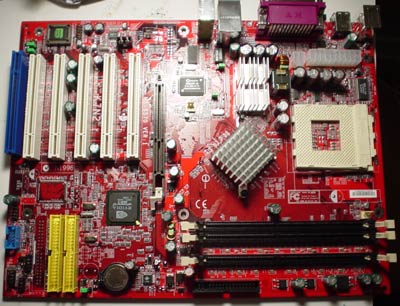
The first of the two IGP products is dubbed the K7N2G-L, which comes with nForce LAN, nForce sound and integrated graphics for an estimated MSRP of $118. The K7N2G-ILSR comes with nForce LAN, nForce sound, FireWire, Serial ATA RAID and integrated graphics for an MSRP of $138. MSI says these prices aren't definite yet, but if the final price is even remotely close to this, they'll be quite the bargain.
Onboard LAN is included with the K7N2-L, and is powered by the PH163112 controller. This controller accesses one of the two MAC's integrated into the MCP-T; the nForce MAC in this case. Once again we see that only one of the two integrated MACs are taken advantage of.
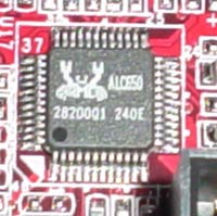
As usual, the Realtek ALC650 acts as the controller chip for sound processing on the K7N2-L. Remember that the nForce2 APU only acts as a DSP, final sound quality is still greatly determined by the DAC (Digital to Analog Converter) in the ALC650 AC'97 codec.
The K7N2-L I/O configuration is like most of the other nForce2 boards. Included are two PS/2 ports, one serial port, one parallel port, four rear USB 2.0 ports, one LAN port, and three 1/8' jacks, which are driven by the onboard sound. All in all, quite acceptable for most users.
This motherboard, like most of the other nForce2 boards, lacks more than just Primary/Secondary IDE support. The Primary and Secondary IDE connectors support two channels each, or up to four IDE drives total. This isn't enough for some people, although most users should be satisfied.
The MCP-T South Bridge supports USB 2.0, six USB 2.0 ports altogether. There's a single USB 2.0 header located towards the bottom of the motherboard, just below the last IDE connector if you feel the four rear USB 2.0 ports aren't acceptable. MSI is good enough to bundle a two-port USB 2.0 bracket, which is slowly starting to become a standard accessory in high-end desktop motherboards nowadays. This is becoming standard even with value motherboards.
MSI K7N2-L: Board Layout
The MSI K7N2-L didn't have too many major layout issues, though there were a few that caught our attention and that should be noted.
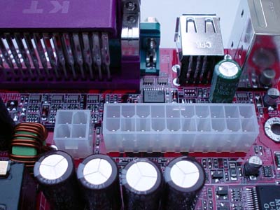
The ATX (20-pin) connector is located on the left-hand side of the motherboard next to the I/O ports. We've always said that this isn't the best place for the ATX connector to be because the thick ATX wires can obstruct the installation/uninstallation of the HSF in addition to any other components that might be modified around that area. On that note, we should say that we were disappointed that the capacitors around the CPU socket were a bit too close for certain types of large heatsinks. Since the mounting holes are missing in the first place, installing the higher quality MCX and PAL heatsinks won't be possible anyway. We're not sure why MSI continues to leave out the four mounting holes.
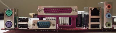
There are a total of two onboard fan headers on the included with the MSI K7N2-L. One is the CPU fan header, which is spoken for, and the other is the North Bridge fan header, an RPM reading of which you will find in the BIOS. Of course, you'll have to mod the motherboard with a North Bridge HSF that fits if you want to use this onboard header, though you can always use it for a case fan instead.
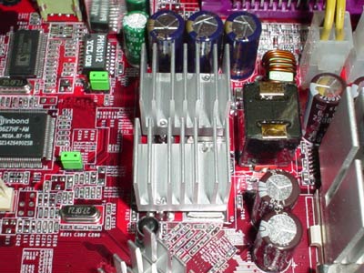
Lately, we've seen MSI add on passive cooling to their voltage regulators, as you can see in the picture above.
We also see a blue PCI slot located at the very bottom of the motherboard, which resembles ASUS's "Blue Magic" slot technology. Apparently, this is an ACR slot for future SoundStorm expansion. MSI wasn't able to elaborate any further than that, but we'll update this info if we do get more information from MSI.
Like the Epox 8RDA+, the Primary and Secondary IDE connectors are placed in a very awkward position in relation to the AGP slot. However, the IDE connector's location on the K7N2-L is even worse than the 8RDA+'s location. The K7N2-L places the Primary and Secondary IDE connectors even lower on the motherboard, close to the USB header. We would find it hard to believe if IDE cables running from these connectors would even be able to reach the upper two drive bays of a large sized ATX case. This is, of course, unacceptable, especially for power users that are looking for a quality computer case (which are usually quite large compared to your Joe Average OEM computer cases from Dell). In addition to all of this, the IDE cables will probably be hitting your video card, though that's assuming your video card is as long as ours.
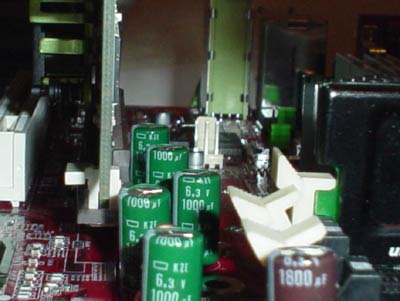
Luckily enough, the DIMM connectors are placed nicely. The GeForce4 Ti4600 we used had plenty of room between itself and the DIMM connectors. This is nice to see as you aren't forced to uninstall your video card if you need to add memory to your system. An example of a common scenario where you might need to add memory to your system while your video card is installed is when you're upgrading your system for the first time in quite a while, and you decide to add a large stick of high-speed memory to boost application performance.
There's just one USB 2.0 header, and it's located at the bottom of the board, colored in blue. This is a good place to position the USB 2.0 header, as the wires from a USB 2.0 bracket won't collide with any other PCI cards you may or may not decide to install in your motherboard, in addition to any other components that may stick out. This location also helps reduce clutter of course, which is a bonus for those that upgrade frequently.
MSI K7N2-L: BIOS and Overclocking
MSI decided to use Phoenix Technology's Award BIOS for their nForce2 motherboard, and this certainly isn't bucking the trend, as all nForce2 motherboards use an Award BIOS.
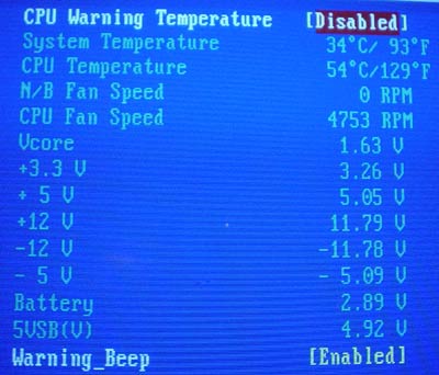
BIOS hardware monitoring can be found in the PC Health section. In general, we see a fair amount of readings, ranging from system and CPU temperature, North Bridge and CPU fan speed, Vcore, PSU readings (all rails), battery voltage, and options for enabling or disabling CPU Warning Temperature and Warning Beep. All in all this is a very basic PC Health section. Worthy of note is the available North Bridge fan speed reading that is present, despite the fact that the North Bridge is passively cooled. Therefore, you should have no trouble replacing the passive North Bridge heatsink for an active cooling solution in the future.
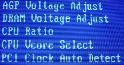
The Advanced Chipset Features section contains options for adjusting a large array of things. In this section, you're allowed to adjust the CPU interface, memory dividers and various memory timings (including Active to Precharge, Precharge to Active, Active to CMD, and CAS latency). As with most of the other nForce2 BIOSes, the Precharge to Active and Active to CMD timings are adjustable from 1-7T, and Active to Precharge is adjustable from 1-15T. Though the Active to Precharge timing was the only timing able to take advantage of these abundant options, it's nice to have nonetheless.
The FSB options top out at 200MHz (1MHz increments) in the K7N2-L BIOS unfortunately. We hope to see an updated BIOS with higher FSB adjustments in the future simply due to the fact that some overclockers will want to run their 400MHz FSB Athlon XP Bartons higher than their stock FSB setting. For example, a 250MHz setting would be nice to see in a future K7N2-L BIOS update.
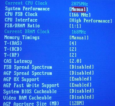
Voltage tweaking is made possible by the "Frequency/Voltage Control" section. In this section you'll find options for adjusting AGP up to 120MHz in 1MHz increments, VAGP, VDIMM, CPU multiplier, Vcore, and what appears to be a PCI lock control option (which we're not sure about yet).
There will be many users disappointed with the lack of flexible Vcore adjustment in this BIOS version. The max attainable Vcore via the K7N2-L BIOS is 1.80V, and what's even worse is that actual Thoroughbred-B Vcore fluctuates between 1.61-1.62V (instead of 1.65V). This means that consumers that planning on using their Palomino processors in the K7N2-L (and plan on doing some overclocking) will have to stay very near to the 1.75V spec of those CPU's. However, for Thoroughbred-A/B users, the actual attainable Vcore of 1.77V or so should be enough, though there will undoubtedly be some who won't be satisfied with 1.77V.
VDIMM adjustments weren't all that impressive either. You can "only" adjust VDIMM as high as 2.7V. Though having the potential to go any higher than 2.7V probably won't yield you a better memory overclock, it's still nice to have for some overclockers. We should remind you that running much higher than 2.8VDIMM is bad for the longevity of your memory.
We still haven't been able to get confirmation from MSI as to whether the K7N2-L locks the PCI bus at 33MHz. There is an AGP lock at 66MHz for this board (as with all nForce2 boards). We'll immediately update you with more information as we receive it from MSI. 12/04/02 UPDATE: MSI sends word that the K7N2-L indeed does not have a PCI bus lock at 33MHz, meaning you will overclock your PCI bus to a certain level at a certain overclocked FSB speed.
The MSI K7N2-L ended up performing in the middle of the pack as far as FSB overclocking was concerned. Here were our FSB overclocking results using the following setup:
|
Front Side Bus Overclocking Testbed |
|
|
Processor:
|
Athlon
XP 2400+
|
|
CPU
Vcore:
|
1.65V
|
|
Cooling:
|
AMD
Retail HSF & Thermal Pad
|
|
Power
Supply:
|
Enermax
300W
|
With this very common overclocking setup, we were able to hit 186MHz FSB, which was exactly what the ABIT NF7-S was able to achieve and 1MHz higher than the ASUS A7N8X. It's obvious that a good chunk of the nForce2 boards tested here today are limited to somewhere in the mid-180MHz FSB range, while only Epox's 8RDA+ and Chaintech's 7NJS are able to reliably operate at anything above that FSB range (190MHz and 194MHz respectively).
MSI includes some fairly limited multiplier options, ranging from just 7X to 13X in 0.5X increments. This will be a disadvantage to some power users, but should satisfy most overall. For our FSB tests, we lowered the multiplier to 8X. The MSI K7N2-L is yet another motherboard that is able to unlock factory locked Thoroughbred-B processors. Therefore, we were able to unlock our Athlon XP 2400+ with ease on the K7N2-L.
MSI K7N2-L: Stress Testing
There were plenty of memory divider options available in the BIOS for us to test this board in several different areas and configurations, including:
1. Chipset and motherboard stress testing was conducted by running the FSB at 186MHz.
2. Memory stress testing was conducted by running RAM at 333MHz and 392MHz with as many modules populated as possible at the most aggressive timings possible.
Front Side Bus Stress Test Results
Our FSB stress tests went very well at 186MHz FSB. At this speed, we were able to run 24 hours of Prime95 torture tests without error. Even more impressive was the fact that the K7N2-L was able to complete Prime95 while we reran our gaming suite (Unreal Tournament, Quake 3 Arena, Jedi Knight II) in addition to data compression and Word and Excel apps. We were able to find time to run SPECviewperf and XMPEG to further stress the K7N2-L. In the end, our best efforts to bring the K7N2-L to its knees at 186MHz FSB proved fruitless.
Memory Stress Test Results
Our initial memory stress test will gauge how well this nForce2 motherboard lives up to its memory compatibility claims. We'll do this by installing three Corsair XMS memory modules running at 333MHz DDR. Here were the timings we were able to achieve:
|
Stable
DDR333 Timings |
|
|
Clock
Speed:
|
166MHz
|
|
Timing
Mode:
|
N/A
|
|
CAS
Latency:
|
2
|
|
Bank
Interleave:
|
N/A
|
|
Precharge
to Active:
|
2T
|
|
Active
to Precharge:
|
4T
|
|
Active
to CMD:
|
2T
|
|
Command
Rate:
|
N/A
|
These are exactly the type of timings we love to see at DDR333 speeds. Users that want to tweak their system to the max but don't want to overclock or anything else fancy like that will be delighted to learn that installing three memory modules running at 333MHz at these timings is ridiculously easy for the K7N2-L, not to mention all the nForce2 motherboards.
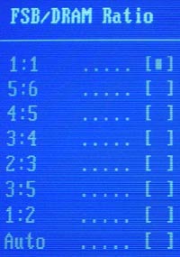
The following chart lists the highest frequency we were able to reach at the same memory timings listed above, with all memory banks occupied. Here were our results:
|
Stable
DDR392 Timings |
|
|
Clock
Speed:
|
196MHz
|
|
Timing
Mode:
|
N/A
|
|
CAS
Latency:
|
2
|
|
Bank
Interleave:
|
N/A
|
|
Precharge
to Active:
|
2T
|
|
Active
to Precharge:
|
4T
|
|
Active
to CMD:
|
2T
|
|
Command
Rate:
|
N/A
|
While 400MHz wasn't possible, 392MHz certainly was. We certainly can't complain about the results, as these would be stellar timings for any other non-nForce2 motherboard. Remember, to take advantage of these high memory speeds, you must run your FSB in sync. In other words, when running at DDR392, make sure you FSB is set to 196MHz in the BIOS (assuming you want to overclock of course). Though, since the K7N2-L was able to reach no higher than 186MHz FSB, you should run your memory at 372MHz DDR for the best possible performance.
Our memory overclocking results for the MSI K7N2-L was nothing to get excited about compared to the other nForce2 motherboards. Here were our results:
|
Stable
Memory Overclocking Results |
|||
|
Memory
|
Memory
Clock
|
FSB
|
VDIMM
|
|
Corsair
CAS2.0 DDR400
|
410MHz
|
164MHz
|
2.6V
|
As usual, we made sure to thoroughly test each memory timing and memory frequency we were able to reach with the K7N2-L. Of course, this meant conducting 24 hours of Prime95 torture tests, which were passed successfully in all scenarios. We also decided to run some Super Pi stress tests in addition to rerunning benchmarks like SPECviewperf 7.0 and XMPEG. The end result of all our stress tests was positive, we didn't encounter any instability (that we could notice at least), and in general the K7N2-L operated just as well as it did previously at stock clock speeds and memory settings.
SoundStorm Stress Test Results
We ran the same sound tests on the K7N2-L as we did with all the other nForce2 motherboards tested here today. The following demos were run with SoundStorm enabled:
1. Jedi Knight II: Passed
2. Quake 3 Arena: Passed
3. Unreal Tournament 2003: Passed
4. Comanche 4: Passed
5. Serious Sam: Passed
As we previously mentioned, there have been some minor, ongoing issues with NVIDIA's nForce1 APU drivers since the nForce1's introduction last year. Some users have experienced a Blue Screen of Death with nForce sound enabled in games like Unreal Tournament. However, the latest nForce2 unified driver package (v 2.00) has seemingly fixed the sound issues that nForce1 users were experiencing. This is backed up by our own test results, which show that SoundStorm is able to smoothly play five of some of the most popular games out there, including Unreal Tournament.
MSI K7N2-L: Tech Support and RMA
For your reference, we will repost our tech support evaluation procedure here:
The way our Tech Support evaluation works is first we anonymously email the manufacturer's tech support address(es), obviously not using our AnandTech mail server to avoid any sort of preferential treatment. Our emails (we can and will send more than one just to make sure we're not getting the staff on an "off" day) all contain fixable problems that we've had with our motherboard. We then give the manufacturer up to 72 hours to respond over business days and will report not only whether they even responded within the time allotted but also if they were successful in fixing our problems. If we do eventually receive a response after the review is published, we will go back and amend the review with the total time it took for the manufacturer to respond to our requests.
The idea here is to encourage manufacturers to improve their technical support as well as provide new criteria to base your motherboard purchasing decisions upon; with motherboards looking more and more alike every day, we have to help separate the boys from the men in as many ways as possible. As usual, we're interested in your feedback on this and other parts of our reviews so please do email us with your comments.
MSI's RMA process is actually non-existent for end users, and is a follows:
Important information and instructions |
Their policy is pretty straight forward, and hasn't changed since the last time we reviewed a MSI board. As you can clearly see from reading their RMA policy, end users must contact the vendor from which they purchased their MSI motherboard from (like Newegg or Mwave for example) if they want an RMA. MSI does not directly take RMA's according to their web site. The remaining info above only applies to resellers.
MSI's tech support wasn't as responsive this time around unfortunately. We were unable to receive a reply within the 72 hour timeframe we designated. This isn't terribly surprising for two reasons:
1) top tier motherboard makers usually don't have stellar tech support, especially compared to second tier manufacturers, and
2) MSI was just able to respond to our tech support email on time, making our deadline by just 8 hours last time around.
MSI still offers a very clear and informative amount of technical support information however. If you go to MSI's U.S. page on technical support you'll find contact information for the Sales, Marketing, and Technical Support departments as well as three different regional offices you can contact during the week if you have any questions about MSI products in general. There are even "Direction and Map" links that offer a way for the user to visit MSI's Regional offices.
MSI is also able to provide tech support and information to many different countries, continents and languages. Some of these countries and continents include Australia, Brazil, China, Czech, France, Germany, Hong Kong, Japan, Netherlands, Russia, Taiwan, and the USA among others.
As is still the case, MSI's RMA policy is clearly disappointing, especially compared to second tier motherboard makers. Sadly, this is the case with most tier one motherboard makers. MSI's tech support performance was also equally disappointing this time. A redeeming quality though was MSI's sales, marketing and contact information that are clearly illustrated on their web site.
The Test and Other Notes
For this review we ran benchmarks using two CPUs: an Athlon XP 2000+ running a 266MHz FSB and DualDDR266 as well as an Athlon XP 2600+ running a 333MHz FSB and DualDDR333. The idea behind running two different CPUs was to show how the performance gap between nForce2 and the VIA KT400 changes once you move to 333MHz FSB CPUs.
|
Performance Test Configuration |
||
| Processor(s): |
AMD
Athlon XP 2000+ (266MHz FSB)
AMD Athlon XP 2600+ (333MHz FSB) |
|
| RAM: |
256MB
Corsair DDR400 CAS2.0 Modules
512MB Corsair DDR400 CAS2.0 Module |
|
| Hard Drive(s): |
Western Digital 120GB 7200 RPM
Special Edition (8MB Buffer)
|
|
| Bus Master Drivers: |
NVIDIA nForce v2.00
VIA 4in1 v4.43 |
|
| Video Card(s): |
ASUS
V8460 Ultra NVIDIA GeForce4 Ti 4600
|
|
| Video Drivers: |
NVIDIA
Detonator 40.72 (WHQL Certified)
|
|
| Operation System(s): |
Windows
XP Professional SP1
|
|
| Motherboards: |
ABIT
NF7-S (nForce2)
ASUS A7N8X Deluxe (nForce2) Chaintech 7NJS (nForce2) Epox 8RDA+ (nForce2) Epox 8K5A2+ (VIA KT333) Gigabyte 7VAXP (VIA KT400) Leadtek K7NCR18D (nForce2) MSI K7N2-L (nForce2) |
|
266MHz and 333MHz FSB Performance Test Timings
All stock performance tests run on nForce2-based motherboards utilized two 256MB Corsair XMS DDR400 modules set to CAS2/2T/2T/4T timings and running at 333MHz (dual channel mode). Any other performance-enhancing timings (like Command Rate, Bank Interleave or Top Performance) were enabled in nForce2 motherboards that contained such timings.
All performance tests run on VIA KT333 and VIA KT400 motherboards utilized one 512MB Corsair XMS DDR400 module set to CAS2/2T/2T/5T timings and running at either 333MHz or 400MHz. Any other performance-enhancing timings (like Command Rate, Bank Interleave or Top Performance) were enabled in KT333/400 motherboards that contained such timings.
nForce2 Driver Notes
We have just a couple of things to mention about the nForce2 drivers used in our performance tests. First, lets list exactly what the nForce2 v. 2.00 drivers contain (per NVIDIA's web site):
Driver Versions
-
Audio driver 3.06 WHQL
-
Audio control panel 3.07
-
Network driver 2.81 WHQL
-
GART driver 2.78 WHQL
-
SMBus driver 2.75 WHQL
-
Memory controller driver 2.75 WHQL
-
IDE driver 2.70 In The Box WHQL
-
IDE driver 3.07 Full Driver -- not WHQL
- Display Drivers 40.72 WHQL
One of the great things about NVIDIA has always been their driver support for their products, and nForce2 is no exception. As you can clearly see in the list above, all you need to do is download and install one large file, and you'll have the latest drivers for your chipset, sound and video. The simplicity of this driver package is quite attractive.
Now that that's out of the way, we should mention that you must install Windows XP SP1 before you install the nForce v. 2.00 drivers, otherwise USB 2.0 and NVIDIA's own IDE drivers won't be installed. You can still install Windows XP without SP1, but NVIDIA's IDE driver won't be installed (you'll be using the Windows IDE driver instead) and USB 2.0 won't be installed either.
Lastly, we need to note that you can install the v. 2.00 drivers on all of the nForce2 motherboards tested here today except for the Chaintech 7NJS and ASUS A7N8X Deluxe. In the 7NJS's case, you can install the v. 2.00 drivers, but the audio portion of the install will be skipped entirely, meaning your sound won't be operational, but the rest of the v. 2.00 driver package will be successful. This is due to the fact that Chaintech uses C-Media's CMI8738 instead of the nForce2 APU.
In the A7N8X's case, you CAN install the v. 2.00 drivers, but the audio portion of the install will fail (i.e. it will be skipped entirely) because ASUS decided to assign different device ID's/product codes to the SoundStorm audio. However, the A7N8X's SoundStorm is still the same as any other SoundStorm audio found on any other nForce2 motherboard. We suggest you install the SoundStorm drivers that come with the A7N8X motherboard for best functionality.
Exact FSB Frequencies
All eight motherboards used in our benchmarks had approximately the same stock FSB setting. However, there was some tiny variation that we feel is necessary to point out:
|
|
Note that ASUS's A7N8X Deluxe had an unusually high default FSB setting. We still used this FSB setting in all our benchmark tests though, which is one of the reasons the A7N8X leads some of the benchmarks by a small margin.
Content Creation & General Usage Performance
For our Content Creation & General Usage performance we continue to use SYSMark 2002. The applications benchmarked include:
· Internet Content Generation: Adobe Photoshop® 6.01, Adobe Premiere® 6.0, Microsoft Windows Media Encoder 7.1, Macromedia Dreamweaver 4, and Macromedia Flash 5
· Office Productivity: Microsoft Word 2002, Microsoft Excel 2002, Microsoft PowerPoint 2002, Microsoft Outlook 2002, Microsoft Access 2002, Netscape Communicator® 6.0, Dragon NaturallySpeaking Preferred v.5, WinZip 8.0, and McAfee VirusScan 5.13.
For more information on the methodology and exactly what SYSMark does to generate these performance scores check out BAPCo's SYSMark 2002 Whitepaper.
|
|
|
|
Media Encoding Performance
|
|
Gaming Performance
|
|
|
|
Gaming Performance (continued)
|
|
|
|
High End Workstation Performance - SPEC Viewperf 7.0
The latest version of SPEC Viewperf proves to be an excellent stress test for memory bandwidth and overall platform performance as you're about to see. The benchmarks included version 7 of the benchmark suite are:
3ds max (3dsmax-01)
Unigraphics (ugs-01)
Pro/Engineer (proe-01)
DesignReview (drv-08)
Data Explorer (dx-07)
Lightscape (light-05)
For more information on the tests run visit SPEC's page on the new Viewperf benchmark.
|
|
|
|
High-End Workstation Performance (continued...)
|
|
|
|
High-End Workstation Performance (continued...)
|
|
|
|
Final Words
We'll get straight to the point by simply stating that each
and every one of these nForce2 motherboards will meet the needs of a different
type of user. There are all types of users, including power users, overclockers,
tweakers, modders…there's just no end to it. One thing is clear however;
if you're going to be purchasing an Athlon XP motherboard in today's market,
you'd be insane not to choose a motherboard based on NVIDIA's nForce2 platform.
Choosing a manufacturer for nForce2 is another story. Some users
will eventually base their nForce2 purchase on what their past experience
has been with that particular brand. Other users will simply use one brand
no matter what, without looking at the merits of another, possibly better,
brand. Still others will base their purchase on the technical merits of the
product itself, without too much consideration for the motherboard manufacturer
in question.
So where does that leave you guys, the end users, looking to purchase an nForce2 motherboard? Well, to answer that question, we'll have break users into two distinct categories:
1. Power User: users looking for a feature-rich, fast and stable motherboard where price is a minor consideration.
2. Value User: users that are on a tight budget and simply need a motherboard that is fast and comes with a basic feature-set.
 It
was a tough call choosing between the Chaintech 7NJS and the ASUS A7N8X Deluxe,
but eventually we decided to choose the ASUS A7N8X Deluxe for best power user
motherboard in the Athlon XP market. Thus the ASUS A7N8X Deluxe won our
Editor's Choice Silver Award for best high-end motherboard for the Athlon
XP platform. With features like USB 2.0, FireWire, Serial ATA RAID and
dual LAN (and all for a very reasonable price), we feel the ASUS A7N8X Deluxe
is worthy of this award. This award does come with one caveat however; ASUS
must improve their tech support policies, as their current non-response strategy
is completely unacceptable. Very poor tech support is what kept ASUS from
getting the Gold here.
It
was a tough call choosing between the Chaintech 7NJS and the ASUS A7N8X Deluxe,
but eventually we decided to choose the ASUS A7N8X Deluxe for best power user
motherboard in the Athlon XP market. Thus the ASUS A7N8X Deluxe won our
Editor's Choice Silver Award for best high-end motherboard for the Athlon
XP platform. With features like USB 2.0, FireWire, Serial ATA RAID and
dual LAN (and all for a very reasonable price), we feel the ASUS A7N8X Deluxe
is worthy of this award. This award does come with one caveat however; ASUS
must improve their tech support policies, as their current non-response strategy
is completely unacceptable. Very poor tech support is what kept ASUS from
getting the Gold here.
The Chaintech 7NJS comes through with an honorable mention in the power user category. UPDATE 12/05/02 After some revaluation, we've decided that the ABIT NF7-S also deserves an honorable mention in the power user category. At the time of publishing, the ABIT NF7-S wasn't widely available (especially in the U.S.), but in recent hours has become available in limited quantities. That fact, in combination with revaluating the ABIT NF7-S' features has prompted us to give the ABIT NF7-S an honorable mention in the power user category.
 The
Editor's Choice Gold Award for best value motherboard goes to the Epox 8RDA+.
The combination of speed, solid features and a bargain-basement price are
what makes the Epox 8RDA+ our Editor's Choice Gold Award for best value motherboard
in the Athlon XP market. It doesn't hurt that the Epox 8RDA+ ended up overclocking
the best out of any other motherboard. Value users should also be pleased with Epox's excellent tech support and RMA policy.
The
Editor's Choice Gold Award for best value motherboard goes to the Epox 8RDA+.
The combination of speed, solid features and a bargain-basement price are
what makes the Epox 8RDA+ our Editor's Choice Gold Award for best value motherboard
in the Athlon XP market. It doesn't hurt that the Epox 8RDA+ ended up overclocking
the best out of any other motherboard. Value users should also be pleased with Epox's excellent tech support and RMA policy.
The MSI K7N2-L and Leadtek K7NCR18D are fairly decent motherboards for the market they're targeted at, which is value to mid-range users. The MSI K7N2-L does come with a value price tag for the most part, but is significantly outclassed by the Epox 8RDA+ in performance (stock and overclocked speeds), customer service (tech support and RMA), availability, and even price. The Leadtek K7NCR18D is in a similar situation as the MSI K7N2-L. The Leadtek K7NCR18D is outclassed by the Epox 8RDA+ in performance (stock and overclocked speeds), customer service (tech support and RMA) and price at certain major online vendors.
Well we hope you enjoyed our coverage of these nForce2-based motherboards. Stay tuned for SiS 655, P4X600, 845PE and KT400A reviews soon.


