Original Link: https://www.anandtech.com/show/1028
ECS L4S8A (SiS 648): Value P4 Performance
by Evan Lieb on November 11, 2002 2:57 AM EST- Posted in
- Motherboards
ECS's relationship with SiS has been great for quite some time now. Even before SiS started to become famous after releasing their SiS 735 Athlon chipset to market in the summer of 2001, ECS and SiS were the best of friends. That relationship has only grown with such successes as the SiS 735-powered ECS K7S5A and ECS K7S6A.
Looking at the Pentium 4 market, we see ECS hasn't been as aggressive, and has even produced motherboard solutions based on VIA's controversial P4X series of chipsets (all the way up to the P4X400). While ECS certainly did have some well-balanced SiS 645 and 645DX solutions, it seems ECS really hasn't taken off in SiS-powered P4 boards. Perhaps the L4S8A will break this trend.
Today we take a look at the SiS 648-powered ECS L4S8A. The L4S8A is part of a series of SiS 648 powered boards, the other of which is the L4S8A2 (which excludes the onboard Serial ATA chip found on the L4S8A). Will the L4S8A series of motherboard become the next K7S5A? Probably not, but it's certainly a very attractive solution in a very crowded market. When it debuted, the K7S5A had no where near as much competition as the current Pentium 4 market has. This will make it difficult for the L4S8A to become a huge success, but that doesn't mean this isn't a solid motherboard.
|
Motherboard Specifications |
|
|
CPU
Interface
|
Socket-478
|
|
Chipset
|
SiS
648 North Bridge
SiS 963 South Bridge |
|
Bus
Speeds
|
133
- 200MHz (in 1MHz increments)
|
|
Core
Voltages Supported
|
1.575V
(in 1.0% and 2.0% increments)
|
|
I/O
Voltages Supported
|
N/A
|
|
DRAM
Voltages Supported
|
up
to 2.62V (in 1.2% 1.6%, and 2.0% increments)
|
|
Memory
Slots
|
3
184-pin DDR DIMM Slots
|
|
Expansion
Slots
|
1
AGP 8X Slot
6 PCI Slots |
|
Onboard
RAID
|
Silicon
Image 3112A Serial ATA RAID
|
|
Onboard
USB 2.0/IEEE-1394
|
USB 2.0
Supported through South Bridge
IEEE-1394 Support through South Bridge |
|
Onboard
LAN
|
Realtek
8100B
|
|
Onboard
Audio
|
C-Media
CMI9739A
|
|
Onboard
Serial ATA
|
Silicon
Image 3112A Serial ATA RAID
|
|
BIOS
Version Tested
|
L4S8A
Performance BIOS 11/6/2002
|
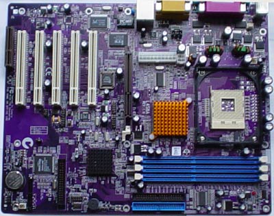
ECS L4S8A Rev. 1: Basic Features
For the first time in quite a while, ECS puts together a fully loaded motherboard. Let's take a look at some of the specs.
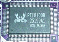
We see that ECS goes with a pretty common LAN chip; Some of the fully featured motherboards we've seen have included some not-so spectacular LAN chips, and ECS's board doesn't really do anything too different by including Realtek's 8100B 10/100 chip. It's no surprise to see Realtek raking up the motherboard wins as we've had nothing but good experiences with the 8100B.
 |
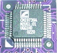 |
ECS goes with C-Media's CMI9739A chip for the onboard audio. This sound chip is a little more unconventional in the motherboards we've reviewed in the last few months, as Realtek's ALC650 or C-media's CMI8738 chip have dominated this space. The 9739A chip is a 6-channel solution much like its predecessor, however at this point we haven't had enough experience with the newcomer to determine its advantages (if any) over the more common 8738.
The L4S8A's I/O configuration is pretty standard. You get two PS/2 ports, two serial ports, one parallel port, two rear USB 2.0 ports, a LAN port, and Mic In/Line In/Line Out ports driven by the on-board CMI9739A chip. We can now confidently say that rear LAN and USB ports are standard on all the latest motherboards, be it a Socket 478 or Socket A motherboard.
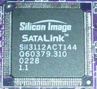 Another
feature we see ECS add to the L4S8A is Serial ATA support. Onboard Serial ATA
is powered by Silicon Image's 3112A chip, the same chip found on Intel's "enthusiast"
board (D845PEBT2) and Epox's 4PEA+. The SI 3112A chip is capable of supporting
two independent Serial ATA devices as well as RAID 0 (striping) and RAID 1 (mirroring).
This is a very nice Serial ATA chip to have, although, as mentioned here before,
onboard Serial ATA chips have to use the limited bandwidth of the PCI bus. Ideally,
motherboard manufacturers would just wait for chipset manufactures to release
chipsets with native support for Serial ATA, which would allow Serial ATA devices
to eat up the bandwidth available directly through the chipset's own I/O links,
which offer much more bandwidth (with today's chipsets, anywhere from 200 to
1000MB/s additional bandwidth, and even more in the future).
Another
feature we see ECS add to the L4S8A is Serial ATA support. Onboard Serial ATA
is powered by Silicon Image's 3112A chip, the same chip found on Intel's "enthusiast"
board (D845PEBT2) and Epox's 4PEA+. The SI 3112A chip is capable of supporting
two independent Serial ATA devices as well as RAID 0 (striping) and RAID 1 (mirroring).
This is a very nice Serial ATA chip to have, although, as mentioned here before,
onboard Serial ATA chips have to use the limited bandwidth of the PCI bus. Ideally,
motherboard manufacturers would just wait for chipset manufactures to release
chipsets with native support for Serial ATA, which would allow Serial ATA devices
to eat up the bandwidth available directly through the chipset's own I/O links,
which offer much more bandwidth (with today's chipsets, anywhere from 200 to
1000MB/s additional bandwidth, and even more in the future).
The Primary and Secondary IDE connectors support two channels each, as is always the case. Unfortunately that means the ECS L4S8A supports no more than four IDE devices, since there is no IDE RAID (just Serial ATA RAID). However, if you don't need to use more than two optical drives, two hard drives, or some other combination thereof in your system, then you should have no problem with the L4S8A's "limited" IDE support.
We see that ECS makes use of a native (chipset) feature, namely FireWire support. This is much better than having a separate FireWire chip, which would end up using the PCI bus's limited bandwidth (much like the Serial ATA chip has to). Instead, FireWire gets to use the SiS 648's interconnect, aka MuTIOL (about 1000MB/s of bandwidth). We should note that ECS takes advantage of the SiS 648's native support for FireWire (1394a) by adding two headers to the L4S8A. There doesn't seem to be a FireWire bracket bundled with the L4S8A, but perhaps ECS simply forgot to include this with our sample.
As is the norm among all modern-day chipsets, USB 2.0 support is included, courtesy of the SiS 963 South Bridge. We'd like to quickly recap the SiS 648 chipset itself, since we haven't done a SiS 648 review in a few weeks. So, as has been covered here before, the SiS 648 includes features such as:
1. AGP 3.0 (AGP 8X) support.
2. 1GB/s North-South Bridge I/O interconnect, aka MuTIOL.
3. Official Northwood-B (533MHz FSB) support.
4. Native support for USB 2.0, 1394a (FireWire), ATA133, Ethernet, and basic 6-channel sound.
5. Unofficial support for DDR400 memory (SiS648 only "officially" supports as high as DDR333 memory).
ECS L4S8A: Board Layout
The ECS L4S8A had only a decent layout, with a good amount of issues we'd like to point out.
ECS positions the ATX (20-pin) connector on the left side of the motherboard. This isn't the best place to locate the ATX connector because it becomes very difficult to uninstall the HSF without having to unhook the ATX connector first because of the thick ATX lines. Most motherboard manufacturers like to ignore the ease of installation aspect of their design unfortunately.
The way the CPU fan header is positioned is also not so ideal and thus quite annoying.
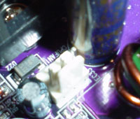
The fan header is located next to two capacitors, one large one and very tiny one, as well as very close to the HSF clamps. This causes a problem if we were to unhook the CPU fan line, as it makes it quite the task to fit your fingers in there without having to tug on the HSF fan wires. This problem is very similar to what we experienced with MSI's 845PE Max2-FIR motherboard.
The ATX12V connector is yet another item that isn't positioned properly. The ATX12V connector is located on the left-hand side of the motherboard, right next to the ATX connector. The reason we don't like this positioning is because the ATX12V line is directly in the path of uninstalling the HSF, meaning you have to unhook the ATX12V line first. The best location for the ATX12V connector is at the very top of the right-hand side of the motherboard, above the DIMM slots. This is also the best place for the ATX connector.
Luckily enough, ECS places the Primary/Secondary IDE connectors above the middle right-hand portion of the motherboard. By doing this, it won't make it difficult for the IDE cables to reach to the uppermost bays of a full-sized ATX case. In addition, there's no chance that the IDE cables will get tangled up with your video card in most cases.
Like most motherboard manufacturers, ECS places the DIMM connectors very close to where your video card would be. By doing this, ECS makes it difficult for you to install/uninstall any memory with your video card installed. Instead, you have to uninstall the video card to install/uninstall any memory (although it does depend on the length of your video card; our test bed's GF4 Ti 4600 was long enough to make this a problem).
Again similar to the MSI 845PE Max2-FIR, ECS places another tiny capacitor in the way of something, this time right next to the AGP lever.

This positioning made it a bit difficult to uninstall the video card without touching the capacitor, although we didn't have to do any dangerous bending this time as we were forced to do with MSI's 845PE board.
The rest of ECS's layout choices aren't too spectacular either. There are two FireWire headers just above the middle PCI slot. By putting the FireWire headers here, ECS brings the potential in for the FireWire bracket wires to get tangled up with other PCI cards that you may install, which isn't good for installation (and even air flow in some ways). The locations of the two USB 2.0 headers aren't much better either. The USB headers are placed very poorly, right smack in the middle of the motherboard just below the AGP 8X slot. If you were to install multiple USB and FireWire brackets on this board, it would be hell to deal with all the wires that would clutter up your case.
ECS L4S8A: BIOS and Overclocking
As is not unusual with modern-day performance motherboards, the ECS L4S8A utilizes Phoenix Technology's Award BIOS.
The PC Health section of the ECS's latest L4S8A BIOS contains an average amount of info.
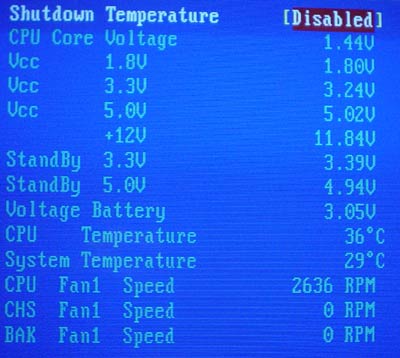
Here you'll be able to find readings on Vcore, PSU readings (all rails), battery voltage, CPU temperature, system temperature, and different types of fan speeds for each of the three fan headers on the board. We see that the reported temperature as read by the PC Health section in this Nov. 6th BIOS hovers around 36-38C, which is only a couple degrees lower than what the norm is for this particular CPU.
We weren't able to do a whole lot of tweaking in the Advanced Chipset Features section of this BIOS, but at least we were able to adjust Command Rate and DRAM timing mode (although this is pretty normal for SiS 648 boards).

You're able to adjust CAS Latency, Command Rate, and DRAM timing mode only. We would have like to have seen other timings as well, but they don't affect performance all that much, so we aren't too disappointed. Interestingly enough, there are DDR400 and DDR400V timing modes available after Ultra mode in the BIOS.

Unfortunately, these options didn't do anything for DDR400 performance, as
we were unable to operate even one stick of Corsair XMS memory at 400MHz no
matter what timings were used. DDR400 and DDR400V timing modes worked well with
memory running at 333MHz, but in both cases there was a performance drop versus
Ultra timing mode, making it pointless to use the DDR400 and DDR400V modes.
There are a ton of memory dividers with the November 6th BIOS; We have found this to be the case with several SiS 648 boards, including the famous Gigabyte 8SG667.

Unfortunately, we were unable to run even at 400MHz with any real reliability and in general, these memory dividers are a complete waste on the L4S8A. The best thing to do if you plan on running this board in spec is to run your FSB at 133MHz with memory running at 333MHz.
The voltage adjustments available in the BIOS were pretty weak with this board. VDIMM was only adjustable as high as 2.62V in 1.2% and 2.0% increments. In reality, this really isn't too terrible, as most memory overclockers usually don't need more than 2.6V. However, it's still a limitation, even though this board can't handle high overclocked memory speeds.
 |
 |
Vcore is adjustable only as high as 1.575V in 1.0% and 2.0% increments. In reality though, the actual max Vcore will only run at 1.525V or so. This is due to the fact that this board undervolts quite a bit; in fact, between 1.44-1.45V when Vcore is set to normal (1.5V is the default Vcore for all pre-C1 stepping Northwood Pentium 4 processors). This is actually quite a limitation for overclockers, as 1.525V isn't that much at all. We would have been satisfied with 1.6V (which is pretty safe).
Thankfully, ECS included an AGP/PCI lock running at 66MHz/33MHz in their latest BIOS update dated November 6 of this year. Previously, in the October 10 BIOS, there was no AGP/PCI lock option. This is a very welcome feature to have for all overclockers, as it protects your AGP and PCI cards from running at too high a frequency, which could potentially damage those cards.
The ECS L4S8A was able to rack up some very impressive FSB overclocking results (for a SiS 648 motherboard). However, it should be noted that this overclock was using a 1:1 divider, and in general performance wasn't as proportionally better as we would have liked compared to stock and officially supported 133MHz FSB and 333MHz memory performance numbers:
|
Front Side Bus Overclocking Testbed |
|
|
Processor:
|
Pentium
4 2.26GHz
|
|
CPU
Vcore:
|
1.5V
(actual)
|
|
Cooling:
|
Intel
Retail HSF & Thermal Pad
|
|
Power
Supply:
|
Enermax
300W
|
With this setup we were able to push the L4S8A to 152MHz FSB. This is the best overclock we've seen out of any SiS 648 motherboard. However, we were forced to run at a 1:1 divider, meaning memory ran no higher than 304MHz effective clock. While this isn't too bad, we were able to run the SiS 648-based Gigabyte 8SG667 at 150MHz FSB and 400MHz effective memory with the exact same setup (we were even able to reliably reach 422MHz memory clock). Therefore, we still think the 8SG667 is the best performer/overclocker out of all the SiS 648 motherboards we've tested so far, and in its highest overclocked state, the fastest SiS 648 motherboard on the market.
ECS L4S8A: Stress Testing
We managed to run quite a few tests on the L4S8A, although we weren't able to do as much as we would have liked due to the poor DDR400 functionality. We still managed to test this board in several different areas and configurations, including
1. Chipset and motherboard stress testing was conducted by running the FSB at 152MHz (1:1 ratio).
2. Memory stress testing was conducted by running RAM at 333MHz with one bank filled as well as as many as was possible from that point on with the most aggressive timings available.
During our FSB overclocking stress tests, we were able to reliably run the L4S8A for 24 hrs straight with Prime95 torture tests running in the background. In addition to the Prime95 stress tests, we reran our entire benchmark suite several times over at 152MHz FSB with great success. Recently, we decided to share some of the general application usage data we've experienced with our motherboards. That is, we simply use the L4S8A like any other computer system; so we run a bunch of pretty common tasks, such as data compression, Word, IE, Outlook, etc. We're happy to report that at 152MHz FSB (1:1 divider), everything ran happily.
We haven't encountered an officially supported DDR333 motherboard that hasn't been able to run one DIMM at 333MHz at aggressive memory timings. The L4S8A is no exception. Here were our results in this conservative DDR333 situation with one Corsair DIMM running at 333MHz with the most aggressive timings possible:
|
Stable
DDR333 Timings |
|
|
Clock
Speed:
|
166MHz
|
|
Timing
Mode:
|
Ultra
|
|
CAS
Latency:
|
2
|
|
Bank
Interleave:
|
N/A
|
|
Precharge
to Active:
|
N/A
|
|
Active
to Precharge:
|
N/A
|
|
Active
to CMD:
|
N/A
|
|
Command
Rate:
|
1T
|
These are great timings, and certainly nothing surprising. We would have like to have seen better options as far as adjusting DRAM timings like Precharge to Active and other such settings, but in general these are very aggressive timings. Besides, timings like Precharge to Active really don't make much of a performance difference on most motherboards, although they are great for stress testing.
A single DIMM operating at 333MHz, CAS 2, CR 1T, and Ultra mode was very easy for the L4S8A. So we moved on to a more aggressive situation, this time with 2 of 3 banks filled. We were able to achieve the following DRAM settings:
|
Stable
DDR333 Timings |
|
|
Clock
Speed:
|
166MHz
|
|
Timing
Mode:
|
Fast
|
|
CAS
Latency:
|
2.5
|
|
Bank
Interleave:
|
N/A
|
|
Precharge
to Active:
|
N/A
|
|
Active
to Precharge:
|
N/A
|
|
Active
to CMD:
|
N/A
|
|
Command
Rate:
|
1T
|
These are decent DRAM timings for two DIMMs; most users should be happy with these results. Disappointingly enough, we did not have as much success with all three banks filled. With all memory banks occupied, we were able to run the following:
|
Stable
DDR333 Timings |
|
|
Clock
Speed:
|
166MHz
|
|
Timing
Mode:
|
Safe
|
|
CAS
Latency:
|
3.0
|
|
Bank
Interleave:
|
N/A
|
|
Precharge
to Active:
|
N/A
|
|
Active
to Precharge:
|
N/A
|
|
Active
to CMD:
|
N/A
|
|
Command
Rate:
|
1T
|
These are certainly very poor timings. In fact, it's not even worth it to run three sticks of memory at these timings, as we discovered that performance was approximately 5-10% lower across the board with most of the programs we ran.
As we normally do, we like to make sure our most aggressive DRAM settings are as stable as possible. Therefore, we ran our usual array of stress tests on the L4S8A, including 24 hrs of Prime95 torture tests at the timings listed in the above three charts. During the time this board was being stressed, we also ran some everyday apps like Word, Outlook, IE, and some data compression here and there. Several runs of SuperPi were tested as well. All in all, we encountered no problems whatsoever.
ECS L4S8A: Tech Support and RMA
For your reference, we will repost our tech support evaluation procedure here:
The way our Tech Support evaluation works is first we anonymously email the manufacturer's tech support address(es), obviously not using our AnandTech mail server to avoid any sort of preferential treatment. Our emails (we can and will send more than one just to make sure we're not getting the staff on an "off" day) all contain fixable problems that we've had with our motherboard. We then give the manufacturer up to 72 hours to respond over business days and will report not only whether they even responded within the time allotted but also if they were successful in fixing our problems. If we do eventually receive a response after the review is published, we will go back and amend the review with the total time it took for the manufacturer to respond to our requests.
The idea here is to encourage manufacturers to improve their technical support as well as provide new criteria to base your motherboard purchasing decisions upon; with motherboards looking more and more alike every day, we have to help separate the boys from the men in as many ways as possible. As usual, we're interested in your feedback on this and other parts of our reviews so please do email us with your comments.
ECS's tech support was fairly good; After sending off our email to ECS's tech
support team, we received a response from their them in just 40 hours flat.
This is an excellent response time. We were pleased to see they were helpful
in diagnosing our problem too, and in general they provided lots of different
phone numbers and email addresses for us to contact them at if we had any other
tech support questions. This type of information can be very helpful.
ECS's RMA policy and warranty are listed below; their motherboards are covered by a relatively standard 1-year warranty. Note that boards from Intel and VIA often carry 3 - 5 year warranty periods whereas most other manufacturers offer only 1 year coverage.
|
ECS's RMA policy is fairly good compared to other motherboard manufacturers,
especially larger ones. However the biggest downside is that you are only allowed
to RMA a board if you purchase directly from ECS; if you buy through any other
vendors or any other channels you are left to deal with them in order to resolve
RMA issues.
Their RMA form asks for the usual amount of information, such as personal info, system specifications, etc.
The Test
|
Performance Test Configuration |
||
| Processor(s): |
Intel
Pentium 4 2.26GHz
|
|
| RAM: |
256MB Samsung DDR333 CAS2.5 Modules
256MB Kingston DDR333 CAS2.5 Modules 256MB Twinmos DDR400 CAS2.5 Modules 256MB Mushkin DDR400 CAS2.5 Modules 256MB Corsair DDR400 CAS2.0 Modules |
|
| Hard Drive(s): |
Western Digital 120GB 7200 RPM
Special Edition (8MB Buffer)
|
|
| Bus Master Drivers: |
Intel Application Accelerator
v2.2.2
SiS Chipset Patches |
|
| Video Card(s): |
ASUS
V8460 Ultra NVIDIA GeForce4 Ti 4600
|
|
| Video Drivers: |
NVIDIA
Detonator 30.82
|
|
| Operation System(s): |
Windows
XP Professional
|
|
| Motherboards: |
ASUS
P4B533-E (845E)
ASUS P4PE (845PE) ASUS P4T533-C (850E) ECS L4S8A (SiS 648) Gigabyte 8SG667 (SiS 648) |
|
All performance tests were run using a 256MB Corsair XMS DDR400 module set to CAS 2-2-2-5 timings. Any other performance-enhancing timings (like Command Rate or Bank Interleave) were enabled in motherboards that contained such timings.
The AnandTech Motherboard Testbed was Sponsored by Newegg. You can buy the components we used to test at www.newegg.com.
Content Creation & General Usage Performance
For our Content Creation & General Usage performance we continue to use SYSMark 2002. The applications benchmarked include:
· Internet Content Generation: Adobe Photoshop® 6.01, Adobe Premiere® 6.0, Microsoft Windows Media Encoder 7.1, Macromedia Dreamweaver 4, and Macromedia Flash 5
· Office Productivity: Microsoft Word 2002, Microsoft Excel 2002, Microsoft PowerPoint 2002, Microsoft Outlook 2002, Microsoft Access 2002, Netscape Communicator® 6.0, Dragon NaturallySpeaking Preferred v.5, WinZip 8.0, and McAfee VirusScan 5.13.
For more information on the methodology and exactly what SYSMark does to generate these performance scores check out BAPCo's SYSMark 2002 Whitepaper.
|
|
Gaming Performance
|
|
Gaming Performance (continued...)
|
|
High End Workstation Performance - SPEC Viewperf 7.0
The latest version of SPEC Viewperf proves to be an excellent stress test for memory bandwidth and overall platform performance as you're about to see. The benchmarks included version 7 of the benchmark suite are:
3ds max (3dsmax-01)
Unigraphics (ugs-01)
Pro/Engineer (proe-01)
DesignReview (drv-08)
Data Explorer (dx-07)
Lightscape (light-05)
For more information on the tests run visit SPEC's page on the new Viewperf benchmark.
|
|
|
High-End Workstation Performance (continued...)
|
|
|
Final Words
All in all, ECS has done quite a fine job with the L4S8A. Let's list exactly what this board offers to the three areas we feel most of our users fall into:
1. For those users that are on a tight budget and simply need a fast and cheap motherboard, the ECS L4S8A isn't bad. Even with Serial ATA, this board isn't supposed to be more than $110 at debut, which is dirt cheap for what you get. Another model, the L4S8A2, is currently selling for just around $90 shipped in the U.S. from a couple of vendors. The only difference between the L4S8A and L4S8A2 is the SI 3112A Serial ATA RAID chip.
2. For those users that are simply interested in a feature-filled, fast, and reasonably priced motherboard, the ECS L4S8A is without a doubt a perfect candidate. You get a combination of Serial ATA RAID (no IDE RAID though), FireWire, sound, LAN, and room for expansion among other features. Besides not having integrated VGA, we would have to call the L4S8A one of the best all-in-one solutions on the market for Socket 478 users.
3. For those users that desire a flexible, feature-filled and overclockable motherboard no matter the price, the ECS L4S8A does a decent job. The overclocking options available in the Award BIOS were fair, but not acceptable for serious tweakers. The L4S8A didn't do too poorly as far as FSB overclocking was concerned (152MHz FSB), but this is nothing compared to the 845PE boards we've seen, even if this overclock was the best out of any SiS 648 motherboard we've tested. Although it's also worth noting that 152MHz FSB was only attainable at a 1:1 divider, meaning memory frequency (and therefore some performance) was sacrificed for a high FSB.
The price of the L4S8A's lower-cost brother, the L4S8A2, is currently around $90 shipped in the U.S. This makes the L4S8A2 one of the best Socket 478 value motherboards on the market. Albatron's PX845PEV Pro and the Epox 4G4A+ are probably the only other modern motherboards that can compete with the ECS L4S8A series in the value Socket 478 market as far as features, performance, price, and tweakability/overclockability are concerned.
We hope you enjoyed our coverage of ECS's L4S8A motherboard. Stay tuned for our SiS 648 roundup in December. Also, watch for our Granite Bay and nForce2 shootouts next week, it should be lots of fun. :)


