Original Link: https://www.anandtech.com/show/956
VIA and SiS Battle for Supremacy: 3-way P4 DDR Motherboard Roundup
by Evan Lieb on July 30, 2002 2:46 AM EST- Posted in
- Motherboards
Out of all the semiconductor industries in existence, there aren’t many with as much competition as the CPU chipset market can claim. There are a grand total of 7 companies producing chipsets for Pentium 4, Athlon XP, or future generation platforms (Intel, AMD, VIA, SiS, NVIDIA, ATI, and ALI). Intel is the largest chipset maker of them all, but two other companies are battling it out for the runner-up position, namely VIA and SiS.
It can be argued that VIA’s rise to success started back in the late 1990’s when Intel was unable to produce enough PC133-compatible Pentium III chipsets. VIA saw this as an opportunity to grow its market share, and took great advantage of it, providing chipsets to vendors that desired them. In addition to this good fortune, VIA was also smart enough to take advantage of the launch of AMD’s brand new microprocessor at the time, the Athlon. VIA was the first chipset company to defy Intel’s wishes and produce an Athlon chipset, and from that point on VIA has completely dominated the Athlon market, solidifying its position with such successes as the KT266A chipset.
However, following closely on VIA’s heels is another vendor by the name of SiS. SiS was once considered to be merely a low-cost, low-profile manufacturer, and was never a major threat to industry leaders Intel and VIA. But now little SiS is gaining big.
SiS’s first real hit arrived on the scene when they introduced their 735 chipset, designed for the Socket A Athlon Thunderbird market. With the release of the SiS 735 in July of last year, SiS was able to claim the best performance out of any DDR Athlon chipset on the market at the time, comfortably besting VIA’s flagship Athlon chipset, the KT266. Not only that, but 735 boards debuted at dirt cheap prices that VIA could not match; this was thanks to SiS’ own fab, whereas VIA outsources all of their production to TSMC. SiS 735 boards hovered around the $70 mark at introduction and only went lower from there. Though there was only one available motherboard based on SiS’s 735 chipset (ECS K7S5A) that was enough to get them going.
With the 735 firmly under its belt, SiS went after bigger markets and that meant the Pentium 4 platform. SiS’s first DDR Pentium 4 chipset, the SiS 645, started off with a bang. Yet again, SiS released a stellar performer with unique and solid features for the time (DDR333 support, etc.) and as usual at dirt cheap prices. Even better, the SiS 645 didn’t suffer the same lack of support in the Pentium 4 market as the SiS 735 did in the Athlon market. Top-tier motherboard manufacturers such as Asus, MSI, and Gigabyte among many others were all over the SiS 645, and eventually its successor the 645DX.
VIA on the other hand is at a great disadvantage to SiS in the Pentium 4 market. VIA is currently fighting a legal battle with Intel over whether it should have to pay a fee for each chipset they produce based on the Pentium 4 bus. Because of VIA’s legal wrangling with Intel, top-tier motherboard manufacturers have steered clear of VIA’s P4X series of chipsets for fear of upsetting Intel. Intel’s influence over motherboard makers has greatly slowed down the adoption of VIA’s P4X chipsets, and consequentially VIA’s market share and profit margins have suffered significantly. SiS on the other hand has a license to produce Pentium 4 compatible chipsets, and is basically in the clear to do as it wishes.
Now that we have a better picture of where VIA and SiS stand, let’s take a look at the first "unofficial" retail Pentium 4 DDR400 motherboards based on the SiS 648 and VIA P4X400 chipsets…
Overview of P4X400 and 648
Compared to its very successful 645DX brother, SiS’s new 648 chipset brings a great deal of new and improved features to the table. Among these features are:
1. AGP 3.0 (8X) support.
2. 1GB/s I/O interconnect, aka MuTIOL
3. Official Northwood-B (533MHz FSB) support
4. Native support for USB 2.0, 1394a (FireWire), ATA133, Ethernet, and basic 6-channel sound.
5. Unofficial support for DDR400 memory (SiS648 only “officially” supports as high as DDR333 memory).
For more detailed information on the SiS 648 chipset, please see our recent article entitled “Taking Advantage of the P4 Situation”.
In addition to "unofficial" DDR400 support, the P4X400 brings over all the same features from the P4X333 chipset we reviewed back in May. At the time of our P4X333 review, we were disappointed, to say the least, that VIA and Intel still hadn’t resolved their licensing conflict over the Pentium 4 bus. Our disappointment over all the legal turmoil stemmed from the fact that the features the P4X333 offered were the best out of any other DDR Pentium 4 chipsets we had seen at the time. The P4X333 brought features like native USB 2.0 and ATA133 support, DDR333 support (through an improved version of the KT333 memory controller), official 533MHz FSB support, an optimized PCI bus implementation, and a new V-link interconnect speed running at 533MB/s.
On another note, one can only wonder what would have happened had Intel and VIA settled their legal disputes before the P4X333 launched. In all likelihood, we would be seeing widespread adoption of the P4X333 (and now the P4X400) by top-tier motherboard makers such as Gigabyte, ASUS, and MSI among others. So while VIA enjoys top-tier mainboard support in the Athlon XP market, their situation in the Pentium 4 market is much more uncomfortable.
Looking at DDR400
With DDR400 memory, the P4X400 and SiS 648 chipsets are able to provide Intel’s Pentium 4 Northwood-B (533MHz FSB) processors a peak bandwidth of about 3.2GB/s. This is the largest available bandwidth the Pentium 4 has ever seen supported by a DDR chipset. Only Intel’s 850E chipset outfitted with dual channel PC1066 RDRAM provides greater theoretical bandwidth than the P4X400 and SiS 648 chipsets do with single channel DDR400.

However, current DDR400 memory is essentially overclocked DDR333 relabeled as DDR400. DDR333 is now a JEDEC-approved specification whereas there is no spec for DDR400, hence the reason why there only exists overclocked DDR333. Generally speaking, with a JEDEC-approved specification comes lower memory latency and better timings than just overclocking a previous technology and relabeling it. Even though DDR333 has considerably less available theoretical bandwidth compared to DDR400, DDR333 is in fact competitive with DDR400 if you purchase the right kind. For example, CAS 2 DDR333 from Samsung will perform more or less equal to the best DDR400 currently available on the market (whose CAS Latency is still no better than 2.5).
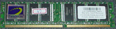
We tested with Twinmos DDR400
If you remember, DDR333 was once in the same situation as DDR400 is in today.
Back then, DDR333 was nothing more than just DDR266 overclocked to DDR333 speeds.
Weeks later, real DDR333 started hitting the streets and with that finally came
some noticeable performance gains over DDR266. If the DDR333 situation of several
months ago has taught us anything, it’s to wait for the real thing. Therefore,
we suggest that everyone wait for real DDR400 to hit the market.
Looking ahead, if JEDEC ever does finally approve a spec for DDR400 memory,
that will likely be the last frequency we see out of DDR-I technology. DDR-I
is clearly reaching its physical limits, and a new design needs to be implemented
to reliably scale past DDR400 speeds. As you might already know, DDR-II is this
new, more scalable design. The current timetable for DDR-II’s initial
availability is mid-2003, but because this timetable is only for first shipments,
DDR-II probably won’t have a significant impact until months later. However,
we have reason to believe that as early this winter we will see DDR-II products
in the form of high-end graphics cards. NVIDIA’s next generation NV30
GPU is rumored to include DDR-II technology, and we’re sure ATI won’t
be snoozing at the wheel in implementing DDR-II for their recently introduced
R300 architecture.
AGP 8X Functionality?
In our P4X333 article back in May of this year, we mentioned that we were unable
to operate the P4X333 using an AGP 8X compatible SiS Xabre 400 video card. We
recently received confirmation from VIA that AGP 8X was indeed broken in the
P4X333 chipset, which is why we couldn’t reliably run the Xabre card at
AGP 8X in our P4X333 board.
The P4X400, however, has functional AGP 8X according to VIA and several motherboard
manufacturers. We have also been told by SiS and other motherboard manufacturers
that AGP 8X is functional on all SiS 648 boards. While we put lots of faith
in the chipset and motherboard maker’s claim that their boards are capable
of AGP 8X, we can’t confirm for certain until we get a hold of a reliable
AGP 8X card to test. We will be able to confirm this in one of our upcoming
roundups.
In addition, when we do finally receive a reliable AGP 8X compliant video card for an extensive period of time, we’ll see if that 2.1 GB/s of peak bandwidth does any good in the real world. However, our feeling is that AGP 8X is going to be just another marketing gimmick for now, worth basically nothing in today’s applications.
The Candidates
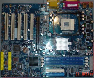
Today we will be looking at a total of 3 different retail motherboards based on the SiS 648 and VIA P4X400 chipsets. These boards include the following:
1. VPSD P4PB 400 (VIA P4X400)
2. Shuttle AS45GTR (SiS 648)
3. Soltek 85ERV-L (VIA P4X400)
During our tests, we discovered that all 3 retail boards were unable to reliably operate using Twinmos DDR400 memory. No matter how conservative we set the memory timings, none of the boards were able to operate DDR400 without crashing consistently. Therefore, we saw no point in listing the few benchmarks these boards were able to complete with DDR400 memory. It’s interesting to note that the SiS 648 reference board running DDR400 memory at stock speeds and timings was perfectly rock solid during all the benchmarks we performed on it. We experienced zero crashes, random reboots or anything else of the sort. Yet, Shuttle’s SiS 648 board was no where near as reliable with DDR400 as the 648 reference board was. We’ll be talking this over with motherboard makers very soon.
On another note, we should mention that the VPSD P4PB 400 has a much more interesting brother coming along soon, going by the name of VPSD P4PB Ultra. The P4PB Ultra comes with quite an extensive feature set; this includes onboard ATA133 Promise RAID (0+1 arrays), support for up to 10 USB 2.0 ports, onboard sound in the form of C-media's 6-channel 8738 chip, and 10/100 Ethernet in the form of VIA’s Rhine III VT6105 chip. Additionally, the P4PB Ultra has a total of 6 PCI slots and 3 DIMM slots.
VPSD P4PB 400
| Motherboard Specifications |
|
|
CPU
Interface |
Socket-478 |
|
Chipset |
VIA
P4X400 North Bridge VIA VT8235 South Bridge |
|
Bus
Speeds |
100
- 200MHz (in 1MHz increments) |
|
Core
Voltages Supported |
up
to 1.85V |
|
I/O
Voltages Supported |
N/A |
|
DRAM
Voltages Supported |
up
to 2.8V |
|
Memory
Slots |
3
184-pin DDR DIMM Slots |
|
Expansion
Slots |
1
AGP 8X Slot 5 PCI Slots |
|
Onboard
RAID |
N/A |
|
Onboard
USB 2.0/IEEE-1394 |
USB2
Supported through South Bridge |
|
Onboard
LAN |
VIA
Rhine III VT6105 |
|
Onboard
Audio |
VIA
VT1616 6-Channel AC'97 Codec |

VIA decided to design two different P4X400-based motherboards for two separate markets this time around. The first P4X400-based motherboard (the board we’ll be testing today) is called the P4PB 400. VIA’s second P4X400 motherboard is still in the works, dubbed the P4PB Ultra.
While the P4PB 400 isn’t as feature-rich as some of the Intel 845E and 845G boards we’ve tested in the past, it still packs quite an acceptable punch. The P4PB 400 includes support for up to 6 USB 2.0 ports, 2 ATA133 IDE channels, and onboard LAN and sound chips. The P4PB 400 is also quite flexible, with support for as much as 3.0GB of memory using any of the 3 DIMM slots onboard. In addition, there are 5 PCI slots ready for additional expansion.
The P4PB 400 also includes VIA’s onboard VT6306 IEEE 1394 controller. Unfortunately our board was not outfitted with VIA’s FireWire chip for some reason, but we were assured that all future VIA P4PB 400 boards will come with onboard 1394a FireWire.
There isn’t much special to say about the other onboard chips. VIA’s
LAN chip supports a basic feature-set; wake-on-LAN, remote bootability and multiple
VLAN. VIA’s onboard 6-channel sound wasn’t all that terrible either.
Stressing the P4PB
The general reliability and stability of a motherboard is difficult to gauge
in a single review over a matter of days. In fact, one method of measuring reliability
is to examine the individual layers of a PCB by breaking apart a motherboard
and examining the board under a microscope. Obviously, we don’t have the
ability do such a test, so we decided to instead share our more practical stress
test results. We felt that this way our readers will be able to come up with
their own conclusions.
We started stress testing the P4PB 400 by running Prime95 Torture tests around
the clock using DDR333 CL2.5 memory from Samsung. We also ran all the latest
video games to make sure the P4PB 400 could handle intensive DX8 gaming. Finally,
we decided to be a little more aggressive, so we went into the BIOS and adjusted
the memory timings. We switched to Turbo mode and went down to CL2. All in all
though, none of the aggressive timings we used fazed the P4PB 400.
However, some problems cropped up once we started testing DDR400 memory. First off, one of the 3 DIMM slots was completely unable to operate DDR400; it wouldn't even boot into Windows XP. We don’t know the exact cause for this malfunction, but we are working with VIA to pinpoint the issue.
Despite this anomaly, we were able to operate the DDR400 memory in the other
two DIMM slots available on the P4PB 400. With DDR400 in either of the two slots,
we were able to boot into Windows XP and run some of the stress tests and benchmarks
we needed for DDR400 scores. Unfortunately, the P4PB 400 failed to complete
SYSMark 2002 among other benchmarks, even after several tries. But even though
the DDR400 memory was mostly operational using the 2 other slots, it definitely
wasn't as trouble free as we would have preferred (random crashes and reboots
galore).
Overclocking the P4PB
The P4PB 400 comes with a few friendly overclocking options in its BIOS. One of these options lets you raise CPU core voltage as high as 1.85V. While raising Vcore is a good way of ensuring stability when overclocking, you generally don’t want to raise the core voltage more than 10 – 15%, as it can permanently damage your CPU.
Other overclocking options in the BIOS include being able to raise DDR voltage as high as 2.8V, AGP voltage tweaks up to 1.8V, and a 100-200MHz adjustable FSB (in 1MHz increments). Unfortunately there is no option for locking the AGP/PCI bus at 66MHz/33MHz, which is a must for many overclockers.
Though some of the P4PB 400's results might seem quite poor, it’s hard to get a totally accurate picture of stability and reliability when testing a motherboard for a short period of time using only one of the many P4PB 400 motherboards in existence. Over the long haul (months and months of stress testing) you should be able to assess, in general, how stable and how much potential your motherboard is capable of producing, especially if you’re able to test many of the exact same motherboards over the same period of time. We can only share our results as a guide to help you in your decision making process.
Shuttle AS45GTR
| Motherboard Specifications |
|
|
CPU
Interface |
Socket-478 |
|
Chipset |
SiS
648 North Bridge SiS 963 South Bridge |
|
Bus
Speeds |
100
- 165MHz (in 1MHz increments) |
|
Core
Voltages Supported |
up
to 1.85V |
|
I/O
Voltages Supported |
N/A |
|
DRAM
Voltages Supported |
up
to 2.8V |
|
Memory
Slots |
3
184-pin DDR DIMM Slots |
|
Expansion
Slots |
1
AGP 8X Slot 5 PCI Slots |
|
Onboard
RAID |
HighPoint
HPT372 RAID Controller |
|
Onboard
USB 2.0/IEEE-1394 |
USB2
Supported Through South Bridge IEEE-1394 Supported Through South Bridge |
|
Onboard
LAN |
N/A |
|
Onboard
Audio |
Realtek
ALC650 6-Channel AC'97 Codec |
Serial
ATA |
Marvell
88i8030 |
Shuttle isn’t usually the first motherboard maker to release products
based on the latest chipset technology. However, in the case of the Shuttle
AS45GTR motherboard, things are quite different.
Shuttle was the very first motherboard manufacturer to market with a SiS 648-based
board. But that’s not what makes the AS45GTR impressive, not by any means.
The AS45GTR’s features are exceptional among Pentium 4 motherboards.
To start off with, Shuttle integrates IDE RAID in the form of Highpoint’s
372 chip, which supports RAID 0 and 1 arrays. The majority of users should be
happy with the onboard RAID options even though it lacks RAID 0+1 support. In
addition to RAID, you can connect up to a maximum of four IDE devices (one Master
and one Slave per channel).
The AS45GTR also leverages the features native to the SiS 963 South Bridge; that includes USB 2.0, 1394a (FireWire), ATA133, and 6-channel sound. The only feature Shuttle did not utilize that the SiS 693 natively supports is the Ethernet controller. With all these native features, you can connect up to 6 USB2.0 devices and 3 FireWire devices in addition to ATA133 RAID arrays or just regular ATA133 hard drives.
The most unique feature the AS45GTR integrates is a Serial ATA chip, dubbed the Marvel 88i8030. You have the option of connecting as many as two SATA drives to the AS45GTR via two tiny black SATA connectors located on the bottom right corner of the board. One of the many reasons we like the idea of SATA is the fact that SATA cables are extremely small compared to the thick and airflow-constricting IDE cables that we’ve all had to deal with.
Although SATA hard drives will be quite difficult to find in the coming months, it’s certainly not a bad thing to have SATA support onboard. You can expect to see an in depth review of Serial ATA the moment we can get our hands on drives, so don’t worry.
Though the AS45GTR’s features are certainly tempting, we have learned in the past that pricing is an important issue. But if you think that getting the newest chipset on the block in addition to onboard sound, FireWire, USB 2.0, RAID, and SATA would cost more than just a pretty penny, you’re wrong. Shuttle says this baby will debut at a measly $120.
In terms of layout, the Shuttle AS45GTR isn’t anything particularly special. All the IDE and Floppy connectors as well as the 4-pin ATX12V and 20-pin ATX lines are positioned well. The only issue with have with the layout of this board is the location of the DIMM slots, which are placed a little too closely to the AGP slot. In general though, we liked the layout.
Another interesting aspect of the AS45GTR’s layout is the addition of
a black passive heatsink over the SiS 693 South Bridge. This isn’t all
that necessary, but it’s certainly not a bad thing to add extra cooling
to such a vital part of your motherboard, so we can’t complain.
Overclocking & Stressing the AS45GTR
Shuttle had overclockers in mind for the most part when they designed this board; you have the option of raising Vcore to a sizzling 1.85V and DDR voltage as high as 2.75V. There are also four different CPU:Memory ratio options, which includes 4:3, 1:1, 4:5, and 2:3. In addition, you can adjust the FSB in 1MHz increments between 100-165MHz, which isn’t all that stellar (especially if you have a Northwood-B processor), but it’s acceptable for most nonetheless. Unfortunately, we were unable to find an option for locking the AGP and PCI buses at 66MHz and 33MHz. All in all though, the AS45GTR provides offers a decent overclocking feature set.
To stress the AS45GTR we ran Prime95 torture tests for a full 24 hours straight using Samsung DDR333 memory at default (i.e. conservative) timings. The board never failed a single test. We weren’t completely satisfied yet, so we adjusted memory timings to more aggressive levels, like bumping it up to Turbo mode and lowering CAS Latency down to 2 (from CL2.5). Yet again, the Shuttle board successfully completed all Prime95 torture tests and seamlessly ran all other applications we threw at it (including various DX8 games, DivX, etc.).
Soltek 85ERV
| Motherboard Specifications |
|
|
CPU
Interface |
Socket-478 |
|
Chipset |
VIA
P4X400 North Bridge VIA VT8235 South Bridge |
|
Bus
Speeds |
100
- 200MHz (in 1MHz increments) |
|
Core
Voltages Supported |
up
to 1.85V |
|
I/O
Voltages Supported |
N/A |
|
DRAM
Voltages Supported |
up
to 2.8V |
|
Memory
Slots |
3
184-pin DDR DIMM Slots |
|
Expansion
Slots |
1
AGP 8X Slot 6 PCI Slots |
|
Onboard
RAID |
N/A |
|
Onboard
USB 2.0/IEEE-1394 |
USB2
Supported through South Bridge |
|
Onboard
LAN |
N/A |
|
Onboard
Audio |
AC'97
Codec |

The Soltek 85ERV packs quite a plain set of features and options, in addition to utilizing VIA’s P4X400 chipset.
The 85ERV adds support for as many as 6 USB 2.0 ports and includes other features like AC’97 sound and lots of room for expansion with 6 PCI slots in addition to as much as 3.0 GB of DDR333 memory.
The 85ERV also comes with some nice overclocking options. Some of these include adjustable FSB speeds in 1MHz increments all the way up to 200MHz, VDIMM options up to 2.8V, and Vcore adjustments as high as 1.85V. Unfortunately, this board did not have an option for locking the AGP and PCI buses at 66MHz/33MHz as we had hoped.
The 85ERV’s layout is fairly well thought out. One of the layout choices we were pleased to see added to this board was a plastic plate beneath the CPU Socket. This is an important feature for Pentium 4 motherboards, as pressure from your CPU’s heatsink may bend your board, which isn’t exactly ideal. This is more of an issue for the larger Pentium 4 heatsinks that don’t necessarily follow Intel’s guidelines for pressure and mounting. Admittedly, we have not heard of any major incidents where pressure from the CPU heatsink on the motherboard caused serious damage but it is a good precaution.
Another addition we liked to see was the placement of capacitors around the heatsink. In the 85ERV’s case, the placement of the capacitors was such that uninstalling the heatsink was a breeze, since the capacitors weren’t impeding the uninstallation of the heatsink clamps.
We do have some complaints about the layout of this board, although they’re quite minor ones. For example, just as with the Shuttle AS45GTR, the placement of the DIMM slot connectors are just a little too close to the AGP slot. If you’re using a video card about the length of a GeForce3 or Radeon 8500, you may have to remove the card to insert your RAM. We also would have liked to have seen an AGP retention hook to hold the video card in place, although that’s not too major of an issue for most end users since it’s rare that you ship your computer around.
Overclocking & Stressing the 85ERVAgain, Prime95 was our application of choice for stress testing the Soltek 85ERV. After nearly 24 hours, the Soltek board was able to successfully complete all Prime95 torture tests we ran. Just as we did with previous motherboards, we adjusted the Samsung DDR333 memory timings to more aggressive settings like CL2 and Turbo mode. The Soltek board handled it like a champ.
As we mentioned before, all 3 retail boards we tested could not reliably operate DDR400 memory. The Soltek 85ERV is no different. We were unable to complete any benchmarks with the Twinmos memory, and the system in general was just unstable with DDR400. The issues with DDR400 with this board were more severe than the VPSD P4PB 400 and Shuttle AS45GTR’s issues were with DDR400, but in all 3 cases, none were particularly stable.
As we expected, we encountered numerous problems once we filled all 3 DIMM slots with DDR333 memory. General system stability was unpredictable; sometimes we would be able to run general applications and complete certain benchmarks, and sometimes the system would randomly reboot or just freeze.
The debut price of the Soltek 85ERV should be around $100. Even though that’s not too bad of a deal for what you get, there are many other boards on the market with better features for close to the same price. Just about any 845E/G board and most 645DX/648 boards come with better features and options than the Soltek 85ERV does, and for a very similar price. And even if you aren’t into onboard features, there are better plain-vanilla boards to choose from than Soltek 85ERV.
The Test
| Performance Test Configuration |
||
| Processor(s): | Intel
Pentium 4 2.26B |
|
| RAM: | 256MB Samsung DDR333 CAS2.5 module (M368L3223CTL-C (L) B3) 256MB Twinmos DDR400 CAS2.5 module |
|
| Hard Drive(s): | Western
Digital 120GB 7200 RPM Special Edition (8MB Buffer) |
|
| Bus Master Drivers: |
VIA 4-in-1 4.38v |
|
| Video Card(s): | NVIDIA
GeForce3 Ti 200 |
|
| Video Drivers: | NVIDIA
Detonator 29.42 |
|
| Operation System(s): | Windows
XP Professional |
|
The AnandTech Motherboard Testbed was Sponsored by Newegg. You can buy the components we used to test at www.newegg.com.
Content Creation & General Usage Performance
SYSMark has become a solid measurement of overall system performance since its induction into our benchmarking suite. Although the Internet Content Creation suite caters to more of a niche market, the Office Productivity tests are a perfect measurement of overall system performance in the applications all of us use on a daily basis.
The applications benchmarked include:
· Internet Content Generation: Adobe Photoshop® 6.01, Adobe Premiere® 6.0, Microsoft Windows Media Encoder 7.1, Macromedia Dreamweaver 4, and Macromedia Flash 5
· Office Productivity: Microsoft Word 2002, Microsoft Excel 2002, Microsoft PowerPoint 2002, Microsoft Outlook 2002, Microsoft Access 2002, Netscape Communicator® 6.0, Dragon NaturallySpeaking Preferred v.5, WinZip 8.0, and McAfee VirusScan 5.13.
For more information on the methodology and exactly what SYSMark does to generate these performance scores check out BAPCo's SYSMark 2002 Whitepaper.
|
|
As you can expect, there's little performance difference between boards based on the same chipset. What ends up being somewhat surprising is the close performance between the SiS 648 and the P4X400.
Quake III Arena Performance
Quake III's usefulness as a gaming benchmark has diminished mostly because of the fact that we're able to consistently produce frame rates over 300 fps at 1024x768 with the fastest video cards. But as the benchmark becomes less GPU limited, it becomes a perfect candidate for CPU and platform tests such as this one.
|
Unreal Tournament 2003 Performance - High Detail
We introduced the latest Unreal Tournament 2003 benchmark in our GPU Shootout article a few weeks back and we're continuing to use it as an example of a next-generation game test.
We benchmarked under two different levels and detail settings; the first was DM-Antalus with High Detail settings, an overly GPU bound benchmark, and the second was DM-Asbestos with Medium Detail settings.
|
|
Unreal Tournament 2003 Performance - Medium Detail
|
|
The race continues to be a close one under all of our UT2003 tests.
High End Workstation Performance - SPEC Viewperf 7.0
The latest version of SPEC Viewperf proves to be an excellent stress test for memory bandwidth and overall platform performance as you're about to see. The benchmarks included version 7 of the benchmark suite are:
3ds max (3dsmax-01)
Unigraphics (ugs-01)
Pro/Engineer (proe-01)
DesignReview (drv-08)
Data Explorer (dx-07)
Lightscape (light-05)
For more information on the tests run visit SPEC's page on the new Viewperf benchmark.
|
|
|
High End Workstation Performance - SPEC Viewperf 7.0 (continued)
|
|
|
To summarize, the 648 and P4X400 boards were pretty close in most of the SPEC benchmarks we ran, but the SiS 648 boards clearly take the lead in the remaining two tests. This is the only situation where we see P4X400 boards lag a good deal behind their competition.
Final Words
As proven by our benchmark results, DDR400 doesn’t exactly add a lot of extra performance to the Pentium 4 platform, in addition to not being fully operational with any of the motherboards we used (the SiS 648 Reference board is the exception). Again, this can probably be attributed to the fact that JEDEC has yet to approve an official specification for this memory type and lower latency DDR400 chips are not prevalent enough. The lack of a memory spec makes validation more than just a trivial matter (although validating memory compatibility has never been trivial). Therefore, because there is no spec for DDR400 memory at the moment, we shouldn’t really expect to see current motherboards working well with “fake” DDR400 memory.
If you’ve been keeping up on your news lately, you’ve probably read that VIA, SiS, and NVIDIA are all planning on cooperating with Samsung on attaining a steady flow of DDR400 supplies. At this early stage, it’s clear that these chipset companies will be all over real DDR400 if JEDEC grants approval for the spec. Chipset vendors will fully support DDR400 memory if it does get finalized, and with that we’re sure to see better compatibility and some noticeable performance gains on the Pentium 4 platform.
In the end, all of us can expect to see companies like VIA and SiS continuously
battling it out for the performance crown in an increasing cutthroat industry.
And to that we say good luck and Godspeed.


