Original Link: https://www.anandtech.com/show/8355/intel-broadwell-architecture-preview
Intel Broadwell Architecture Preview: A Glimpse into Core M
by Ryan Smith on August 11, 2014 12:01 PM EST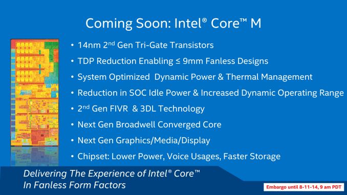
With Haswell Refresh fully behind us and 2014 now in to its second half, Intel is turning their attention to their next generation of products and processes. Intel’s tick-tock methodology coupled with the long development periods of new products means that the company has several projects in flight at any given time. So while we have seen the name Broadwell on Intel’s roadmaps for some time now, the reality of the situation is that we know relatively little about Intel’s next generation architecture and the 14nm process that it is the launch vehicle for.
Typically we would see Intel unveil the bulk of the technical details of their forthcoming products at their annual Intel Developer Forum, and with the next IDF scheduled for the week of September 9th we’ll see just that. However today Intel will be breaking from their established standards a bit by not waiting until IDF to deliver everything at once. In a presentation coinciding with today’s embargo, dubbed Advancing Moore’s Law in 2014, Intel will be offering a preview of sorts for Broadwell while detailing their 14nm process.
Today’s preview and Intel’s associated presentation are going to be based around the forthcoming Intel Core M microprocessor, using the Broadwell configuration otherwise known at Broadwell-Y. The reason for this is a culmination of several factors, and in all honesty it’s probably driven as much by investor relations as it is consumer/enthusiast relations, as Intel would like to convince consumer and investor alike that they are on the right path to take control of the mobile/tablet market through superior products, superior technology, and superior manufacturing. Hence today’s preview will be focused on the part and the market Intel feels is the most competitive and most at risk for the next cycle: the mobile market that Core M will be competing in.
To that end Intel’s preview is very much a preview; we will see bits and pieces of Broadwell’s CPU architecture, GPU architecture, and packaging, along with information about Intel’s 14nm process. However this isn’t a full architecture preview or a full process breakdown. Both of those will have to wait for Intel’s usual forum of IDF.
Diving into matters then, Core M will be launch vehicle for Broadwell and will be released for the holiday period this year. In fact Intel is already in volume production of the Broadwell-Y CPU and production units are shipping to Intel’s customers (the OEMs) to begin production and stockpiling of finished devices for the holiday launch.
Intel’s decision to initially focus Broadwell on the mobile market comes as the company takes the next step in their plan to extend into the Core processor series into these devices. Arguably, Intel has been slow to response to the rise of ARM devices, whose rapid rise has undercut traditional PC sales and quickly become the biggest threat to Intel’s processor dominance in some number of years. Intel is far from doomed right now, but even they see the potential farther down the line if they do not act.
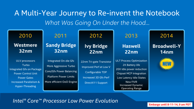
Intel for their part has responded, but it has taken a step-by-step (multi-year) process that has seen the company progressively build smaller and less power hungry CPUs in order to fit the needs of the mobile market. Since Intel integrated their graphics on-die with Sandy Bridge in 2011, the company has continued to tweak the designs of their products, with Ivy Bridge and Haswell generation products introducing further optimizations and new manufacturing processes. Now on their latest iteration with Broadwell, the company believes they’re turning a corner and have the technology they need to be a leader in the high performance mobile market. It's important to note that despite Intel's best intentions here, Broadwell and Core M remain targeted at premium devices. You won't see these parts in cheap tablets. The duty of doing battle with ARM remains Atom's alone.
Many of these changes ultimately amount to boosting performance and reducing power consumption to a point where power and heat are where they need to be for mobile form factors, either through process efficiency improvements or through better power management and wider dynamic ranges – boosting where it matters and doing a better job of idling between tasks. However as Intel has discovered they not only need to be able to meet the TDP requirements of a tablet but they need to be able to meet the size requirements too. A particularly daunting task when the entire thickness of a device needs to be under 10mm, and the CPU thinner yet.
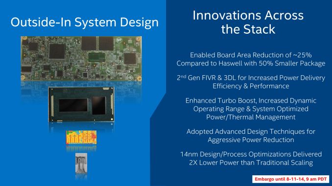
As a result, coupled with Core M’s performance improvements and power reductions is a strong emphasis on the size of the processor package itself and what Intel could do to reduce it. Intel calls this an outside-in system design, with various parts of Intel focusing on everything from the size of the logic board needed to hold the processor to the thickness of the processor die itself. In the following pages we’ll take a look at Intel’s efforts to get slim, but to kick things off we have a picture of Broadwell-Y from Computex 2014.
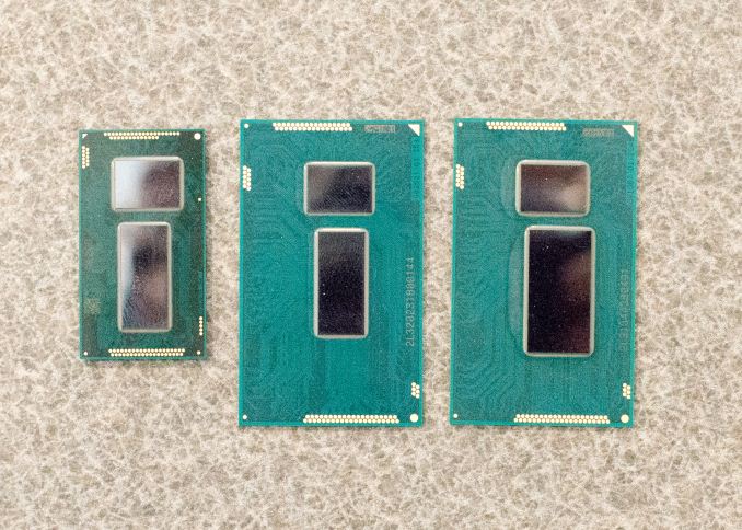
From left to right: Broadwell-Y (Core M), Broadwell ULT/ULX and Haswell ULT/ULX
Intel wants a greater foothold in the mobile market and they want it badly. And with Broadwell-Y they believe they finally have what they need to accomplish that goal.
Broadwell CPU Architecture
We’ll kick off our look at Broadwell-Y with Broadwell’s CPU architecture. As this is a preview Intel isn’t telling us a great deal about the CPU at this time, but they have given us limited information about Broadwell’s architectural changes and what to expect for performance as a result.
With Broadwell Intel is at the beginning of the next cycle of their tick-tock cadence. Whereas tock products such as Haswell and Sandy Bridge designed to be the second generation of products to use a process node and as a result are focused on architectural changes, tick products such as Ivy Bridge and now Broadwell are the first generation of products on a new process node and derive much (but not all) of their advantage from manufacturing process improvements. Over the years Intel has wavered on just what a tick should contain – it’s always more than simply porting an architecture to a new process node – but at the end of the day Broadwell is clearly derived from Haswell and will be taking limited liberties in improving CPU performance as a result.
| Intel's Tick-Tock Cadence | |||||
| Microarchitecture | Process Node | Tick or Tock | Release Year | ||
| Conroe/Merom | 65nm | Tock | 2006 | ||
| Penryn | 45nm | Tick | 2007 | ||
| Nehalem | 45nm | Tock | 2008 | ||
| Westmere | 32nm | Tick | 2010 | ||
| Sandy Bridge | 32nm | Tock | 2011 | ||
| Ivy Bridge | 22nm | Tick | 2012 | ||
| Haswell | 22nm | Tock | 2013 | ||
| Broadwell | 14nm | Tick | 2014 | ||
| Skylake | 14nm | Tock | 2015 | ||
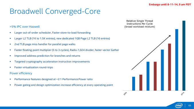
All told, Intel is shooting for a better than 5% IPC improvement over Haswell. This is similar to Ivy Bridge (4%-6%), though at this stage in the game Intel is not talking about expected clockspeeds or the resulting overall performance improvement. Intel has made it clear that they don’t regress on clockspeeds, but beyond that we’ll have to wait for further product details later this year to see how clockspeeds will compare.
To accomplish this IPC increase Intel will be relying on a number of architectural tweaks in Broadwell. Chief among these are bigger schedulers and buffers in order to better feed the CPU cores themselves. Broadwell’s out-of-order scheduling window for example is being increased to allow for more instructions to be reordered, thereby improving IPC. Meanwhile the L2 translation lookaside buffer (TLB) is being increased from 1K to 1.5K entries to reduce address translation misses.
The TLBs are also receiving some broader feature enhancements that should again improve performance. A second miss handler is being added for TLB pages, allowing Broadwell to utilize both handlers at once to walk memory pages in parallel. Otherwise the inclusion of a 1GB page mode should pay off particularly well for servers, granting Broadwell the ability to handle these very large pages on top of its existing 2MB and 4K pages.
Meanwhile, as is often the case Intel is once again iterating on their branch predictor to cut down on missed branches and unnecessary memory operations. Broadwell’s branch predictor will see its address prediction improved for both branches and returns, allowing for more accurate speculation of impending branching operations.
Of course efficiency increases can only take you so far, so along with the above changes Intel is also making some more fundamental improvements to Broadwell’s math performance. Both multiplication and division are receiving a performance boost thanks to performance improvements in their respective hardware. Floating point multiplication is seeing a sizable reduction in instruction latency from 5 cycles to 3 cycles, and meanwhile division performance is being improved by the use of an even larger Radix-1024 (10bit) divider. Even vector operations will see some improvements here, with Broadwell implementing a faster version of the vector Gather instruction.
Finally, while it’s not clear whether these will be part of AES-NI or another instruction subset entirely, Intel is once again targeting cryptography for further improvements. To that end Broadwell will bring with it improvements to multiple cryptography instructions.
Meanwhile it’s interesting to note that in keeping with Intel’s power goals for Broadwell, throughout all of this Intel put strict power efficiency requirements in place for any architecture changes. Whereas Haswell was roughly a 1:1 ratio of performance to power – a 1% increase in performance could cost no more than a 1% increase in power consumption – Broadwell’s architecture improvements were required to be at 2:1. While a 2:1 mandate is not new – Intel had one in place for Nehalem too – at the point even on the best of days meaningful IPC improvements are hard to come by at 1:1, never mind 2:1. The end result no doubt limited what performance optimizations Intel could integrate into Broadwell’s design, but it also functionally reduces power requirements for any given performance level, furthering Intel’s goals in getting Core performance in a mobile device. In the case of Broadwell this means Broadwell’s roughly 5% performance improvement comes at a cost of just a 2.5% increase in immediate power consumption.
With that said, Intel has also continued to make further power optimizations to the entire Broadwell architecture, many of which will be applicable not just to Core M but to all future Broadwell products. Broadwell will see further power gating improvements to better shut off parts of the CPU that are not in use, and more generalized design optimizations have been made to reduce power consumption of various blocks as is appropriate. These optimizations coupled with power efficiency gains from the 14nm process are a big part of the driving force in improving Intel’s power efficiency for Core M.
Broadwell GPU Architecture
While Intel’s tick products are relatively conservative on the CPU side, the same cannot be said for the GPU side. Although the same general tick-tock rules apply to GPUs as well as they do CPUs – the bigger architectural changes are on the tock – the embarrassingly parallel nature of graphics coupled with the density improvements from newer process nodes means that even in a tick Intel’s GPU improvements are going to be substantial. And Broadwell will be no exception.
From a high level overview, Broadwell’s GPU is a continuation of the Intel Gen7 architecture first pioneered in Ivy Bridge and further refined for Gen7.5 in Haswell. While there are some important underlying changes that we’ll get to in a moment, at a fundamental level this is still the same GPU architecture that we’ve seen from Intel for the last two generations, just with more features, more polish, and more optimizations than ever before.
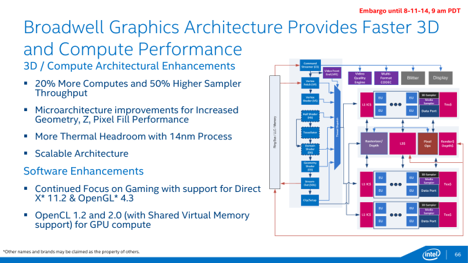
In terms of functionality Broadwell’s GPU has been upgraded to support the latest and greatest graphics APIs, an important milestone for Intel as this means their iGPU is now at feature parity with iGPUs and dGPUs from AMD and NVIDIA. With support for Direct3D feature level 11_2 and Intel’s previous commitment to Direct3D 12, Intel no longer trails AMD and NVIDIA in base features; in fact with FL 11_2 support they’re even technically ahead of NVIDIA’s FL 11_0 Kepler and Maxwell architectures. FL 11_2 is a rather minor update in the long run, but support for it means that Intel now supports tiled resources and pre-compiled shader headers.
Meanwhile on the compute front, Intel has confirmed that Broadwell’s GPU will offer support for OpenCL 2.0, including OpenCL’s shared virtual memory. OpenCL 2.0 will bring with it several improvements that allow GPUs to be more robust compute devices, and though Intel doesn’t have a programming paradigm comparable to AMD’s HSA, SVM none the less affords Intel and OpenCL programmers the chance to better leverage Broadwell’s CPU and GPU together by directly sharing complex data structures rather than copying them around.
Digging deeper however quickly exposes that Intel hasn’t left their GPU architecture entirely alone. Broadwell-Y, like Haswell-Y before it, implements a single slice configuration of Intel’s GPU architecture. However the composition of a slice will be changing for Broadwell, and this will have a significant impact on the balance between various execution units.
| Low Level Architecture Comparison | |||||||||||||||||
| AMD GCN | NVIDIA Maxwell | Intel Gen7.5 Graphics | Intel Gen8 Graphics | ||||||||||||||
| Building Block | GCN Compute Unit | Maxwell SMM | Sub-Slice | Sub-Slice | |||||||||||||
| Shader Building Block | 16-wide Vector SIMD | 32-wide Vector SIMD | 2 x 4-wide Vector SIMD | 2 x 4-wide Vector SIMD | |||||||||||||
| Smallest Implementation | 4 SIMDs | 4 SIMDs | 10 SIMDs | 8 SIMDs | |||||||||||||
| Smallest Implementation (ALUs) | 64 | 128 | 80 | 64 | |||||||||||||
In Haswell-Y Intel used a GT2 configuration, which was composed of a single slice that in turn contained 2 sub-slices. In Intel’s GPU architecture the sub-slice is the smallest functional building block of the GPU, containing the EUs (shaders) along with caches and texture/data/media samplers. Each EU in turn was composed of 2 4-wide vector SIMDs, with 10 EUs per sub-slice.
For Broadwell Intel is not changing the fundamental GPU architecture, but they are rebalancing the number of EUs per sub-slice and increasing the number of sub-slices overall. As compared to Haswell, Broadwell’s sub-slices will contain 8 EUs per sub-slice, with a complete slice now containing 3 sub-slices. Taken altogether this means that whereas Haswell-Y was a 2x10EU GPU, Broadwell-Y will be a 3x8EU GPU.
The ramifications of this is that not only is the total number of EUs increased by 20% from 20 to 24, but Intel has greatly increased the ratio of L1 cache and samplers relative to EUs. There is now 25% more sampling throughput per EU, with a total increase in sampler throughput (at identical clockspeeds) of 50%. By PC GPU standards increases in the ratio of samplers to EUs is very rare, with most designs decreasing that ratio over the years. The fact that Intel is increasing this ratio is a strong sign that Haswell’s balance may have been suboptimal for modern workloads, lacking enough sampler throughput to keep up with its shaders.
Moving on, along with the sub-slices front end and common slice are also receiving their own improvements. The common slice – responsible for housing the ROPs, rasterizer, and a port for the L3 cache – is receiving some microarchitecture improvements to further increase pixel and Z fill rates. Meanwhile the front end’s geometry units are also being beefed up to increase geometry throughput at that end.
Much like overall CPU performance, Intel isn’t talking about overall GPU performance at this time. Between the 20% increase in shading resources and 50% increase in sampling resources Broadwell’s GPU should deliver some strong performance gains, though it seems unlikely that it will be on the order of a full generational gain (e.g. catching up to Haswell GT3). What Intel is doing however is reiterating the benefits of their 14nm process in this case, noting that because 14nm significantly reduces GPU power consumption it will allow for more thermal headroom, which should further improve both burst and sustained GPU performance in TDP-limited scenarios relative to Haswell.
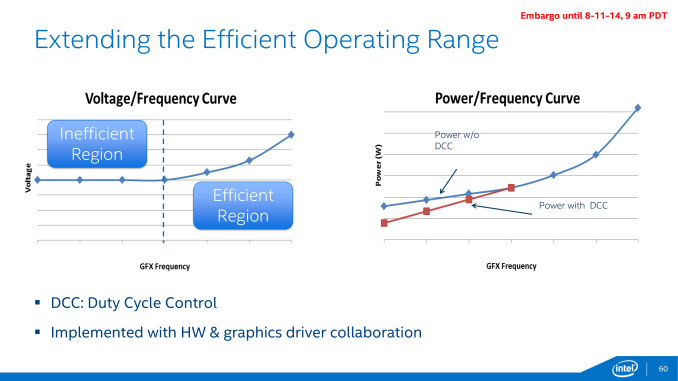
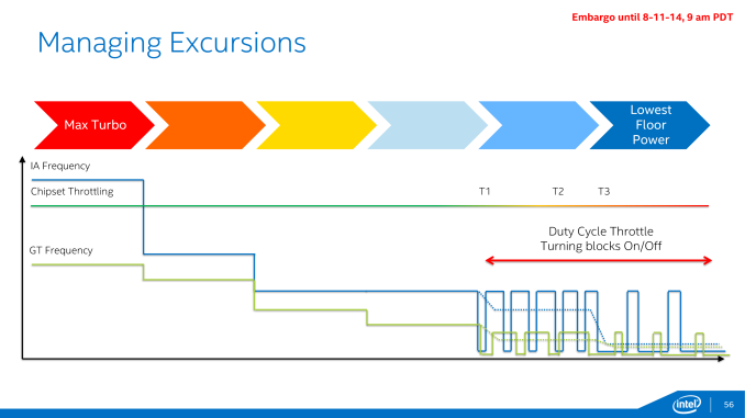
14nm isn’t the only technique Intel has to optimize power consumption on Broadwell’s GPU, which brings us to Broadwell’s final GPU technology improvement: Duty Cycle Control. While Intel has been able to clamp down on GPU idle power consumption over the years, they are increasingly fighting the laws of physics in extracting more idle power gains. At this point Intel can significantly scale down the frequency and operating voltage of their GPU, but past a point this offers diminishing returns. Transistors require a minimum voltage to operate – the threshold voltage – which means that after a certain point Intel can no longer scale down their voltage (and hence idle power consumption) further.
Intel’s solution to this problem is both a bit brute force and a bit genius, and is definitely unlike anything else we’ve seen on PC GPUs thus far. Since Intel can’t reduce their idle voltage they are going to start outright turning off the GPU instead; the process of duty cycling. By putting the GPU on a duty cycle Intel can run the GPU for just a fraction of the time – down to 12.5% of the time – which gets around the threshold voltage issue entirely.
This duty cycling is transparent to applications and the end user, with the display controller decoupled from the GPU clock domain and always staying online so that attached displays are always being fed regardless of what the GPU itself is doing. Control of the duty cycle is then handled through a combination of the GPU hardware and Intel’s graphics drivers, so both components will play a part in establishing the cycle.
Because today’s preview is Broadwell-Y centric, it’s unclear whether GPU duty cycle control is just a Broadwell-Y feature or whether it will be enabled in additional Broadwell products. Like many of Intel’s announced optimizations for Broadwell, duty cycle control is especially important for the TDP and battery life constrained Y SKU, but ultimately all mobile SKUs would stand to benefit from this feature. So it will be interesting to see just how widely it is enabled.
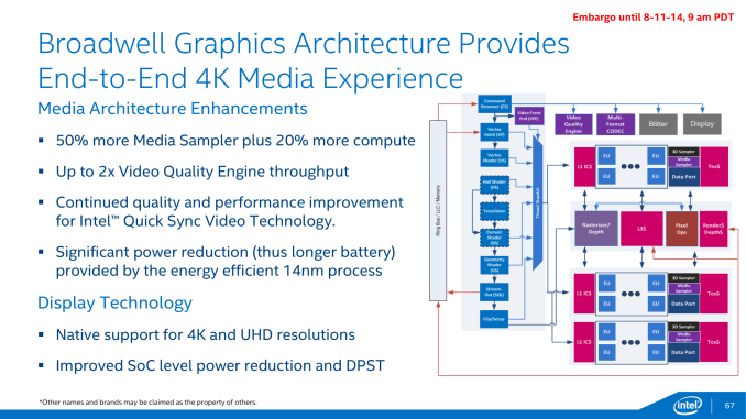
Moving on, last but not least in our GPU discussion, Intel is also upgrading their GPU’s media capabilities for Broadwell. The aforementioned increase in sub-slices and the resulting increase in samplers will have a direct impact on the GPU’s video processing capabilities – the Video Quality Engine and QuickSync – further increasing the throughput of each of them, up to 2x in the case of the video engine. Intel is also promising quality improvements in QuickSync, though they haven’t specified whether this is from technical improvements to the encoder or having more GPU resources to work with.
Broadwell’s video decode capabilities will also be increasing compared to Haswell. On top of Intel’s existing codec support, Broadwell will be implementing a hybrid H.265 decoder, allowing Broadwell to decode the next-generation video codec in hardware, but not with the same degree of power efficiency as H.264 today. In this hybrid setup Intel will be utilizing both portions of their fixed function video decoder and executing decoding steps on their shaders in order to offer complete H.265 decoding. The use of the shaders for part of the decoding process is less power efficient than doing everything in fixed function hardware but it’s better than the even less optimal CPU.
The use of a hybrid approach is essentially a stop-gap solution to the problem – the lead time on the finalization of H.265 would leave little time to develop a fixed function encoder for anyone with a long product cycle like Intel – and we expect that future generation products will have a full fixed function decoder. In the meantime Intel will be in the company of other GPU manufacturers such as NVIDIA, who is using a similar hybrid approach for H.265 on their Maxwell architecture.
Finally, Broadwell’s display controller will be receiving an update of its own. Broadwell is too soon for HDMI 2.0 or DisplayPort 2.0 – it will support HDMI 1.4 and DP 1.2/eDP 1.3a respectively – but the Y SKU in particular is getting native support for 4K. This is admittedly something of a backport since Haswell already supports 4K displays, but in Haswell’s case that feature was not available on Haswell-Y, so this is the first time native 4K support has come to a Y series SKU. This means that Broadwell-Y will be able to drive 4K displays, whether that means a 4K display in the device itself, or a 4K display hooked up internally (with an overall limit of 2 displays on Broadwell-Y). Don’t expect Broadwell-Y to have the performance necessary to do intensive rendering at this resolution, but for desktop work and video playback this should be enough.
Putting It All Together: Low Power Core M
So far we’ve discussed Broadwell’s architecture on a broad basis, focusing on features and optimizations that are fundamental to the architecture. However to talk about the Broadwell architecture is not enough to fully explain the Core M itself. Though many of Core M’s improvements do come from Broadwell, Intel has also made a number of alterations to everything from the CPU packaging to the process node itself specifically for Core M. It’s the resulting combination of these factors that has allowed Intel to iterate on Broadwell-Y over Haswell-Y, and why Intel is so confident in Broadwell-Y’s capabilities and suitability for mobile form factors.
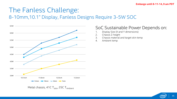
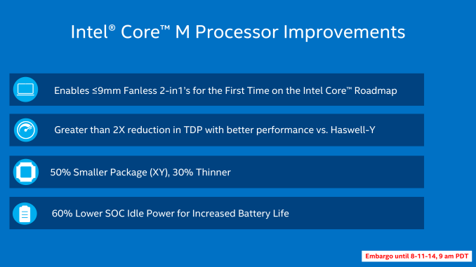
When it comes to building and configuring Core M, Intel likes to refer to their efforts as the “Fanless Challenge,” reflecting the fact that their biggest goal with Core M is to comfortably get the processor in to 10” tablets under 10mm in thickness that are passively cooled. A big part of getting into such a device is meeting the heat dissipation limitations of the form factor – a 10” tablet under 10mm would require a sub-5W SoC – which is where a lot of Intel’s engineering efforts have gone. Broadwell’s performance optimizations, the GPU optimizations, GPU duty cycling, and the 14nm process all contribute to getting a Core CPU’s power consumption down to that level.
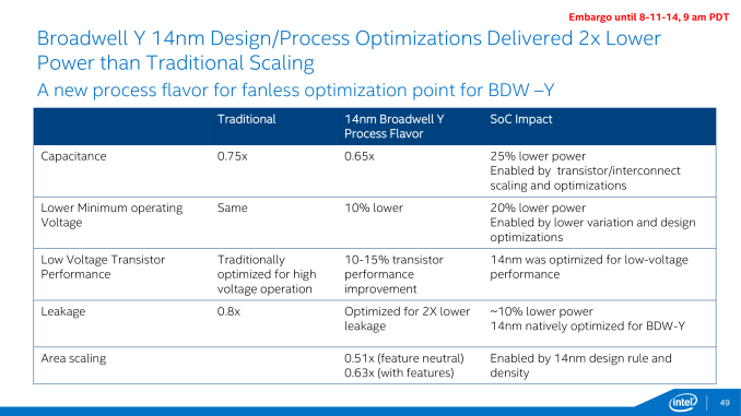
But even that’s still not enough, and for Core M Intel went so far as to give Broadwell-Y its own die and design a low-power optimized version of their 14nm process just for it. This variant is designed to further reduce power consumption by optimizing the resulting transistors for lower power, lower voltage, lower clockspeed operation. By doing this Intel was able to further reduce power consumption in all of the major areas over what would be a traditional 14nm Intel process.
In the resulting 14nm Broadwell-Y process, voltage, capacitance, and leakage were all improved over the traditional 14nm process. Capacitance was reduced by 15%, minimum operating voltages by 10%, and leakage was improved to the point that it reduced SoC power consumption by 10%. The combination of all of these factors serves to significantly lower power consumption over what Intel’s traditional 14nm process would provide.
Working in concert with Broadwell-Y’s 14nm process, Intel has made a number of other changes to further reduce power consumption. Some of these are reflected in Broadwell’s overall design and others are unique to Broadwell-Y, such as using a lower TjMax for Broadwell-Y. By reducing the maximum operating temperature of the chip Intel has been able to realize further power savings by further reducing voltage and decreasing the maximum amount of temperature-dependent leakage the SoC will experience.
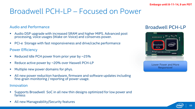
Meanwhile Broadwell-Y’s partner in crime, the on-package PCH, has received its own optimizations to reduce power consumption on the SoC’s total power consumption. The PCH itself is not much of a power hog in the first place – it’s still made on Intel’s 32nm process for this and cost reasons – but with such a strong focus on power consumption every watt ends up counting. As a result the Broadwell PCH-LP has seen optimizations that cut its idle power consumption by 25% and its active power consumption by 20%. Further improvements to the PCH’s monitoring hardware also mean it’s more responsive and can be controlled to a finer degree than the Haswell PCH-LP, and Intel has upgraded to a faster audio DSP to improve performance and reduce power consumption there as well.
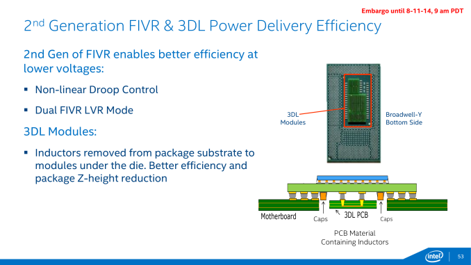
Feeding all of that silicon in turn is Intel’s second generation Fully Integrated Voltage Regulator (FIVR), which further builds off of Intel’s other optimizations. The 2nd gen FIVR has been tuned for Broadwell-Y’s lower voltages, making the FIVR itself more efficient when delivering power at those voltages. To accomplish this Intel has implemented non-linear vDroop control, which is designed to better control the voltage when workload changes would cause voltage overshoots that waste power. And when even the 2nd gen FIVR isn’t efficient enough, this latest FIVR offers a second mode (LVR Mode) for low voltage/workload situations where the FIVR can be partially bypassed to reduce the FIVR’s power consumption.
Interestingly Broadwell-Y also sees the voltage regulation inductors redesigned and relocated in both the name of power efficiency and space efficiency. We’ll get to the case of space efficiency in a moment, but for power efficiency the new 3D inductors (3DLs) have been placed on the underside of the package, allowing the use of more efficient inductors that waste less power.
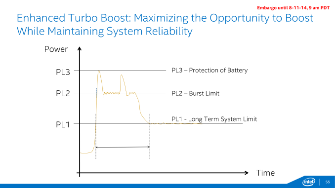
This brings us to the final element of Intel’s power optimization efforts, which involve further adjustments to turbo boost as part of Intel’s “hurry up and go to sleep” motto. New for Broadwell-Y is a 3rd power state, PL3, which allows for even greater turbo boosting, but for only a very limited period of time – on the order of milliseconds. PL3 represents the maximum amount of power the device battery can deliver, and while it’s okay to reach this value sparingly, PL3 is a fast drain that is very hard on the battery. The existence of PL3 in this case is as much for battery protection as it is for performance; it allows devices to tap into PL3 power levels on occasion, all the while allowing PL2 (the regular burst limit) to be defined at a safer value below the battery’s limit. Put another way, by knowing PL3 devices know how to stay farther away from it, which in the long run is what’s best for battery reliability.
Putting It All Together: Small Core M
Next to power constraints, the final element of Intel’s fanless challenge is the size of the SoC itself. Sub-10mm thickness doesn’t just put constraints on the heat capacity of the device but it also constrains just how large an SoC and its supporting circuitry can be. As a result Intel has focused on making Broadwell-Y the smallest Core processor yet, making the entire SoC under 500mm2 in size.
As was the case with power, reducing the size of Broadwell-Y is a multi-faceted effort. The 14nm process plays a big part here, allowing for one of the smallest Core CPU dice yet. At 82mm2 the Broadwell-Y CPU die is some 37% smaller than the Haswell-Y CPU die, none the less packing a dual-core CPU and a full GPU slice.
With such a small die Intel was in turn able to reduce the size of the entire SoC package through the combination of the reduced die area and further optimizations to the packaging itself. Haswell-Y’s already small ball pitch of .65mm was further reduced to just .5mm, producing a package with Intel’s smallest solder ball pads yet. Intel considers the reduction in the ball pitch to be the key change that allowed Broadwell-Y to be so small, as they were already pad-limited on Haswell-Y despite having ample excess packaging even after taking the CPU die’s larger size into account. As a result Broadwell-Y takes up almost 50% less surface area (XY) than Haswell-Y.
Intel has also made a number of changes for Broadwell-Y to reduce the Z-height of the Y SoCs, as even 1.5mm for the SoC starts to become a significant design constraint in a sub-10mm device. Again owing to the 14nm process, the Z-height of the Broadwell-Y die itself is down to 170um. Meanwhile the Z-height of the substrate has been cut in half from 400um to 200um, which accounts for nearly half of the total reduction in SoC Z-height.
The final element in reducing the SoC Z-height, and what’s likely the most unorthodox change for Broadwell-Y’s packaging, is Intel’s 3DL inductors. The 3DLs aren’t just to improve energy efficiency as we discussed before, but they are part of Intel’s efforts to reduce the SoC size. For Broadwell-Y the 3DLs are on their own PCB on the back of the SoC, extending well below the back of the package. To accommodate this, logic boards housing Broadwell-Y will have a hole in them where the 3DL PCB would be in order to allow the complete SoC to fit. Because there are no BGA connections here this change isn’t quite as radical as it first appears, but it’s a very good example of just what lengths Intel was willing to go to reduce the package Z-height.
All told then, the combination of these space optimizations has reduced Broadwell-Y’s Z-height by nearly 30%, from 1.5mm on Haswell-Y to 1.04mm on Broadwell-Y (3DL PCB not included). By bringing Broadwell-Y’s thickness under 1.1mm, the SoC is now no taller than the other common components on a logic board (e.g. RAM), meaning the SoC will no longer stick out above the other components, which is useful both for saving space and for allowing simpler (flatter) heatsinks.
Finally, the smaller size of the Broadwell-Y package will also have a knock-on effect on the size of the logic board, further feeding into Intel’s goals to get Broadwell-Y into smaller devices. Intel tells us that the size of a complete platform (logic) board for Broadwell-Y has been reduced by roughly 25% as compared to Haswell-Y, allowing Broadwell-Y to better fit into not just thinner devices but overall smaller devices too.
Closing Thoughts
Wrapping up our preview of the Broadwell architecture and Intel’s Core M processor, the bulk of Intel’s presentation and focus today is on the latter, so that is where we’ll start.
Core M is not a make-or-break product for Intel, but none the less it is a very important one. Mobile devices – be it tablets, slates, transformers, 2-in-1s etc – are continuing to increase in popularity, and as we’ve seen with ARM based tablets so far they form a market that has continued to grow and continued to erode the x86 laptop market that Intel has dominated for so long. Though laptops as a category are not going anywhere any time soon, their erosion means that Intel needs to get into mobile devices if they want to maintain their sales and their stature. To that end it’s not too late for Intel to break into this market and turn things around, but if they’re going to succeed then they need to make their move sooner or later, and this is where Core M fits in.
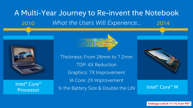
It’s telling then that while Intel is going after this market with a Core architecture, they are doing so under a different Core brand. Core M doesn’t just represent a new low powered Core CPU, but in Intel’s eyes is another product entirely. One that is so different that it does away with the Core i3/i5/i7 convention entirely and gets its own brand name and own product numbers. Core M is still Core, but it is nearly unrecognizable compared to the Core of even 4 years ago.
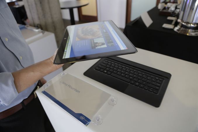
As far as the Core M product is concerned then, while Intel’s plans are grand they are not without merit. Backed by Intel’s new 14nm process and the Broadwell architecture, Core M looks like it should finally resolve the issues that dogged even Haswell-Y by bringing down power consumption even further while improving on Intel’s already strong performance, and getting the resulting processor in an SoC small enough to be usable in even the thinnest mobile devices. In fact from a technical perspective there’s little reason to doubt Core M; we’ll still have to wait to see just how good the resulting retail products are, but there shouldn’t be any technical reason for why it can’t be put into a mobile device comparable to today’s 10”+ tablets. Intel’s own Llama Mountain reference design can vouch for that much, showcasing the viability of Core M in a 12.5” tablet that’s just 7.2mm thick.
Intel's Llama Mountain, a Core M form factor reference design
More likely what will determine Core M’s fate and Intel’s ability to completely break into the mobile device market will be pricing. Intel’s profit margins are somewhat legendary in the computer industry, and a big part of that profitability has come from the high prices Intel has enjoyed from products such as their Core processors. Core M, like the other Cores before it, will still be an upscale product – a higher priced, higher performance alternative to Intel’s mass-market Atom processors. And while that makes plenty of sense on paper, in the real world Intel has to face the AllWinners and other ARM vendors of the world who are happy to sell their ARM SoCs at significantly lower margins, which can have a knock-on effect even if they can’t compete with Intel on overall performance. At this point it’s far too early to call this, especially when Intel isn’t even discussing Core M pricing at this time, but it’s a subject that Intel will have to consider carefully as “good enough” ARM devices will continue to be the biggest threat to Intel’s position in the CPU market.
Moving on, while today’s release from Intel only offers us a preview of what Intel will be delivering with their Broadwell architecture, what Intel has presented thus far looks to continue Intel’s tradition of relentless execution. As a tick Broadwell is a small but respectable improvement in Intel’s Core architecture, with the expected 5% IPC improvement in-line with previous ticks. For more traditional desktops and laptops it won’t radically change the world, but then it never was meant to. The biggest question for these parts will be whether Broadwell will improve on Haswell’s clockspeeds at all – a clockspeed boost made possible by Intel’s 14nm process – or if we’re going to hold steady similar to what we saw with the last tick, Ivy Bridge.
Meanwhile Broadwell’s GPU improvements are more significant, and in the race to further improve what’s essentially the baseline for PC GPU performance it is always welcome. Furthermore the fact that Intel is now at API feature parity with discrete GPUs is a big deal for Intel and it is a big deal for iGPUs as a whole. What we still want to see is more performance; a single slice seems just about right for Core M, but if we’re talking about larger laptop and desktop parts it would be very nice to see something akin to GT3 become baseline, especially with the die size savings Intel will be seeing from the 14nm process.
Finally, from here the rest of Intel’s 2014 should be rather busy. Next month is Intel’s Fall IDF 2014, at which point we expect we’ll be given a deeper look at Broadwell’s architecture. Past that the first Broadwell-Y based Core M processors will be on the shelves for the holidays, and with it our chance to see Broadwell and Intel’s 14nm process in action. However that will also be our only chance to see Broadwell in action this year; while Core M will ship in time for the holidays, the rest of the Broadwell lineup will not appear until 2015.

