Original Link: https://www.anandtech.com/show/7047/the-haswell-ultrabook-review-core-i74500u-tested
The Haswell Ultrabook Review: Core i7-4500U Tested
by Anand Lal Shimpi on June 9, 2013 9:00 AM EST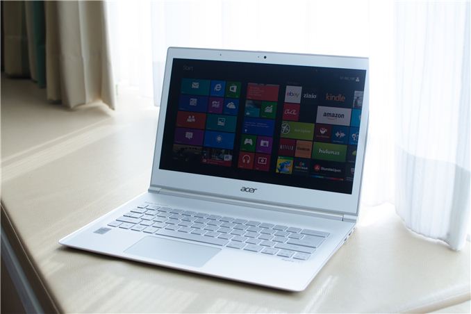
I don’t think I had a good grasp on why Intel’s Haswell launch felt so weird until now. Haswell less than a month after the arrival of a new CEO, and it shows up a couple of weeks after the abrupt change in leadership within the Intel Architecture Group. Dramatic change at the top is always felt several levels below.
To make matters worse, there are now four very important Haswell families that need to be validated, tested, launched and promoted. There’s desktop Haswell, mobile Haswell, ultramobile Haswell ULT (U-series) and Haswell ULX (tablet, Y-series). The number one explanation I’m getting for why we don’t have a socketed K-series SKU with Crystalwell is that everyone is already too busy validating all of the other variants of Haswell that have to launch as soon as possible.
Unlike previous architectures where Intel spanned the gamut of TDPs, Haswell is expected to have success in pretty much all of the segments and as a result, getting everything out on time is very important.
As anyone who has tried to do too much with too little time/resources knows, these types of stories typically don’t end well. The result is one of the more disorganized launches in Intel history and it seems to be caused by dramatic changes at the top of the company combined with a very aggressive to-do list down below.
Haswell is viewed, at least by some within Intel, as a way to slow the bleeding of the PC industry. The shift of consumer dollars to smartphones and tablets instead of notebooks and desktops won’t be reversed, but a good launch here might at least help keep things moving ok until Silvermont, BayTrail and Merrifield can show up and fill the gaps in Intel’s product stack.
| Haswell Ultrabook Requirements | ||
| 2013 Requirement | ||
| Wake | < 3 seconds from S4 sleep | |
| Standby | >= 7 days standby with fresh data (Connected Standby or Intel Smart Connect) | |
| Idle Battery Life | >= 9 hours Windows idle | |
| Video Playback | >= 6 hours HD Video Playback (1080p local video) | |
| Software | Anti-virus, Anti-malware (Win 8 Defender is ok), Intel anti-theft protection & identity theft protection | |
| Networking | 2x2 802.11n minimum + Intel WiDi | |
| Voice | Voice Command/Control Hardware Ready (dual-array microphone baseline) | |
| Display | Touch screen | |
| Thickness |
< 23mm for 14" and above < 20mm 13.3" and below (convertibles include the thickness of both pieces) |
|
| Storage | 16GB of Solid State Storage minimum, 16K PCMark Vantage Score, 80MB/s sequential transfer | |
So Haswell is important, Intel management is in a state of flux, and there’s a lot of Haswell to bring to market. The result? We get a staggered launch, with only some parts ready to go immediately. Interestingly enough, it’s the high-end Haswell desktop parts that are most ready at this point. The stakes are high enough that we had to resort to testing a customer reference platform in order to evaluate Intel’s new Iris Pro graphics. And today, we had to track down a pre-production Haswell Ultrabook in Taiwan to even be able to bring you this review of Haswell ULT.
I’ve spent the past few days in Taipei hunting for bandwidth, running tests in my hotel room and trying my best to understand all there is to know about Haswell ULT, the third Haswell I outlined in our microarchitecture piece last year.
On-Package PCH, The First Single Chip Haswell
In 2010, with Clarkdale and Arrandale, Intel went from a 3-chip platform solution (CPU, IOH/MCH, ICH) down to a 2-chip platform (CPU + PCH). With Haswell, we see the first instantiation of a single-chip Core platform.
With the 8-series chipset, Intel moved from a 65nm process on the 7-series chipset to 32nm, skipping 45nm entirely. An older, less mobile-focused Intel would try to keep its chipsets on the oldest, economically sensible node possible, but these days things are different. The move to 32nm cuts TDP down considerably. Intel hasn’t publicly documented the power consumption any of its ultra mobile chipsets, but if we look at QM77 to QM87 we see a 34% decrease in TDP.
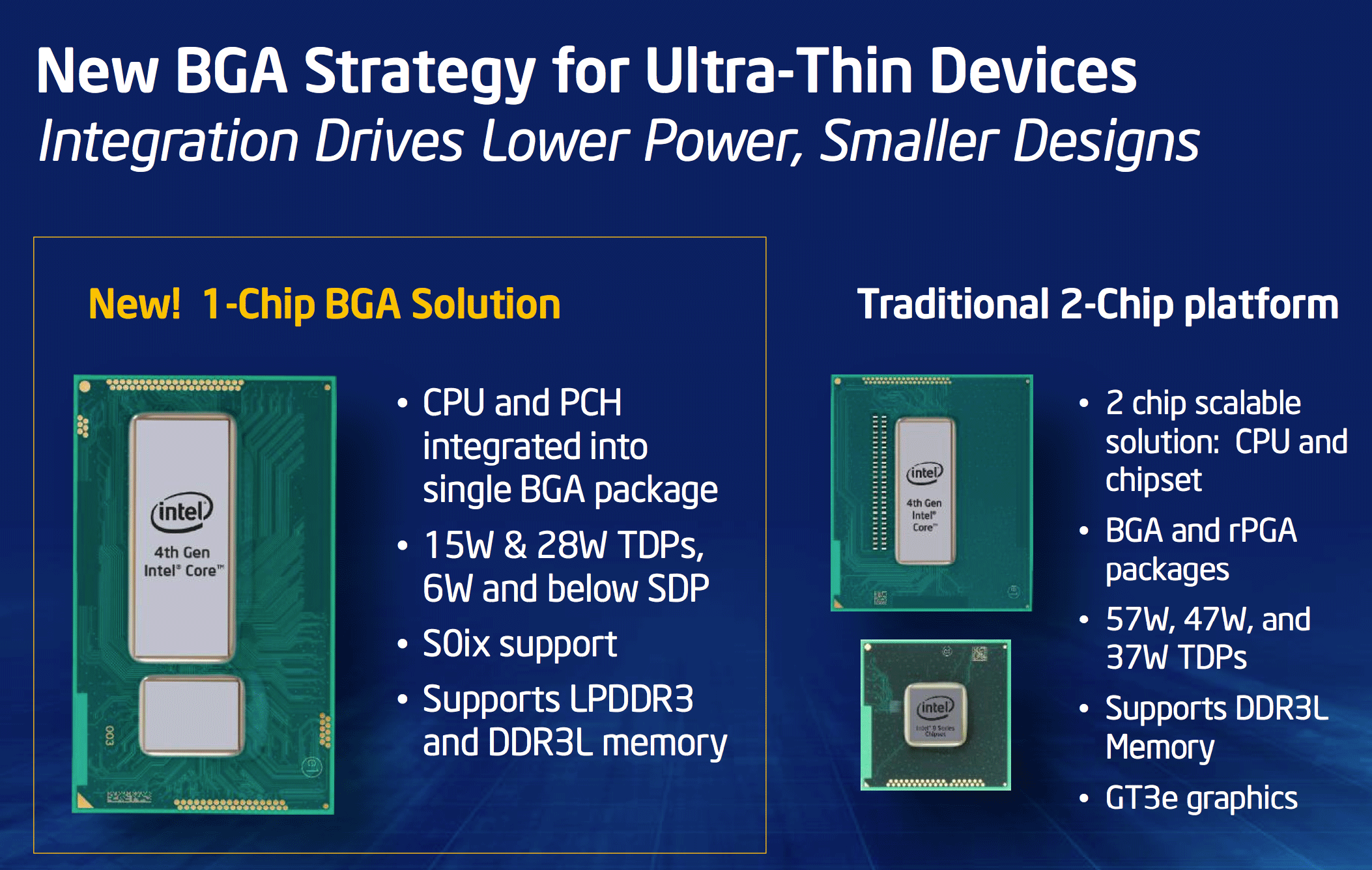
In Haswell desktop and standard voltage mobile parts, the 8-series chipset remains a an off-chip solution in a discrete package. With Haswell ULT and ULX (U and Y series SKUs), the 8-series PCH (Platform Controller Hub) moves on-package. Since it’s on-package, the TDP of the PCH is included in the overall TDP of the processor.
Bringing the PCH on-package not only saves space on the motherboard, but it also reduces the power needed to communicate with the chip. Signals no longer have to travel off die, through the package, via traces on the motherboard to the PCH. Instead you get much lower power on-package communication.
Intel also changed the interface between the CPU and PCH to a new on-package interface instead of DMI. Presumably Intel’s OPI is designed for much lower power operation.
Although PCIe support remains on the PCH (6 PCIe 2.0 lanes), there’s no external PCIe interface from the CPU itself. Any hopes for pairing a meaningfully high performance discrete GPU with Haswell ULT are dead. We didn’t see a ton of Ivy Bridge Ultrabooks with discrete GPUs, but the option simply won’t exist this time around. All of the sudden the creation of Intel’s 28W Haswell ULT with GT3 graphics makes a lot more sense. Haswell ULT lacks native VGA support. Update: NVIDIA tells me that it fully supports running a dGPU off of a x4 connection to the PCH. It's not the ideal solution, but discrete GPUs will still technically be possible with Haswell ULT.
Intel adds SDIO support. USB 3 and 6Gbps SATA are both there as well (although with fewer max ports supported compared to the desktop PCH, up to 4 and 3 respectively). There’s also a lot more sharing of bandwidth between individual PCIe lanes and USB/SATA. These limits shouldn’t be an issue given the port/drive configuration of most Ultrabooks.
Haswell ULT: Platform Power Improvements
Over the past several years, Intel’s maniacal focus on reducing CPU power almost entirely ignored the rest of the platform. Even its own chipsets were often on high power process nodes (remember the first Atom’s 2.5W TDP, but with a 6W chipset TDP). This all changes with Haswell, at least with the ULT/ULX flavors.
I already went through the chipset/PCH changes. The move to 32nm and bringing the PCH on-package will help with power tremendously. But with Haswell, Intel looked beyond its own silicon to other controllers on the motherboard for opportunistic power savings.
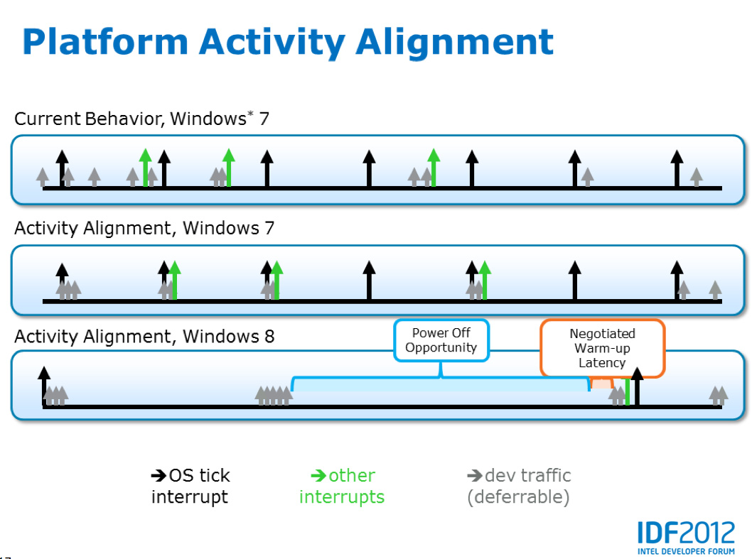
With Haswell, Intel deploys its new platform power management framework called Power Optimizer. Its goal? To deliver S3 (suspend to RAM) style power savings, at S0 (active) style latency.
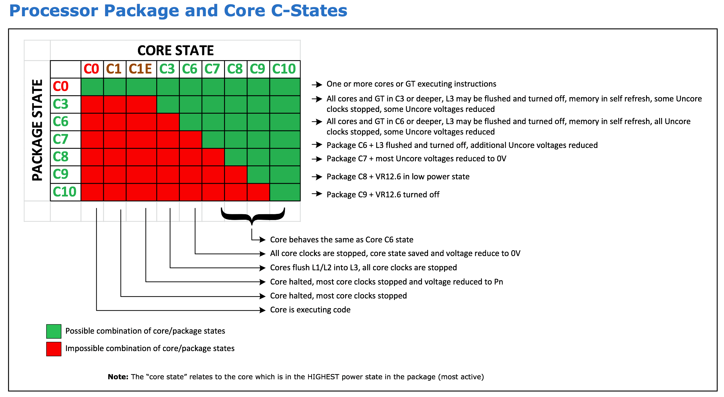
On the CPU, Intel had to dramatically increase its ability to turn blocks on/off, as well as quickly enter/exit its own low power states. Haswell’s FIVR (Fully Integrated Voltage Regular) helps tremendously in this regard as it can quickly switch between voltage states (Intel claims 5x - 10x faster than off-package VR). Haswell as a result can more aggressively choose to go down to lower power states because it can come out of them very quickly. Haswell ULT/ULX support lower core and package C-states. The entire SoC can now be power gated in C10, where the rail that feeds FIVR can be shut off.
For the rest of the platform though, Intel did what the PC industry is best known for: designing a spec and asking others to implement it.
PCIe, SATA, USB 3, DisplayPort are all touched by Power Optimizer. Devices on these busses can report latency tolerance to the PCH (how long can I sleep without breaking everything), and based on that information the PCH can determine how frequently everything has to wake up to avoid impacting user experience.
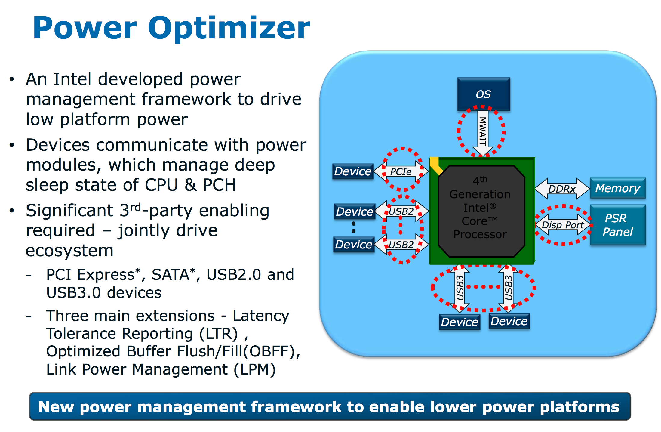
Haswell will take all of the latency tolerance information into account and coordinate system wide sleep/wake based on the least common denominator. The idea is that during idle periods, there’s no reason that most of the platform components can’t be driven down to their lowest power states as if your notebook lid was shut; especially as long as they can quickly wake up when needed. Intel calls this platform level active idle state S0ix, and it’s only supported on Haswell ULT/ULX. In the past Intel had referred to multiple S0ix states, but it looks like Intel is trying to move away from that nomenclature. Effectively now there’s just S0 and S0ix in terms of active power states.
Obviously all it takes is a single 3rd party component to ruin everything, so Intel has worked with device and microcontroller manufacturers to help improve their power profiles as well. Intel’s Power Optimizer architecture is very robust. Intel plans on working with platform vendors regularly to improve power. There are no more easy power gains; going forward, reducing power is going to require a much more collaborative effort from all the power consumers on the platform.
Windows 8 also plays a significant role in all of this as the OS supports coalescing of tasks in software to ensure that it isn’t working against Intel’s Power Optimizer in hardware.
If the CPU/SoC and much of the motherboard can aggressively drive down to S3-like idle power, the display becomes an even bigger burden than it has in the past. To allow the entire platform to go to sleep while the display is still active, Intel recommends Panel Self Refresh (PSR) to be implemented in Haswell Ultrabooks. The idea behind PSR is to put DRAM on the panel itself to store the frame buffer. In the event of a static display (e.g. staring at a Word document, looking at your desktop), the GPU frame buffer is copied to the panel’s DRAM, and the GPU itself is shut off instead of having to drive meaningless content updates to the display 60 times per second. With PSR, the SoC can go into its deepest sleep state (C10).
No Connected Standby for Now
Although you should be able to realize some of the benefits from S0ix with the first Haswell Ultrabooks, Connected Standby (periodic content refresh while in a sleep state) requires OS support. For Haswell Ultrabooks, that means waiting for Windows 8.1.
Even on the S0ix side, it’s not clear to me whether all of the devices in the system capable of going into D3 (their lowest power state) while active will actually do so until Windows 8.1. I get the distinct impression that Haswell Ultrabooks will see a tangible increase in battery life with Windows 8.1.
Haswell ULT Graphics
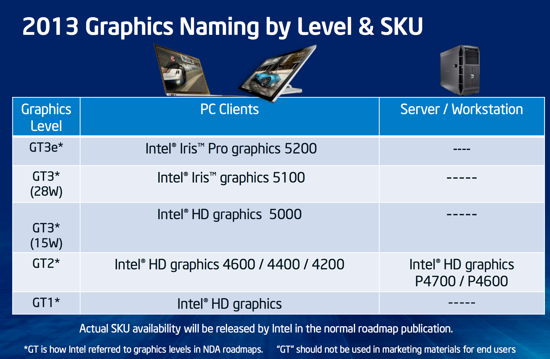
As I mentioned in our Iris Pro review, Intel’s 128MB eDRAM die (codename Crystalwell) isn’t available on any dual-core parts, excluding it from Haswell ULT. Intel will offer both GT2 and GT3 GPU (20EU/40EU) implementations however. With max GPU clocks below 1100MHz, these parts are devoid of Iris Pro branding and are instead referred to as Intel HD Graphics.
The Test System and Haswell ULT SKUs
Before Computex, Acer announced the 2nd generation Aspire S7 based on Haswell ULT. I managed to get my hands on an early version of the new S7 and that will serve as the platform for the performance and battery life comparisons going forward.
I’ll do a separate piece, likely post-Computex, on the new S7 but I did want to share some preliminary thoughts about the machine here. The 2nd generation S7 looks a lot like the Ivy Bridge model. The chassis retains the Gorilla Glass covered display backing, aluminum base and capacitive touch screen. The Aspire S7 is still a beautiful notebook and shows huge progress from where Acer was just a few years ago. Despite the similarities, the 2nd generation Aspire S7 does come with some much needed tweaks and enhancements.
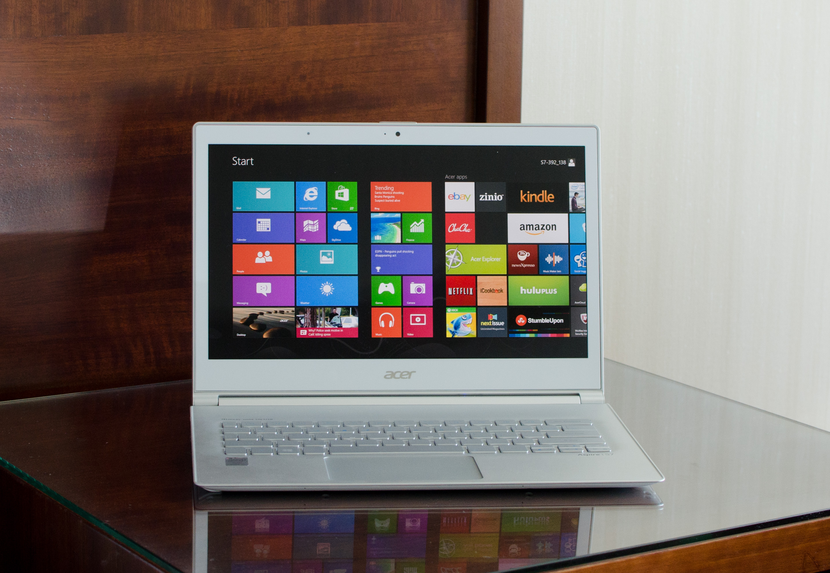
Acer started with the backlit keyboard, and increased key travel almost to the point of the MacBook Air. I didn’t have a ton of experience with the previous generation model, but this one feels a millimeter or so short of the travel on the MacBook Pro with Retina Display. Unfortunately there’s still no function lock, which means that things like Alt+F4 are still three-key combinations. The clickpad is powered by Elan, although I’ve heard murmurings of Acer switching to Synaptics going forward. Synaptics remains the closest to providing an Apple-like solution for clickpad performance, although even its solutions still need a little more work. Ergonomically the S7’s clickpad is recessed into the chassis just slightly more than I’d like.
The display was the target of major attention as well. By default the new Aspire S7 comes with a 13.3-inch 1920 x 1080 panel, however some models will offer an optional 2560 x 1440 panel instead. Unfortunately my sample only had the 1080p panel, but I’ve seen the 1440p version up close and it’s very impressive. I’m glad to see more PC notebook vendors not only go beyond 1366 x 768, but also exceed 1080p. Now all we need is for Microsoft to do a better job of handling high-DPI monitors in desktop mode.

Internally, my sample has a Core i7-4500U. The 4500U is the spiritual successor to the Core i7-3517U from our 1st generation Aspire S7 review unit. A look at the high level specs points to only a 100MHz reduction in base frequency, but identical max turbo frequencies. On the GPU side, there’s an increase in the number of EUs but relatively similar max operating frequencies. Based on the EU and clock differences, the max increase in graphics performance should be limited to around 19.5% (assuming both Haswell and Ivy Bridge are capable of hitting the same GPU turbo frequencies with the same regularity). I’m very eager to get my hands on an Ultrabook based on Intel’s GT3/HD 5000/Iris 5100, however that will have to wait for another day.
| Intel 4th Gen Core i7/i5/i3 Dual-Core U-Series Processors | ||||||||
| Model | Core i7-4650U | Core i7-4550U | Core i7-4500U | Core i5-4350U | Core i5-4250U | Core i5-4200U | Core i3-4100U | Core i3-4000U |
| Cores/Threads | 2/4 | 2/4 | 2/4 | 2/4 | 2/4 | 2/4 | 2/4 | 2/4 |
| CPU Base Freq | 1.7 | 1.5 | 1.8 | 1.4 | 1.3 | 1.6 | 1.8 | 1.7 |
| Max SC Turbo | 3.3 | 3.0 | 3.0 | 2.9 | 2.6 | 2.6 | n/a | n/a |
| Max DC Turbo | 2.9 | 2.7 | 2.7 | 2.6 | 2.3 | 2.3 | n/a | n/a |
| TDP | 15W | 15W | 15W | 15W | 15W | 15W | 15W | 15W |
| HD Graphics | 5000 | 5000 | 4400 | 5000 | 5000 | 4400 | 4400 | 4400 |
| GPU Clock | 200-1100 | 200-1100 | 200-1100 | 200-1100 | 200-1000 | 200-1000 | 200-1000 | 200-1000 |
| L3 Cache | 4MB | 4MB | 4MB | 3MB | 3MB | 3MB | 3MB | 3MB |
| DDR3/DDR3L | 1600 | 1600 | 1600 | 1600 | 1600 | 1600 | 1600 | 1600 |
| vPro/TXT | Yes | No | No | Yes | No | No | No | No |
| VT-d | Yes | Yes | No | Yes | Yes | No | Yes | Yes |
| Intel SBA | Yes | Yes | Yes | Yes | Yes | Yes | ||
Like all 15W Ultrabooks, the Aspire S7 uses a single fan to cool the Haswell CPU. You will hear the fan ramp up, and the bottom of the chassis gets warm, but neither were uncomfortable to me personally.
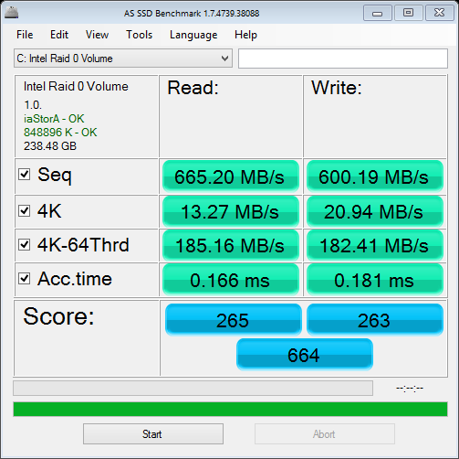
Acer continues to use an internal RAID-0 of Lite On mSATA SSDs. In this case there are two Marvell 88SS9174 based SSDs in RAID-0. The combination yields a peak sequential throughput of 665MB/s, which is pretty fast for an Ultrabook. Although I’d personally prefer a simpler, non-RAID setup, I can understand why Acer would be tempted to do something like this.
The SSDs in the S7 now support device sleep (DEVSLP), which boasts incredibly low power consumption when the system is asleep. The way it works is pretty neat. Using HIPM and DIPM, SSD controllers can do a good job of powering down big blocks of the controller however the SATA PHY can’t be powered down otherwise you risk losing communication with the drive itself. The device sleep spec calls for an out of band signal telling the SSD when it can go to sleep and when it can wake up. Since the signal is out of band, the SATA PHY doesn’t need to be active for communication, and thus the SATA PHY itself can power down. Lite On tells me that in DEVSLP mode, its SSDs will draw somewhere around 2mW of power - that’s compared to around 100mW when they’re in DIPM slumber. With Haswell, Intel is very focused on driving power outside of the CPU as low as possible - DEVSLP is a very good example of doing just that.
Acer dramatically increased the battery capacity of the Aspire S7 from 35Wh up to 46Wh. Despite the higher capacity battery there’s no increase in weight. The 13.3-inch S7 still weighs around 2.86 lbs.
Battery Life
I didn’t get my hands on the Haswell S7 until a few hours after I landed in Taipei. My hotel’s in-room internet was throttled to around 2.5Mbps, which wasn’t enough bandwidth to reliably run our web browsing battery life tests. Luckily, I had my review copy of PCMark 8 on hand with its new built in battery life tests. I asked Jarred to run comparison data on the Ivy Bridge S7.
We had time to perform multiple runs on two of the tests: Home and Creative.
From the PCMark 8 Technical Guide:
The PCMark 8 Home benchmark test includes a set of workloads that reflect common tasks and activities performed by a typical person at home. These workloads generally have low computational requirements making the PCMark 8 Home benchmark suitable for testing the performance of low-cost tablets, notebooks and desktops.
The PCMark 8 Home benchmark test contains the following workloads: Web Browsing, Writing, Casual Gaming, Photo Editing and Video Chat.
The PCMark 8 Creative benchmark test includes a set of workloads that reflect tasks and activities typical of more advanced home computer users. With more demanding requirements than the Home benchmark, the PCMark 8 Creative test is suitable for testing the performance of mid-range computer systems. Your system must have a GPU with full DirectX 11 support in order to run all the workloads in the PCMark 8 Creative benchmark.
The PCMark 8 Creative benchmark test contains the following workloads: Web Browsing, Photo Editing, Batch Photo Editing, Video Editing, Media to Go, Mainstream Gaming and Group Video Chat.
As always, I calibrated both displays to the same brightness (200 nits). In the case of the Haswell based S7, I disabled all additional display power saving options in the Intel driver. Keeping in mind the new S7 has a 33% larger battery, I’m presenting both absolute battery life numbers as well as minutes per Wh for normalized comparisons.
The PCMark 8 Home battery life test is the lighter of the two, and thus has the best chance of showing peak improvement on Haswell. The results are very good:
| PCMark 8 Battery Life | ||||
| PCMark 8 Home | PCMark 8 Home (Normalized) | PCMark 8 Creative | PCMark 8 Creative (Normalized) | |
| Acer Aspire S7-391 (Core i7-3517U) | 2.83 hours | 4.857 mins/Wh | 3.35 hours | 5.743 mins/Wh |
| Acer Aspire S7-392 (Core i7-4500U) | 5.2 hours | 6.783 mins/Wh | 5.12 hours | 6.674 mins/Wh |
| Haswell Advantage | 39.6% | 16.2% | ||
In both benchmarks, Haswell ULT delivers 11 - 14% better performance and substantially longer battery life. Normalized for battery capacity, Haswell ULT offers 16% better battery life in the Creative test and almost 40% better battery life in the Home test. Note that the performance advantage pretty much disappears once we move to the Balanced power profile with the laptop connected to the wall.
| PCMark 8 Performance | ||||
| PCMark 8 Home (Power Saver) | PCMark 8 Home (Balanced) | PCMark 8 Creative (Power Saver) | PCMark 8 Creative (Balanced) | |
| Acer Aspire S7-391 (Core i7-3517U) | 1595 | 2694 | 1391 | 2508 |
| Acer Aspire S7-392 (Core i7-4500U) | 1777 | 2832 | 1583 | 2553 |
| Haswell Advantage | 11.4% | 5.1% | 13.8% | 1.8% |
Update: I made it back to the US, equipped with decent internet speeds, I was able to run our light 2013 web browsing battery life test. The increase in battery life is tremendous:
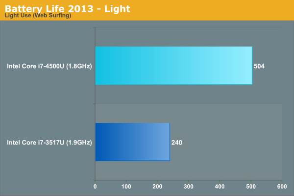
The new S7 delivers over 2x the battery life of the old model. Normalizing for battery capacity, the improvement due to Haswell is 57.5%. These results track perfectly with what we saw in PCMark 8. Workloads with greater idle time will show the biggest improvement in battery life thanks to Haswell ULT.
CPU Performance
With Haswell on the desktop we showed a 0 - 19% increase in performance over Ivy Bridge at the same clocks. With Haswell ULT, similar parts have identical turbo frequencies but Haswell does drop the base clock by 100MHz in this case. There’s also a lower TDP, and that TDP now includes the PCH as well, potentially decreasing the time spent in max turbo.
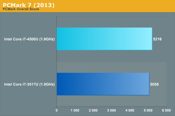
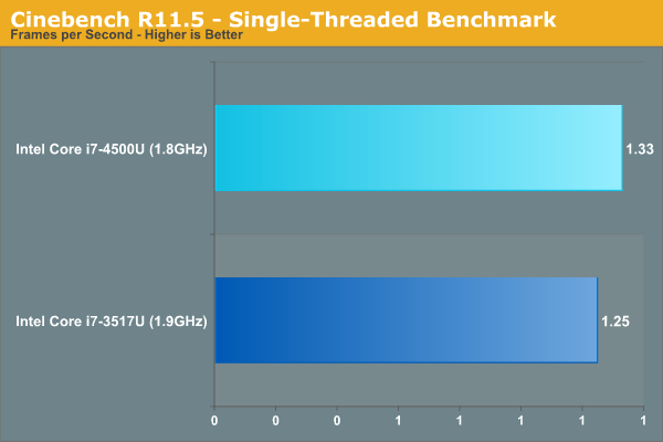
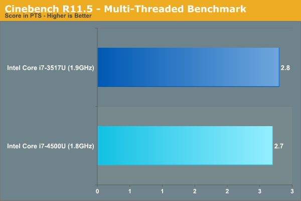
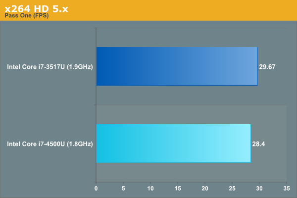
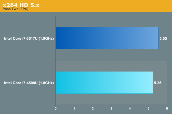
The end result is effectively no gain in performance across our benchmarks. PCMark 7 and single-threaded Cinebench show a 3 - 6% increase in performance, while multithreaded Cinebench and x264 show a 3 - 5% decrease in performance.
As we saw in our battery life tests, it looks like there are some larger performance gains to be had in power limited scenarios. The explanation there makes sense. Haswell ULT’s lower TDP may cap max frequencies more than on Ivy Bridge, but at lower frequencies the CPU cores are less likely to bump into the chip’s TDP limits - allowing Haswell’s IPC advantage to really shine. When plugged in however I wouldn’t expect CPU performance any different from Ivy Bridge.
| CPU Performance Comparison | ||||||||
| PCMark 7 | Cinebench 11.5 (single threaded) | Cinebench 11.5 (multithreaded) | x264 5.0.1 - 1st pass | x264 5.0.1 - 2nd pass | PCMark 8 Home (Power Saver) | PCMark 8 Creative (Power Saver) | ||
| Core i7-3517U | 5058 | 1.25 | 2.8 | 29.67 | 5.55 | 1595 | 1391 | |
| Core i7-4500U | 5216 | 1.33 | 2.7 | 28.4 | 5.25 | 1777 | 1583 | |
| Haswell Advantage | 3.1% | 6.4% | -3.5% | -4.3% | -5.4% | 11.4% | 13.8% | |
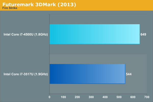
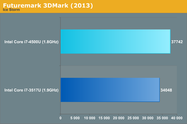
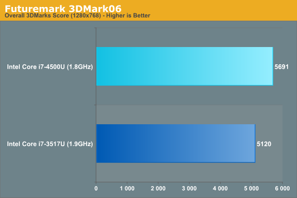
GPU Performance
With a modest increase in EU hardware (20 EUs up from 16 EUs), the Intel HD 4400 GPU in the Core i7-4500U I’m testing today isn’t tremendously faster compared to the HD 4000 in the i7-3517U. On average I measured a 15% increase in the subset of game tests I was able to run in Taipei, and a 13% increase in performance across our 3DMark tests. The peak theoretical increase in performance we should see here (taking into account EU and frequency differences) is 19%, so it doesn’t look like Haswell is memory bandwidth limited just yet.
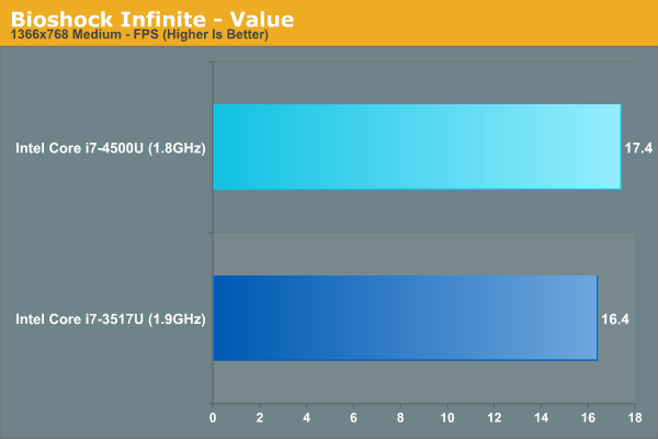
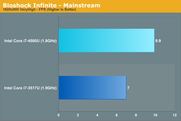

If we throw 35W Trinity into the mix, HD 4400 gets closer but it's still far away from 35W Trinity performance:
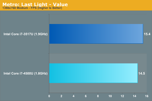
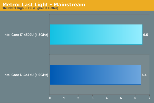
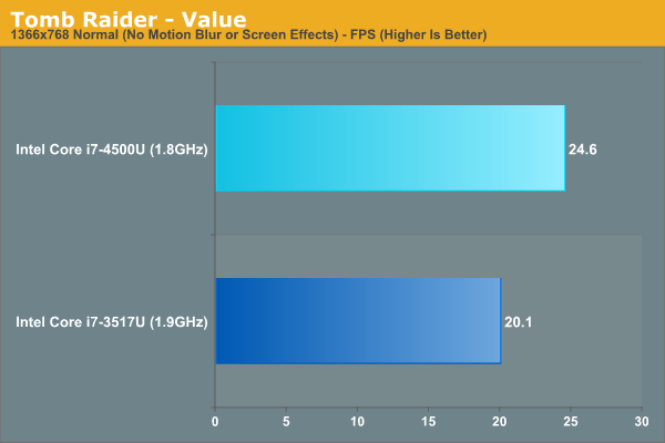
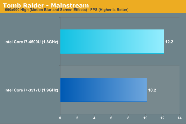
| GPU Performance Comparison | ||||||
| Metro: LL - Value | Metro: LL - Mainstream | BioShock Infinite - Value | BioShock Infinite - Mainstream | Tomb Raider - Value | Tomb Raider - Mainstream | |
| Core i7-3517U | 15.4 fps | 6.0 fps | 16.4 fps | 7.0 fps | 20.1 fps | 10.2 fps |
| Core i7-4500U | 14.5 fps | 6.5 fps | 17.4 fps | 9.9 fps | 24.6 fps | 12.2 fps |
| A10-4600M | 16.8 fps | 8.0 fps | 25.8 fps | 10.0 fps | 30.1 fps | 12.7 fps |
For light gaming, Intel’s HD 4000 was borderline reasonable. Intel’s HD 4400 takes half a step forward, but it doesn't dramatically change the playability of games that HD 4000 couldn't run well. Personally I’m very interested to see how the 28W Iris 5100 based Haswell ULT part fares later this year.
Final Words
On the desktop, Haswell offers a reasonable increase in IPC, and a decrease in idle power consumption. The combination of the two feel very evolutionary over Ivy Bridge however. In high-end notebooks, Iris Pro dramatically improves the processor graphics story by finally delivering discrete GPU class gaming performance. In Ultrabooks, Haswell’s offer is dominated by significant improvements in battery life.
Intel refers to Haswell ULT’s performance in Ultrabooks as being the single largest improvement in battery life of Intel history. As far as I can tell, that’s true. Under heavy load I wouldn’t expect any substantial increase in battery life, however most notebook usage models boast significant periods of idle time. Staring at your screen, browsing the web, or even multitasking all offer opportunities for idle power optimizations to kick in. That’s where Haswell ULT excels. Using Acer’s Aspire S7 as a comparison platform and normalizing for battery capacity differences I measured anywhere from a 15% to a 60% increase in battery life thanks to the move to Haswell.

Peak CPU performance doesn’t really change with Haswell ULT. Performance on battery on the other hand does improve by a bit over 10%. On the GPU side you should expect to see around a 15% increase in performance compared to last generation’s HD 4000 GPU. Neither improvement is significant enough to dramatically change the performance class of Ultrabooks, but the situation at least improves.
With the last generation of Ultrabooks, the tradeoff between portability and battery life was more evident than ever. The Ultrabook targeted Haswell U-SKUs aim to change that. Based on what I’ve seen here, they will.


