Original Link: https://www.anandtech.com/show/700
Integrated Video Chipset Roundup - January 2001
by Matthew Witheiler on January 10, 2001 4:23 AM EST- Posted in
- Motherboards
Lets face it: there are a good number of us out there who are forced to build a PC on a very limited budget. Be it because we are building a second PC simply for recreational use, want a system for the kids, are are simply looking to build a low cost machine, many are faced with the difficult task of building a high performance computer system on a budget.
As recently as a few years ago, attempting to build such a value system would often result in a major disappointment. Many times reducing the cost of a system required stepping back to older technology and products with limited support and very lackluster performance. Luckily, the task of building a budget system is getting easier and easier with the advent of component integration.
The idea of component integration is certainly nothing new. It is quite logical to think that placing many components on a single chip would save cost over many separate chips, power components, PCBs and the like. It was not until rather recently, however, did the technology allowing a high degree of component integration come into realization. Although some see the future as a complete system integrated onto a single square of silicon, we are not quite there yet. Instead, manufacturers of today are attempting to integrate one or two common components onto an already existing chip.
Perhaps the most likely site to find component integration today lies in the north bridge controller of a chipset, a location where it is fairly easy to integrate fairly costly system components. We have seen everything from sound to video integrated in north bridge chips, but the one integration that seems to have caught on is video integration, where a graphics chip is embedded onto an existing north bridge chip.
Normally we are quick to scold integrated video due its poor performance when compared to higher performing, and higher costing, separate video cards. Since every integrated video solution has been implemented to save cost, many times performance is cut as well in order to make the chips easier to produce.
However, rather than quickly brush integrated video solutions off as a nonviable solution, one must first consider the reason for integration: reduced cost. Although a integrated video may not be desirable in a high performance gaming system, it may strike the perfect balance between price and functionality in a value system. But with many integrated solutions currently available, one question remains: which solution is the best? Follow us as AnandTech takes you through the world of integrated video solutions in order to find out which is the right solution for you and your value system.
Integrated Video: How it Works
The north bridge is perhaps the most convenient place to locate many system components, but most of all the video processor. This is due to one of the various functions which the north bridge controls which happens to be the AGP interface.
Since it is the north bridge that controls the interface for the vast majority of video cards out there, it only makes sense that any video integration occurs on this chip. By placing a video processor on the same silicon that controls the signals it gets and sends to the CPU, integrating a video processor on this chip not only makes sense but also reduces the traces and board space necessary to carry information to the offboard AGP graphics controller.
Although it is logical to place the graphics processor on the north bridge, we all know that there is more to a video card than just a processor. Not only must a video card process what it is sent, it must also store this information as well as provide a way to get it to the monitor. There are two different ways to attack the problem of temporary data storage.
The first approach involves placing separate RAM chips on the motherboard itself; in essence, physically soldering the same RAM chips found on current video cards onto the motherboard instead. From there, traces are made from the north bridge with integrated video to this onboard memory, providing a path for the data to travel. The speed of this path is dependent on the width of the path (how many bits it can send in one clock speed, 64-bit in the solutions we are looking at today) as well as the speed the data can travel. The total speed at which information can move from the integrated graphics chip to the external memory is called memory bandwidth and is measured by multiplying the bus width of the memory bus, times the clock speed of the memory, divided by 8 (the number of bits in a bite).
The use of separate SDRAM chips to provide a frame buffer for video storage is called local frame buffer mode and is typically avoided by manufacturers. This is because the addition of 4 to 32 MB of memory on the motherboard increases the base price of the motherboard. Since the goal of most of the integrated video solutions out there is to decrease cost, adding components that dramatically increase the cost of a motherboard are avoided for the most part.
The road more commonly traveled in the integrated video market involves a frame buffer solution called unified memory mode. In a unified memory mode configuration, a systems own memory (RAM) is used as a frame buffer for the video card. A certain amount of system SDRAM is set aside to act solely as the integrated video's frame buffer. Just as in a local frame buffer solution, the speed at which data travels to and from the system memory is dependent on both the bus width and the memory speed. In the case of unified memory solutions, the bus width is always 64-bits wide (for all integrated solutions out there currently, anyway) and the speed is from 100 MHz to 133 MHz, or the speed that the system memory performs at. Although this may sound like the memory bandwidth of this setup would be similar to the memory bandwidth of a local frame buffer solution (since both have a 64-bit bus and typically 133 MHz memory), the memory bandwidth of a shared memory buffer solution actually proves to be much less.
The reason for this is simple. Unlike a local frame buffer solution that has its own path to the frame buffer, unified memory solutions share a path with a computer's bus, a path already crowded as it is. Sharing a path with the same system that is already loaded down by carrying information from the CPU to the system memory and back, the actual memory bandwidth in a unified memory solution is far less than the ideal 1.06GB/s of theoretical bandwidth available in a system with a 133 MHz front side bus.
It is much cheaper to rely on a user's system memory to serve as a frame buffer, as no RAM chips need to be physically added to the motherboard; the system is total dependent on memory added after the sale of the motherboard. For this reason, the vast majority of integrated video systems out there work in shared memory mode, saving production costs but hampering performance.
As for the other parts of a video card, all elements are contained on the motherboard itself. Filters used to provide a clean video signal, as well as the video BIOS and other necessary components, are placed where ever convenient on the motherboard design. The 15-pin VGA port is almost exclusively positioned in the location of one of the two serial ports found on the ATX form factor. This is a convenient location for the port, as both the 15-pin VGA port and the 9-pin serial port are essentially the same size.
Apart from the aforementioned components, many of the items found on a standard video card are actually power regulating components that are not necessary in an integrated solution.
Now that we know a bit about the types of integrated video systems out there as well as how they work, lets review what solutions are currently being offered before we see which one performs best.
Socket-A Solutions: SiS' 730S
We were pleasantly surprised when we recently had a chance to get our hands on SiS' integrated video solution for the Socket-A platform, the SiS 730S chipset. It was the first chipset of its kind to enter the Socket-A market, potentially brining the platform down to lower cost systems.
Despite exceptional performance for the price, AMD's Duron processor was having quite a hard time entering the value PC field. Unlike Intel's Celeron solution, AMD's Duron processor lacked one thing: an integrated motherboard to work with. Without having a low cost motherboard solution out there, the Duron processor was essentially eliminated from the large system manufacturer pool such as Gateway and Compaq. Since from the OEM's perspective, where price is the bottom line, it did not matter that the Duron outperformed Intel's Celeron processor clock for clock, all that mattered is that it cost significantly more to build a Duron computer since an additional video card had to be added to the package. SiS saw the opportunity to bring the Duron processor to the large scale value PC market and the product of this realization is the SiS 730S chipset.
The SiS 730S takes integration to a higher level then previously encountered, incorporating not only the graphic controller but also the south bridge. The SiS 730S uses the SiS 300 graphics core, a solution designed by SiS themselves. Similar to other integrated graphics controllers out there, the SiS 300 graphics core takes integrated performance one step further by incorporating hardware motion compensation and iDCT support. This helps to reduce CPU usage while playing DVD/MPEG2 streams which typically consume a large amount of processing power. More information about these two features can be found in our DVD Quality, Features, and Performance article.
The SiS 300 uses the unified memory architecture described in the "How it Works" section of this review, meaning that the graphics controller makes use of system memory for the frame buffer. Depending on the memory used, PC100 or PC133, the SiS will have a theoretical maximum memory bandwidth of 800MB/s (PC100) or 1.06GB/s (PC133). Once again, the video controller is sharing this bandwidth lots of other data that is normally traveling to and from the system memory, meaning that this maximum memory bandwidth number is never fully realized.
The integration of the south bridge in the north bridge chip is another method SiS took to reduce chipset cost. Not only are the traces between the north bridge and the south bridge eliminated, the board can be physically smaller as there no longer needs to be space for a second physical chip.
The SiS 730S also supports an external AGP 4X port, making upgrade possible. The system can operate with PC133 or PC100 SDRAM memory and offers no support for DDR. Other features include support for 6 USB ports as well as AC'97, integrated ethernet, and Modem Riser card support. One final unique feature of the SiS 730S platform is the fact that the northbridge has a dedicated 133MB/s path to the IDE channel, meaning that any bottlenecks that may arise when ATA/100 drives become mainstream should be solved.
For more information on the SiS 730S chipset, please see our full review of the chipset.
The SiS 730S Reference Board

Socket-A Solutions: VIA's KM133
The second integrated Socket-A solution that we got our hands on was the VIA's KM133, the second of only two integrated Socket-A solutions we have seen to date. Much like SiS is attempting to do with their 730S chipset, VIA is also trying to make the Duron processor more popular in value markets where it has previously been excluded from due to the lack of an inexpensive solution.
The KM133 uses the ProSavage graphics core; a core VIA claims is made up of the Savage4's 3D core and the Savage 2000's 2D core. The decision to use an S3 chip in the KM133 was an easy one for VIA. Ever since VIA acquired S3's graphics division in the summer of 2000, VIA has gained full access to the S3 line of graphics cores so incorporating the ProSavage chip in the KM133's northbridge did not require a completely new core design.
The ProSavage chip uses a unified memory architecture, meaning once again that the frame buffer for the video controller is located in the system memory. Since the board supports both PC100 and PC133 memory, the maximum available memory bandwidth is 800MB/s or 1.06GB/s depending on the memory used.
Besides the addition of the ProSavage graphics controller, the KM133 is identical to the KT133 northbridge. This means that the two share the same memory controller, AGP controller and the like. So, with the addition of an external AGP card that is supported with the external AGP 4X port, the KM133 should perform identically to the KT133.
The board manufacturer has the decision of which south bridge to mate the KM133 with. The most common mate will be either VIA's 686A or 686B chip, with the only difference between the two being the fact that the 686B chip supports ATA/100 while the 686A chip only support ATA/66. Otherwise, both chips feature support for 4 USB ports and AC/MC'97 codecs. The cost of the KM133 is only about a dollar above the cost of SiS' 730S chipset.
For more information on VIA's integrated Socket-A solution, the KM133, please see our VIA KM133 Socket-A Chipset review.
VIA KM133 Reference Board

Socket370 Solutions: Intel's i815
Intel was one of the first to bring integrated video support to the Socket-370 platform with their i810 chipset solution. Luckily, Intel recently launched the i815 as the i810's successor. Since this chipset offers both integrated video support as well as external AGP 4X support, it found its way into many more systems than the original i810 did.
Intel's i815 chipset is one of the more powerful Socket370 solutions out there when matted with an external AGP 4X video card. The chipset was the first Intel made SDRAM chipset to exploit the 133 MHz front side bus speed while still having an external AGP slot, allowing for much faster system performance. Naturally, the i815 also supports 66MHz and 100MHz front side bus speed. In addition, the 801AA I/O controller hub (effectively the south bridge) mated with the i815 supports Ultra ATA 66/33 as well as 2 USB ports and an AMR slot. There is also the 801BA I/O controller hub which supports Ultra ATA/100, integrated ethernet, CNR, and 4 USB ports.
The integrated graphics on the i815 chipset is the same integrated graphics controller used originally in the i810 northbridge. Intel calls this chip their GMCH, standing for the graphics and memory controller hub. At the heart of the GMCH is a graphics controller that is essentially an i740 accelerator. One thing that the i815 looses from the i810 incarnation of this chip is an option for onboard display cache, meaning that a local frame buffer solution is not available for the i815. Instead, the i815 offers two frame buffer solutions.
The first place that the i815 looks for space for a frame buffer is in what Intel calls a Graphics Performance Accelerator (GPA). This is essentially a 4MB display cache placed on a card that is inserted in the 815 motherboard's AGP 4X slot. This allows the GMCH to look for a frame buffer here, where data is able to pass to and from the GPA at the AGP 4X rate of 1.06GB/s. Although it seems like this is the same amount of memory bandwidth offered by a unified memory architecture with PC133 memory, the GPA does not have to compete with additional data passing over the bus. Since no additional data is passing over the AGP bus, GPA can transfer data at the full 1.06GB/s. This provides much more memory bandwidth for the GMCH when reading and writing to the GPA.
4MB is not a lot of frame buffer, however. When the graphics performance accelerator memory runs out, the graphics and memory controller hub turns to the system memory for additional frame buffer space. This means that once again the data must travel over the already busy memory bus, thus decreasing performance when performing read and write operations on the system memory.
For more information on the i815 chipset, please see our Intel i815 Chipset review.

Socket370 Solutions: ALi's Aladdin TNT2
As one may suspect by the name of this Socket370 chipset, ALi's Aladdin TNT2 offers an integrated NVIDIA TNT2 graphics controller on ALi's M1621 northbridge. This northbridge supports bus frequencies of 66, 100, and 133MHz but does not feature support for an external AGP 4X slot. The most common south bridge to be paired with the M1621 northbridge is ALI's M1535D which features support for up to 4 USB ports and an ATA/66 IDE controller.
The Aladdin TNT2 offers support for both a local frame buffer as well as unified memory mode. This means that it is up to the board manufacturer to choose if they include the external local frame buffer, from 4 to 32MB, or not. Since in local frame buffer mode the data bus is free of any traffic, this should aid in speed. However, once the local frame buffer is full, the Aladdin TNT2 will resort to the system memory (and bus) for frame buffer space.
The interface to the local frame buffer is 64-bits wide and will most likely operate at 150MHz using 7.0 ns memory. This leaves the local frame buffer with 1.2GB/s of memory bandwidth, all to itself. When operating in unified memory mode, the Aladdin TNT2 chipset features the same 800MB/s or 1.06GB/s of memory bandwidth encountered in all unified memory solutions, with the bandwidth being split between the graphics controller and other functions of the motherboard.

Socket370 Solutions: SiS' 630S
SiS' integrated solution for the Socket370 platform is their S630S chip. The S630S features the same graphics controller as the Slot-A SiS 730S chipset, meaning that it also uses the SiS 300 graphics controller. Just as in the 730S chipset, the SiS 300 graphics controller features hardware motion compensation and iDCT support and uses the unified memory architecture for frame buffer space. Also supported is an external AGP 4X slot.
As expected, the S630S chipset features bus speed support of 66, 100, and 133MHz. In addition, the 630S features a similar design to the 730S, having not only an integrated graphics controller but also an integrated south bridge. The south bridge contains an ATA/100 controller (although it does not feature the same direct connection that the 730S contains), as well as an AC97 controller, integrated ethernet and ACR card support.

Socket370 Solutions: VIA's PM133
Once again, VIA takes advantage of their S3 connections by incorporating the ProSavage chip in the PM133. This incarnation of the ProSavage graphics controller is identical to the one used in the KM133, meaning it uses the same unified memory design.
The PM133 is simply a VIA Apollo Pro133A northbridge that includes an integrated ProSavage graphics controller. This means that the chipset offers supported bus speeds up to 133MHz and offers support for an external AGP 4X video card. The most common south bridge that will be used with the PM133 is either the 686A or 686B chips, meaning that the same features are supported in this platform as were supported in the KM133 Socket-A platform.

The Chipset Test
Once again, we incorporate two different processors into our chipset tests in order to show both how fast the chipset is capable of performing (in this case on a 1GHz CPU with a NVIDIA GeForce2 GTS) as well as how the chipset would perform in a typical value PC system (in this case a 800 MHz CPU using the integrated graphics controller). The first tests show the chips capabilities. For more information on our chipset testing process, please see our Evaluating the Platform section in our VIA KM133 review.
|
Windows 98SE / 2000 Test System |
||||||
|
Hardware |
||||||
|
CPU(s) |
Intel Pentium III 1GHz
|
AMD Thunderbird 1GHz |
||||
| Motherboard(s) | SiS
630S Reference Board VIA PM133 Reference Board Intel i815 Reference Board |
SiS 730S Reference Board VIA KM133 Reference Board VIA KT133 Reference Board |
||||
| Memory |
256MB PC133 Corsair SDRAM (Micron -7E CAS2) |
|||||
| Hard Drive |
IBM Deskstar 30GB 75GXP 7200 RPM Ultra ATA/100 |
|||||
| CDROM |
Phillips 48X |
|||||
| Video Card(s) |
NVIDIA GeForce 2 GTS 32MB DDR (default clock - 200/166 DDR) |
|||||
| Ethernet |
Linksys LNE100TX 100Mbit PCI Ethernet Adapter |
|||||
|
Software |
||||||
|
Operating System |
Windows
98 SE |
|||||
| Video Drivers |
|
|||||
|
Benchmarking Applications |
||||||
| Gaming |
Unreal
Tournament 4.32 Reverend's Thunder.dem |
|||||
| Productivity |
BAPCo SYSMark
2000 |
|||||
Business/Content Creation Performance using GeForce2 GTS
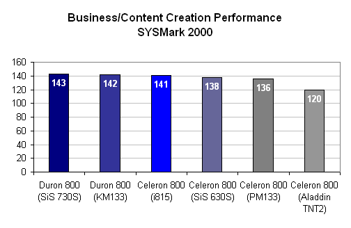
With the systems running at full speed and not limited by the processor not any integrated video solutions, it is clear that Intel's i815 chipset takes the lead when it comes to Socket-370. The performance difference between Intel's 815 chipset and the rest of the Socket370 chipsets out there is bigger than the difference between any other chipsets out there, running around 13% faster than the competition. Next comes the PM133 followed by the SiS 630S.
On the Socket-A side, the performance margin between the chipset solutions out there is rather small. Surprisingly, the KT133 performs slightly faster than the KM133, a chipset that is said to be fundamentally the same as the one in the KT133. The SiS solution, once again, lands at the bottom of the chart.
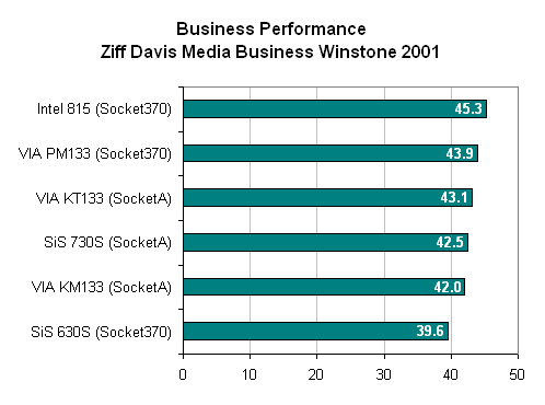
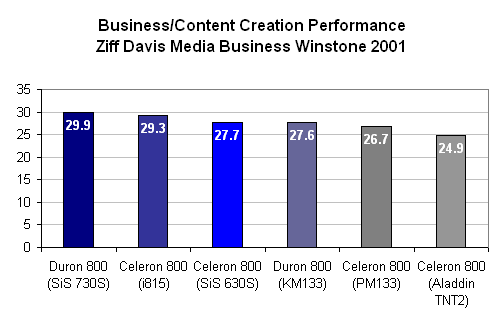
Unlike the SYSmark test, Business Winstone 2001 shows very little difference between chipsets. On the Socket370 side, Intel's 815 chipset slightly edges out over VIA's PM133. The SiS 630S falls short once again, performing the slowest of the three chipsets.
With the Socket-A solutions, VIA's KT133 comes on top, once again edging out the KM133. The SiS 730S actually performs above the KM133 in our Business Winstone tests, leaving the KM133 as the slowest Slot-A chipset this round.
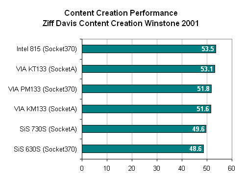
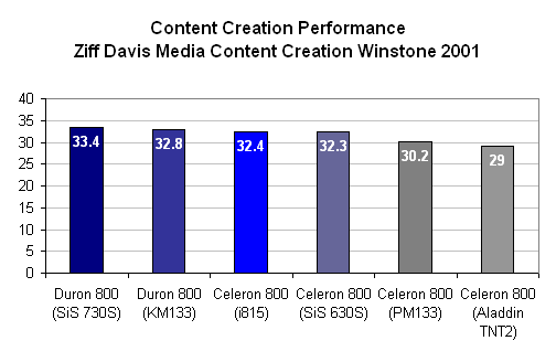
Following previous results, the Intel 815 chipset continues to perform on top of the Socket370 platform. VIA's PM133 solution comes in second place, only performing 3% slower than the 815. The SiS 630S, on the other hand, performed 10% slower than Intel's solution; far from a performance difference that would go unnoticed.
On the Socket-A side, VIA's KT133 chipset continues to score top marks, followed by the KM133 and finally the SiS 730S.
3D Gaming Performance using GeForce2 GTS
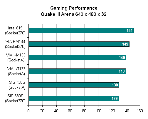
Intel's i815 chipset continues to fall on top of the charts when comparing pure chipset performance. The second fastest Socket370 chipset here is VIA's PM133, performing 4% slower than the 815. The SiS 630S, on the other hand, performed 17% slower than Intel's solution.
With the Socket-A chipsets, we finally see the KM133 and KT133 chipsets performing identically, as VIA said they should. The SiS 730S fell behind both VIA chips by 8%.
With the graph looking very similar to what we have seen before, Intel's i815 chipset proves to be the fastest for the Socket370 platform and VIA's KM133 the fastest for the Socket-A platform.
The trend continues, with the 815 ranking as top dog for the Socket370 and the KT133 top performer for the Socket-A.
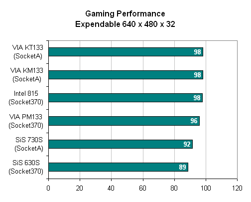
Expendable, a very memory performance-dependent benchmark, shows that there is essentially no difference between the different chipsets with the exception of the poorer performing SiS solutions.
Professional OpenGL Performance using GeForce2 GTS
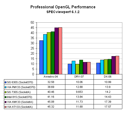
As we have seen in the past, the SiS chipset solutions perform poorly in professional OpenGL tests. Throughout the tests, the KM133 and KT133 Socket-A solutions perform almost identically and happen to perform best of the bunch. The Intel 815 performs fastest of the Socket370 solutions, with the PM133 not falling too far behind.
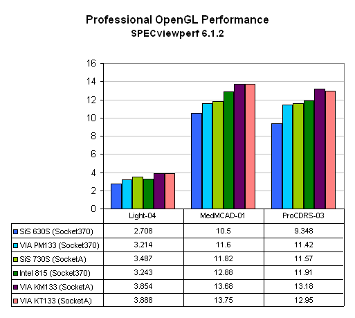
The performance in these three tests reflect the same results found above.
The Real World System Test
Now we switch to showing how the platforms perform on a more realistic value PC setup.
|
Windows 98SE / 2000 Test System |
||||||
|
Hardware |
||||||
|
CPU(s) |
Intel
Celeron 800 MHz
|
AMD Duron 800 MHz |
||||
| Motherboard(s) | ASUS
CUA / Aladin TNT2 Reference Board SiS 630S Reference Board VIA PM133 Reference Board Intel i815 Reference Board |
SiS 730S Reference Board VIA KM133 Reference Board VIA KT133 Reference Board |
||||
| Memory |
128MB PC133 Corsair SDRAM (Micron -7E CAS2) |
|||||
| Hard Drive |
IBM Deskstar 30GB 75GXP 7200 RPM Ultra ATA/100 |
|||||
| CDROM |
Phillips 48X |
|||||
| Video Card(s) |
Integrated
i752 Graphics (i815) |
|||||
| Ethernet |
Linksys LNE100TX 100Mbit PCI Ethernet Adapter |
|||||
|
Software |
||||||
|
Operating System |
Windows
98 SE |
|||||
| Video Drivers |
|
|||||
|
Benchmarking Applications |
||||||
| Gaming |
Unreal
Tournament 4.32 Reverend's Thunder.dem |
|||||
| Productivity |
BAPCo SYSMark 2000 |
|||||
Business/Content Creation Performance using Integrated Video
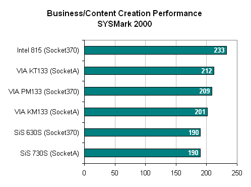
Using the onboard video solutions present in each one of these motherboards, we find that the story has changed quite a bit. No longer is the SiS solution dominated by every other chipset in the field; no, now the SiS 730S chip ranks as the highest Socket-A solution and the SiS 630S is the second fastest Socket370 solution. It seems that SiS can thank their SiS 300 integrated video controller for the sudden speed increase. The KM133 keeps right up with the SiS 730S, however, performing essentially identically to the SiS solution.
The Intel i815 chipset still performs on top of the Socket370 chipsets. The PM133 does not fall far behind, performing in a very similar manner to the i815. Perhaps the most shocking results come with the Aladdin TNT2 chipset, that performs extremely sub par compared to the rest of the solutions.
When relying on the integrated video solutions provided with each chipset, the chipsets all performed nearly identically, with only the KM133 falling slightly behind the rest. The exception to this trend, however, is the poor performance of the Aladdin TNT2 solution.
Again, we see many of the solutions performing virtually identically. All that is about to change...
3D Gaming Performance using Integrated Video
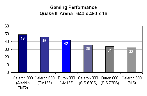
As one may suspect, the Aladdin TNT2 begins to shine when in 3D gaming. Using NVIDIA's graphics core in their integrated solution, ALi is able to beat out all other integrated solutions. In addition, the Aladdin TNT2 is also able to take advantage of its local frame buffer, which can dramatically increase the amount of available memory bandwidth.
The ProSavage core of the PM133 comes next, performing only slightly behind the Aladdin TNT2 solution in Quake III at 640x480x16. We experienced similar results with the ProSavage core of the KM133 as well.
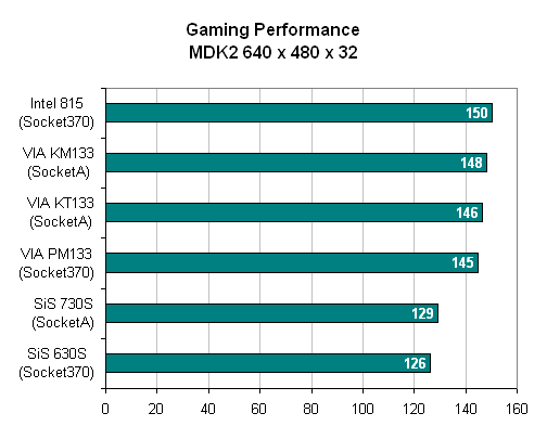
A larger performance drop is realized when going to SiS' 300 integrated graphics core that is found in the SiS 603S and 730S chipsets. And finally, the integrated graphics found on the 815 chipset falls to the bottom of the performance chart, far from its top spot when in 2D graphics.
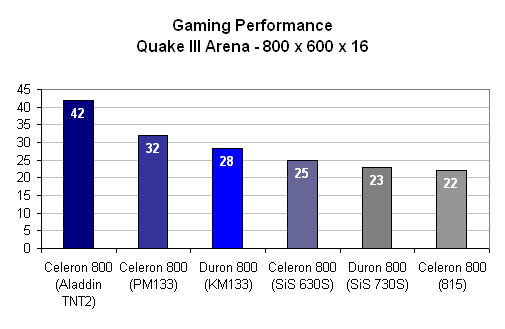
When at 800x600x16, the results are very similar to what we encountered at 640x480x16. It seems that if you are looking for fast gaming performance, the Aladdin TNT2 is the best solution, at least when in Quake III arena, where it is now performing 31% faster than its next fastest competitor.
3D Gaming Performance (cont)
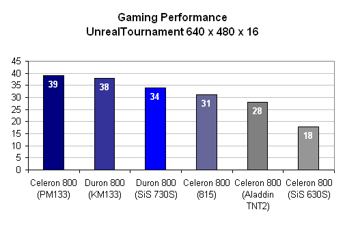
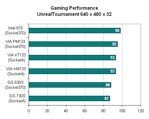
Changing the 3D game to Unreal Tournament switches things up a bit. No longer is the Aladdin TNT2 top 3D performer; it is replaced by the ProSavage core found in both the PM133 and KM133 chipsets. It seems that the ProSavage graphics controller is much better at texture intensive games like Unreal Tournament than it is at high polygon games such as Quake III Arena.
The SiS 300 graphics controller found in the SiS 730S chipset is able to flex enough muscle to keep up with the ProSavage controllers, at least when in the Duron system. The SiS solution for the Socket370 platform does not fare nearly as well, falling way behind the others when it comes to performance. Surprisingly, the i815 chipset is able to out perform two rival chipset solutions, despite the fact that it fell way behind in Quake III Arena tests.
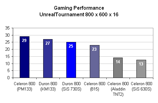
At 800x600x16, we find that the chipsets lie in the same ranking as when in 640x480x16. Once again, the SiS 630S is at the bottom of the graph while the ProSavage based PM133 and KM133 perform best in this situation.
DVD Performance

There is no question that the fact that SiS' integrated solutions include hardware motion compensation and iDCT support help the SiS based chips perform so well in our DVD playback tests. In value systems, it is normally difficult to get good software based DVD playback due to the high amount of processing power this requires. By including both hardware motion compensation and iDCT onto the SiS 300 graphics controller, the SiS 730S and 630S chips essentially dominate the competition.
The Intel i815 solution performed surprisingly well, providing rather low CPU utilization. The Aladdin TNT2 performs next best, with the ProSavage line chips, the KM133 and PM133, resulting in the highest CPU utilization. This is most likely due to the fact that the ProSavage chip seems to be using the Savage4's hardware motion compensation that is most likely not supported in our DVD tests.
Conclusion
Although an integrated video solution may not be the best option for one in seek of a high performance gaming rig, it seems to strike the perfect balance between price and performance for those shopping on a budget. As we have shown, no longer does settling for an integrated chipset solution require abandoning all hopes of 3D gaming. With the technology out there today, it is perfectly possible to play current 3D games in low resolutions with a low color depth. It may not be ideal, but it will work, especially in cases where 3D gaming may come after business related tasks. The problem may not lie in determining that an integrated chipset is the right platform for your next PC, rather it lies in determining which integrated chipset out there is best for your needs.
Choosing the correct integrated video chipset to provide the foundation to your next PC depends mostly on what you plan on doing with the PC. If 2D performance is crucial and 3D game play is an after thought, then Socket370 owners need to look no further than Intel's own i815 chipset. Providing fast 2D performance, the integrated graphics controller found on the i815 will provide plenty of power to get you through any business application and will also have no problem playing your children's non-3D accelerated games. If you are looking for a similar solution on the Socket-A market, the SiS 730S chipset seems to be your cup of tea, providing the fastest 2D performance and great DVD playback ability.
The scene changes dramatically when one is considering an integrated video solution for 3D gaming. Heavy 3D gamers need not apply, as none of the solutions out there now will even come close to the performance level encountered even with a $100 GeForce2 MX. However, if 3D game play is desired, the Aladdin TNT2 chipset seems to be your best bet for upcoming games when using the Socket370 platform. Although performance is sub par in Unreal Tournament, the current trend in games is to produce high polygon scenes like those found in Quake III Arena, meaning that this test should provide a good basis for future game performance. The problem is that the Aladdin TNT2 does not provide support for an external AGP card, meaning that if the game play speed becomes unbearable, the only hope of relief comes in upgrading the whole motherboard. On the Socket-A front, the KM133 seems to be your best bet. Not only does it provide better performance than the competition, it also features an external AGP slot for future upgrades.
With this information in mind, one should now be able to find the best integrated chipset for your next PC. It may be awhile before we see integrated graphics perform at the same speed level as add-in cards in 3D acceleration, but for now they provide a perfect solution for those out there looking for a pure 2D speed at little cost.


