Original Link: https://www.anandtech.com/show/6432/the-intel-ssd-dc-s3700-intels-3rd-generation-controller-analyzed
The Intel SSD DC S3700: Intel's 3rd Generation Controller Analyzed
by Anand Lal Shimpi on November 5, 2012 12:01 PM EST- Posted in
- Storage
- IT Computing
- SSDs
- Intel
- Cloud Computing
Today Intel is announcing its first SSD based on its own custom 6Gbps SATA controller. This new controller completely abandons the architecture of the old X25-M/320/710 SSDs and adopts an all new design with one major goal: delivering consistent IO latency.
All SSDs tend to fluctuate in performance as they alternate between writing to clean blocks and triggering defrag/garbage collection routines with each write. Under sequential workloads the penalty isn't all that significant, however under heavy random IO it can be a real problem. The occasional high latency blip can be annoying on a client machine (OS X doesn't respond particularly well to random high IO latency), but it's typically nothing more than a rare hiccup. Users who operate their drives closer to full capacity will find these hiccups to be more frequent. In a many-drive RAID array however, blips of high latency from each drive can destructively work together to reduce the overall performance of the array. In very large RAID arrays (think dozens of drives) this can be an even bigger problem.
In the past, we've recommended simply increasing the amount of spare area on your drive to combat these issues - a sort of bandaid that would allow the SSD controller to better do its job. With its latest controller, Intel tried to solve the root cause of the problem.
The launch vehicle for Intel's first 6Gbps SATA controller is unsurprisingly a high-end enterprise drive. Since the 2008 introduction of the X25-M, Intel has shifted towards prioritizing the enterprise market. All divisions of Intel have to be profitable and with high margins. The NAND Solutions Group (NSG) is no exception to the rule. With consumer SSDs in a race to the bottom in terms of pricing, Intel's NSG was forced to focus on an area that wouldn't cause mother Intel to pull the plug on its little experiment. The enterprise SSD market is willing to pay a premium for quality, and thus it became Intel's primary focus.
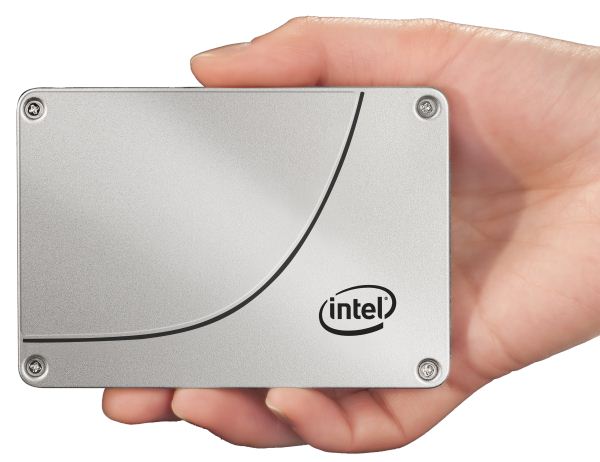
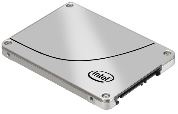
The first drive to use the new controller also carries a new naming system: the Intel SSD DC S3700. The DC stands for data center, which bluntly states the target market for this drive. While it's quite likely that we'll see a version appear in a high-end drive that could be used in a desktop, I don't know that we'll see a mobile version anytime soon for reasons I'll get to later.
The Drive
The S3700 comes in four capacities (100, 200, 400 and 800GB) and two form factors (2.5" and 1.8"). The 1.8" version is only available at 200GB and 400GB capacities. Intel sees market potential for a 1.8" enterprise SSD thanks to the increasing popularity of blade and micro servers. The new controller supports 8 NAND channels, down from 10 in the previous design as Intel had difficulty hitting customer requested capacity points at the highest performance while populating all 10 channels.
The S3700 is a replacement to the Intel SSD 710, and thus uses Intel's 25nm MLC-HET (High Endurance Technology) NAND. The S3700 is rated for full 10 drive writes per day (4KB random writes) for 5 years.
| Intel SSD DC S3700 Endurance (4KB Random Writes, 100% LBA) | ||||||
| 100GB | 200GB | 400GB | 800GB | |||
| Rated Endurance | 10DW x 5 years | 10DW x 5 years | 10DW x 5 years | 10DW x 5 years | ||
| Endurance in PB | 1.825 PB | 3.65 PB | 7.3 PB | 14.6 PB | ||
That's the worst case endurance on the drive, if your workload isn't purely random you can expect even more writes out of the S3700. Compared to the SSD 710, the S3700 sees an increase in endurance even without allocating as much NAND as spare area (~32% vs. 60% on the 710). The increase in endurance even while decreasing spare area comes courtesy of the more mature 25nm MLC-HET process. It's process maturity that's also responsible for Intel not using 20nm NAND on the S3700. We'll eventually see 20nm MLC-HET NAND, but just not now.
Pricing is also much more reasonable than the Intel SSD 710. While the 710 debuted at around $6.30/GB, the Intel SSD DC S3700 is priced at $2.35/GB. It's still more expensive than a consumer drive, but the S3700 launches at the most affordable cost per GB of any Intel enterprise SSD. A non-HET version would likely be well into affordable territory for high-end desktop users.
| Intel SSD DC S3700 Pricing (MSRP) | ||||||
| 100GB | 200GB | 400GB | 800GB | |||
| Price | $235 | $470 | $940 | $1880 | ||
The third generation Intel controller supports 6Gbps SATA and full AES-256 encryption. The controller is paired with up to 1GB of ECC DRAM (more on this later). Intel does error correction on all memories (NAND, SRAM and DRAM) in the S3700.
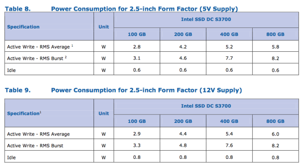
Like previous enterprise drives, the S3700 features on-board capacitors to commit any data in flight on the drive to NAND in the event of a power failure. The S3700 supports operation on either 12V, 5V or both power rails - a first for Intel. Power consumption is rated at up to 6W under active load (peak power consumption can hit 8.2W), which is quite high and will keep the S3700 from being a good fit for a notebook.
Performance & IO Consistency
Performance is much greater than any previous generation Intel enterprise SATA SSD:
| Enterprise SSD Comparison | ||||||
| Intel SSD DC S3700 | Intel SSD 710 | Intel X25-E | Intel SSD 320 | |||
| Capacities | 100 / 200 / 400 / 800GB | 100 / 200 / 300GB | 32 / 64GB | 80 / 120 / 160 / 300 / 600GB | ||
| NAND | 25nm HET MLC | 25nm HET MLC | 50nm SLC | 25nm MLC | ||
| Max Sequential Performance (Reads/Writes) | 500 / 460 MBps | 270 / 210 MBps | 250 / 170 MBps | 270 / 220 MBps | ||
| Max Random Performance (Reads/Writes) | 76K / 36K | 38.5K / 2.7K IOPS | 35K / 3.3K IOPS | 39.5K / 600 IOPS | ||
| Endurance (Max Data Written) | 1.83 - 14.6PB | 500TB - 1.5PB | 1 - 2PB | 5 - 60TB | ||
| Encryption | AES-256 | AES-128 | - | AES-128 | ||
| Power Safe Write Cache | Y | Y | N | Y | ||
Intel is also promising performance consistency with its S3700. At steady state Intel claims the S3700 won't vary its IOPS by more than 10 - 15% for the life of the drive. Most capacities won't see more than a 10% variance in IO latency (or performance) at steady state. Intel has never offered this sort of a guarantee before because its drives would vary quite a bit in terms of IO latency. The chart below shows individual IO latency at steady state (displayed in IOPS to make the graph a bit easier to read) for Intel's SSD 710:
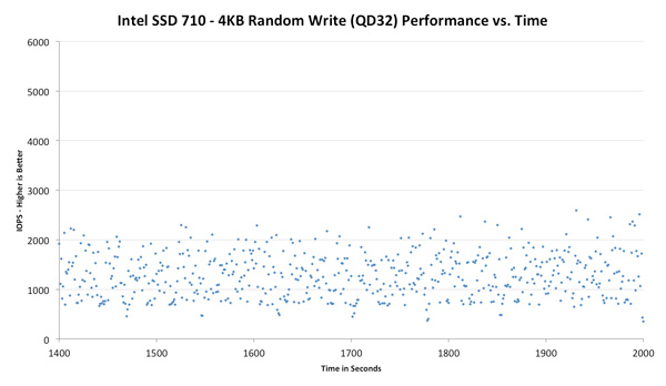
Note the insane distribution of IOs. This isn't just an Intel SSD issue, click the buttons above to look at how Samsung's SSD 840 Pro and the SandForce based 330 do. All of these drives show anywhere from a 2x - 10x gap between worst and best case random write performance over time. Lighter workloads won't look as bad, and having more spare area will help keep performance high, but Intel claims the S3700 is able to tighten its IO latency down to a narrow band of about 10 - 15% variance.
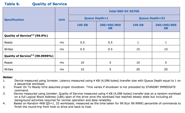
Intel also claims to be able to service 99.9% of all 4KB random IOs (QD1) in less than 500µs:
To understand how the S3700 achieves this controlled IO latency, we need to know a bit more about Intel's older controllers. In researching for this article, I managed to learn more about Intel's first SSD controller than I ever knew before.
A Brand New Architecture
To understand how the S3700 is different, we need to revisit how SSDs work. I've done this several times over the years so I'll keep it as succinct as possible here. SSDs are made up of a bunch of NAND packages, each with 1 - 8 NAND die per package, with each die made of multiple planes, blocks and finally pages.
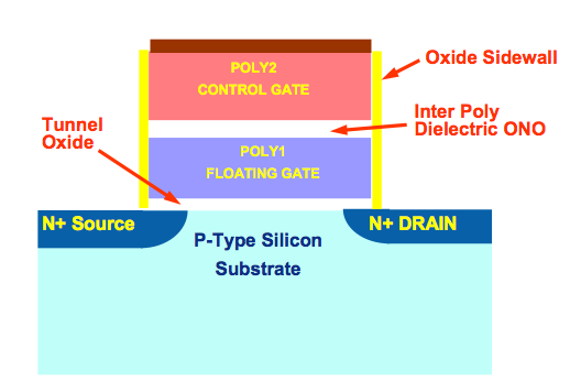
NAND is solid-state, non-volatile memory (data is retained even when power is removed, courtesy of some awesome physics). There are no moving parts, and accesses are very memory-like which delivers great sequential and random IO performance. The downside is NAND has some very strict guidelines dictating how it is written to and erased.
The first thing to know about NAND flash is that you can only write to the same NAND cell a finite number of times. The total amount of charge stored in a NAND cell is counted in dozens of electrons. The tunneling process that places the electrons on the floating gate (thus storing data) weakens the silicon oxide insulation layer that keeps the charge there. Over time, that layer degrades to the point where the cell can no longer store data, and it has to be marked as bad/unusable.
The second principle of dealing with NAND is that you can only write to NAND at the page level. In modern drives that's a granularity of 8KB.
The final piece of the puzzle, and the component that makes all of this a pain to deal with is that you can only erase NAND at the block level, which for Intel's 25nm NAND is 256 pages (2048KB).
Modern SSDs present themselves just like hard drives do, as a linear array of logical block addresses. The OS sends an address and command to the SSD, and the controller translates that address to a physical location in NAND.
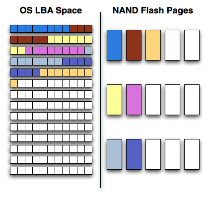
When writing to an SSD, the SSD controller must balance its desire for performance (striping writes across as many parallel NAND die as possible) with the goal of preserving NAND lifespan by writing to all cells evenly (wear leveling).
As writes come in, new pages are allocated from a pool of free blocks. As the process of erasing a NAND cell reduces endurance, a good SSD controller will prefer allocating an empty page for new data over erasing an old block. Eventually the controller will run out of clean/empty pages to write to and will have to recycle an old block filled (sometimes only partially) with invalid data to keep operating. This process can reduce overall performance and increase wear on the NAND.
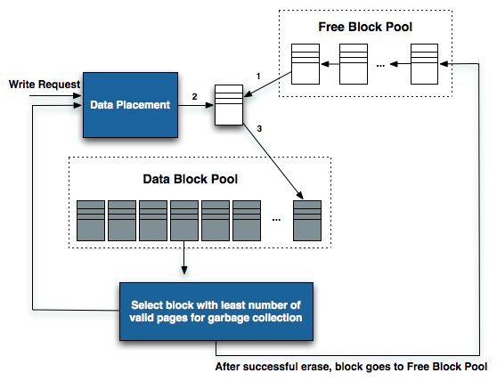
When writing sequential data to an SSD it's easy to optimize for performance. Transfers can be broken up and striped across all available NAND die. Reading the data back is perfectly optimized for high performance as well. It's random IO that causes a problem for performance. Writes to random LBA locations are combined and sent out as burst traffic to look sequential, however the mapping of those LBAs to physical NAND locations can leave the drive in a very fragmented state. With enough random data fragmented on a drive, all write performance will suffer as the controller will no longer be able to quickly allocate large contiguous blocks of free pages across all NAND die.
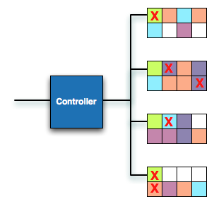
SSD in a fragmented state, white blocks represent free pages, Xes represent invalid data, colored blocks are valid data - more detail here
Modern SSD controllers will attempt to defragment themselves either while the drive is in use, or during periods of idle time (hence the phrase idle garbage collection). Adequate defragmentation is necessary to maintain a drive's performance even after it has been used for a while. The best controllers do a great job of defragmenting themselves as they work, while the worst allow internal fragmentation to get out of hand.
With that recap out of the way, let's talk about how Intel's first and second generation SSD controllers worked.
The Indirection Table
There never was a true Intel X25-M G3, the third generation controller went missing after briefly appearing on Intel roadmaps. Instead we got mild revisions of the X25-M G2's controller with new features enabled through firmware. This old controller was used in the Intel SSD 320 and more recently in the Intel SSD 710.
One notable characteristic of this old controller was that it never required a large external DRAM (16 - 64MB for the early drives). Intel was proud of the fact that it stored no user data in DRAM, which I always assumed kept the size requirements down. It turns out there was another reason.
All controllers have to map logical block addresses to physical locations in NAND. This map is stored on the NAND itself (and wear leveled so it actually moves locations), but it's cached in DRAM for fast access. Intel calls this map its indirection table.
In the old drives, the indirection table was a binary tree. A binary tree is a data structure made up of nodes and branches where each node can have at most two children.
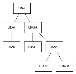
An example of an LBA-tracking binary tree, Intel's implementation is obviously far more complex. This tree can get huge.
The old indirection table grew in size as the drive was written to. Each node would keep track of a handful of data including logical block address and the physical NAND location that the block mapped to. The mapping wasn't 1:1 so many nodes would refer to a starting LBA address in addition to an offset, allowing a single node to refer to a range of physical locations.
As write requests came in, sequential data was stored as LBA + offset per node in the binary tree. Non-sequential data created a new node, growing the tree, and increasing lookup time. The tree remained balanced (for low-overhead searches, comp sci majors will remember that there's a direct relationship between the height of a binary tree and how long it takes to perform inserts/lookups on the tree), so the creation of new nodes could sometimes be very time intensive.
Given the very small DRAM that Intel wanted on its drives (to help keep costs as low as possible) and the increasing lookup times from managing an ever expanding tree, Intel would regularly defragment/compress the tree. With enough data in the tree you could actually begin compressing various nodes in the tree down into a single node. For example we might have two separate nodes in the tree that refer to sequential physical locations, which can be combined into a single node with location + offset. The tree defrag/compression process would contribute to high latency with random IO.
There was another problem however. The physical NAND had to be defragmented on a regular basis to keep pages contiguous and avoid a random sprinkling of pages on each block (this can negatively impact sequential IO performance if you go to write a large block of data and it either has to be split up amongst multiple randomly distributed blocks, or if you have to erase and rewrite a bunch of blocks to make room for the new data). The problem was that once NAND was defragmented, the logical to physical mapping tree had to be updated to reflect the new mapping, which could sometimes conflict. There could be situations where the tree could just be finished compressing itself, but the NAND would defrag itself forcing a recompression/reorganization of the tree. The fact that both the mapping tree and physical NAND had to be defragmented, and the fact that doing one could create more work for the other contributed to some potentially high latencies in the old design.
The old Intel controller had to defragment both the indirection table and the physical NAND space, and the two processes could conflict, which would create some unexpectedly high latency IO from time to time. On average, Intel was able to keep this under control, but when given the opportunity to start from scratch one major goal was to eliminate this cause of latency.
The New Indirection Table
While the binary tree structure was great for sequential IO performance and for keeping DRAM sizes low, it wasn't good for lowering random IO latency. The S3700 controller completely does away with the old indirection table.
The new controller ditches the binary tree entirely and moves to a completely flat structure with 1:1 mapping. What happens now is there's a giant array with each location in the array mapped to a specific portion of NAND. The array isn't dynamically created and, since it's a 1:1 mapping, searches, inserts and updates are all very fast.
The other benefit of being 1:1 mapped with physical NAND is that there's no need to defragment the table, which immediately cuts down the amount of work the controller has to do. Drives based on this new controller only have to keep the NAND defragmented.
The downside to all of this is the DRAM area required by the new flat indirection table. The old binary tree was very space efficient, while the new array is just huge. It requires a large amount of DRAM depending on the capacity of the drive. In its largest implementation (800GB), Intel needs a full 1GB of DRAM to store the indirection table. By my calculations, the table itself should require roughly 100MB of DRAM per 100GB of storage space on the drive itself. Intel appears to be using DDR3-1333 for its DRAM on-board S3700 drives.
There's a bit of space left over after you account for the new indirection table. That area is reserved for a cache of the controller's firmware so it doesn't have to read from slow flash to access it.
Once again, there's no user data stored in the external DRAM. The indirection table itself is physically stored in NAND (just cached in DRAM), and there are two large capacitors on-board to push any updates to non-volatile storage in the event of power loss.
It sounds like a simple change, but building this new architecture took quite a bit of work. The results, if they are anywhere close to what Intel is promising, are pretty awesome.
Final Words
The Intel SSD DC S3700 appears to be a very promising new architecture from Intel. If it ends up performing as Intel promised, the S3700 controller could be the beginning of a new era in SSD performance - one focused on consistency of performance, not just absolute performance. As soon as we run samples through our test suite you can expect a full review, putting Intel's claims to the test. Stay tuned.

