Original Link: https://www.anandtech.com/show/4830/intels-ivy-bridge-architecture-exposed
Intel's Ivy Bridge Architecture Exposed
by Anand Lal Shimpi on September 17, 2011 2:00 AM EST- Posted in
- CPUs
- Intel
- Ivy Bridge
- IDF 2011
- Trade Shows
Five years ago Intel announced its ambitious tick-tock release cadence. We were doubtful that Intel could pull off such an aggressive schedule but with the exception of missing a few months here or there tick-tock has been a success. On years marked by a tick Intel introduces a new manufacturing process, while tock years keep manufacturing process the same and introduce a new microprocessor architecture. To date we've had three tocks (Conroe, Nehalem, Sandy Bridge) and two ticks (Penryn, Westmere). Sampling by the end of this year and shipping in the first half of next year will be Intel's third tick: Ivy Bridge.
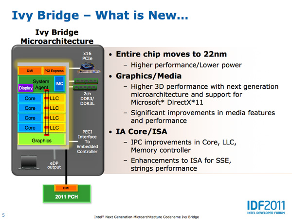
Ivy Bridge (IVB) is the first chip to use Intel's 22nm tri-gate transistors, which will help scale frequency and reduce power consumption. As we already mentioned, mobile Ivy Bridge will be the first Intel CPU to bring four cores into a 35W TDP.
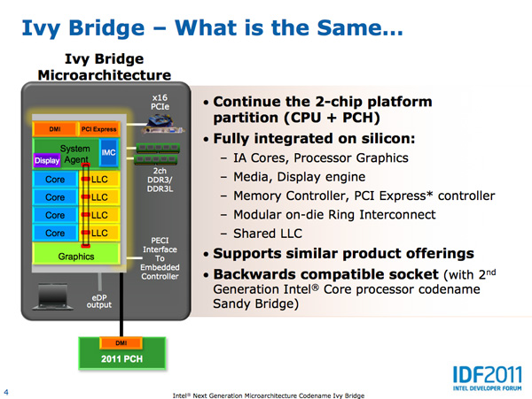
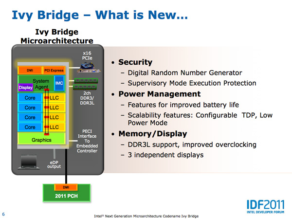
At a high level Ivy Bridge looks a lot like Sandy Bridge. It's still a monolithic die that features an integrated GPU. The entire die is built at 22nm, continuing Intel's march towards truly addressing integrated graphics performance. Ivy Bridge won't get rid of the need for a discrete GPU but, like Sandy Bridge, it is a step in the right direction.
Intel hasn't announced die size but transistor count has increased to approximately 1.4 billion (layout). This is up from 1.16 billion in Sandy Bridge, a 20.7% increase. With perfect scaling a 22nm Sandy Bridge die would be 47.3% the size of a 32nm die. Even with the increase in transistor count, it's a good bet that Ivy Bridge will be noticeably smaller than Sandy Bridge.
Motherboard & Chipset Support
Ivy Bridge is backwards compatible with existing LGA-1155 motherboards, although there will be a new chipset for Ivy Bridge and new motherboards to enable some features (e.g. PCI Express 3.0, native USB 3.0). The new chipset family falls under the 7-series banner. We'll see Z77, Z75, H77, Q77, Q75 and B75 available at or around launch.
| Chipset Comparison | ||||||||
| Z77 | Z75 | H77 | Z68 | P67 | H67 | |||
| CPU Support |
IVB LGA-1155 |
IVB LGA-1155 |
IVB LGA-1155 |
SNB/IVB LGA-1155 |
SNB/IVB LGA-1155 |
SNB/IVB LGA-1155 |
||
| CPU Overclocking | Yes | Yes | No | Yes | Yes | No | ||
| CPU PCIe Config |
1 x16 or 2 x8 or 1 x8 + 2 x4 PCIe 3.0 |
1 x16 or 2 x8 PCIe 3.0 |
1 x16 PCIe 3.0 |
1 x16 or 2 x8 or 1 x8 + 2 x4 PCIe 3.0 |
1 x16 or 2 x8 PCIe 3.0 |
1 x16 PCIe 3.0 | ||
| Processor Graphics Support | Yes | Yes | Yes | Yes | No | Yes | ||
| Intel SRT (SSD caching) | Yes | No | Yes | Yes | No | No | ||
| RAID Support | Yes | Yes | Yes | Yes | Yes | Yes | ||
| USB 2.0 Ports (3.0) | 14 (4) | 14 (4) | 14 (4) | 14 | 14 | 14 | ||
| SATA Total (Max Number of 6Gbps Ports) | 6 (2) | 6 (2) | 6 (2) | 6 (2) | 6 (2) | 6 (2) | ||
| PCIe Lanes | 8 (5GT/s) | 8 (5GT/s) | 8 (5GT/s) | 8 (5GT/s) | 8 (5GT/s) | 8 (5GT/s) | ||
As I mentioned above, Ivy Bridge finally supports USB 3.0 natively. The consumer 7-series chipsets feature 14 total USB ports, 4 of which are USB 3.0 capable. The CPU itself features 16 PCIe (1x16, 2x8 or 1x8 + 2x4) gen 3 lanes to be used for graphics and/or high performance IO. You will only see Gen 3 speeds on qualified motherboards. It's technically possible on 6-series motherboards but guaranteed on 7-series motherboards. The Z77 and H77 chipsets will support Intel's Smart Response Technology (SRT, aka SSD caching) which is a Z68 exclusive today.
SATA and chipset-attached PCIe slots haven't changed. Overclocking is supported on all Z-chipsets, while the H-chipset doesn't. All chipsets support Intel's HD Graphics, which is a departure from the Sandy Bridge mess where P67 didn't.
Core Architecture Changes
Ivy Bridge is considered a tick from the CPU perspective but a tock from the GPU perspective. On the CPU core side that means you can expect clock-for-clock performance improvements in the 4 - 6% range. Despite the limited improvement in core-level performance there's a lot of cleanup that went into the design. In order to maintain a strict design schedule it's not uncommon for a number of features not to make it into a design, only to be added later in the subsequent product. Ticks are great for this.


Five years ago Intel introduced Conroe which defined the high level architecture for every generation since. Sandy Bridge was the first significant overhaul since Conroe and even it didn't look very different from the original Core 2. Ivy Bridge continues the trend.
The front end in Ivy Bridge is still 4-wide with support for fusion of both x86 instructions and decoded uOps. The uOp cache introduced in Sandy Bridge remains in Ivy with no major changes.
Some structures within the chip are now better optimized for single threaded execution. Hyper Threading requires a bunch of partitioning of internal structures (e.g. buffers/queues) to allow instructions from multiple threads to use those structures simultaneously. In Sandy Bridge, many of those structures are statically partitioned. If you have a buffer that can hold 20 entries, each thread gets up to 10 entries in the buffer. In the event of a single threaded workload, half of the buffer goes unused. Ivy Bridge reworks a number of these data structures to dynamically allocate resources to threads. Now if there's only a single thread active, these structures will dedicate all resources to servicing that thread. One such example is the DSB queue that serves the uOp cache mentioned above. There's a lookup mechanism for putting uOps into the cache. Those requests are placed into the DSB queue, which used to be split evenly between threads. In Ivy Bridge the DSB queue is allocated dynamically to one or both threads.
In Sandy Bridge Intel did a ground up redesign of its branch predictor. Once again it doesn't make sense to redo it for Ivy Bridge so branch prediction remains the same. In the past prefetchers have stopped at page boundaries since they are physically based. Ivy Bridge lifts this restriction.
The number of execution units hasn't changed in Ivy Bridge, but there are some changes here. The FP/integer divider sees another performance gain this round. Ivy Bridge's divider has twice the throughput of the unit in Sandy Bridge. The advantage here shows up mostly in FP workloads as they tend to be more computationally heavy.
MOV operations can now take place in the register renaming stage instead of making it occupy an execution port. The x86 MOV instruction simply copies the contents of a register into another register. In Ivy Bridge MOVs are executed by simply pointing one register at the location of the destination register. This is enabled by the physical register file first introduced in Sandy Bridge, in addition to a whole lot of clever logic within IVB. Although MOVs still occupy decode bandwidth, the instruction doesn't take up an execution port allowing other instructions to execute in place of it.
ISA Changes
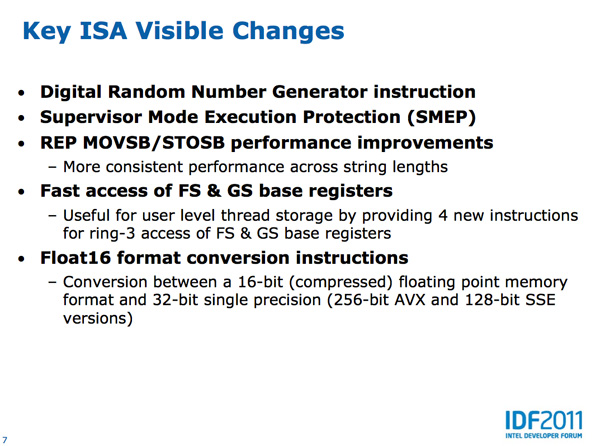
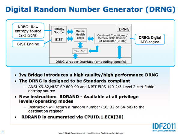
Intel also introduced a number of ISA changes in Ivy Bridge. The ones that stand out the most to me are the inclusion of a very high speed digital random number generator (DRNG) and supervisory mode execution protection (SMEP).
Ivy Bridge's DRNG can generate high quality random numbers (standards compliant) at 2 - 3Gbps. The DRNG is available to both user and OS level code. This will be very important for security and algorithms going forward.
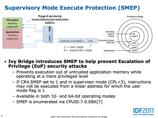
SMEP in Ivy Bridge provides hardware protection against user mode code being executed in more privileged levels.
Cache, Memory Controller & Overclocking Changes
Despite the title of this section, to my knowledge there haven't been any changes to Ivy Bridge's cache. The last level cache (L3) is still shared via a ring bus between all cores, the GPU and the system agent. Quad-core Ivy Bridge CPUs will support up to 8MB of L3 cache, and the private L1/L2s haven't increased from their sizes in Sandy Bridge (32+32K/256K).
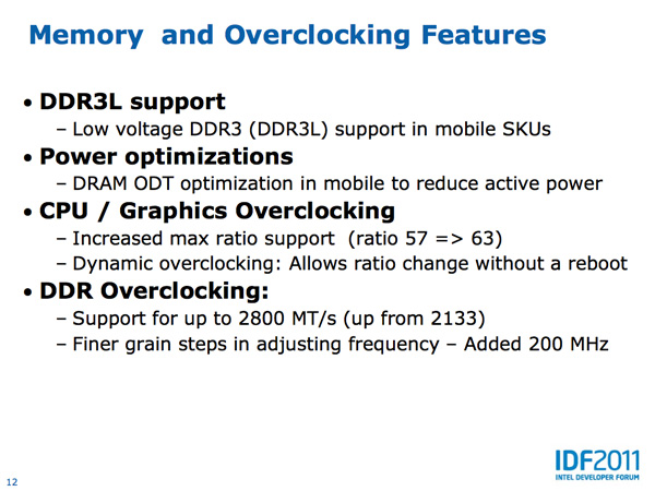
The memory controller also remains relatively unchanged, aside from some additional flexibility. Mobile IVB supports DDR3L in addition to DDR3, enabling 1.35V memory instead of the standard 1.5V DDR3. This is particularly useful in notebooks that have on-board DDR3 on the underside of the notebook; OEMs can use DDR3L and keep your lap a bit cooler.
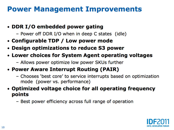
From Nehalem to Sandy Bridge, Intel introduced fairly healthy amounts of power gating throughout the processor. With little more to address in Ivy Bridge, Intel power gated one of the last available portions of the die: the DDR3 interface. If there's no external memory activity, the DDR3 interface can now be turned off completely. External IOs leak current like any other transistor so this change makes sense. Power gating simply increases die size but at 22nm Intel should have some extra area to spend on things like this.
Memory overclocking also gets a bump in Ivy Bridge. The max supported DDR3 frequency in SNB was 2133MHz, Ivy Bridge moves this up to 2800MHz. You can now also increase memory frequency in 200MHz increments.
Power Efficiency Improvements
When Intel introduced its 22nm tri-gate transistors Intel claimed that it could see an 18% increase in performance at 1V compared to its 32nm process. At the same switching speed however, Intel's 22nm transistors can run at 75 - 80% of the voltage of their 32nm counterparts. Ivy Bridge's process alone should account for some pretty significant power savings. In addition to process however, there are a few architectural changes in IVB that will reduce power consumption.

Lower System Agent Voltages
Sandy Bridge introduced the System Agent, a name that used to refer to the uncore of a processor but now refers to the display output, memory controller, DMI and PCI Express interfaces. As of Sandy Bridge, the L3 cache was no longer included in the uncore and thus it wasn't a part of the System Agent.
The System Agent operates on a separate voltage plane than the rest of the chip. On Ivy Bridge Intel now offers even lower System Agent voltage options for the lower voltage SKUs, which in turn helps power optimize those SKUs.
More Accurate Voltage Characterization
Today Intel defines three different voltages for every Sandy Bridge CPU: LFM, nominal and turbo. LFM is the lowest frequency the CPU can run at (e.g. completely idle), nominal is the frequency it is specified to run at (e.g. 3.3GHz for a 2500K) and turbo is the highest available turbo frequency (e.g. 3.7GHz for a 2500K). Intel determines the lowest voltage possible for each one of those frequencies. Sandy Bridge obviously runs at more than just three frequencies, there are many more intermediate frequencies that it may run at depending on the current workload. The voltages at those intermediate frequencies are interpolated from the three points that I mentioned above.
With Ivy Bridge, Intel characterizes even more points along the frequency curve. Intel didn't reveal exactly how many points but it's more than three. A curve is then fit to the frequency/voltage data and depending on IVB's operating frequency a more accurate voltage point is calculated. The result from all of this seemingly simple work is a reduction in core voltage at these intermediate frequencies. Voltage changes have a cubic affect on power, so even a small reduction here can have a tangible impact. One of the points that wasn't previously characterized was max thread turbo. Ivy Bridge should be more power efficient in cases where you have all cores active.
Power Aware Interrupt Routing
This next feature is pretty neat. Ivy Bridge has logic to properly route interrupt requests to cores that are already awake vs. those that are asleep in their lowest power states. Obviously this approach can save a lot of power, however it may rob those active cores of some performance. IVB will allow prioritizing performance as well. Interrupt handling can thus be handled similarly to how it is today, or optimally for power savings.
Configurable TDP
I already wrote about what this is but if you missed our Pipeline post on it I'll briefly recap. All CPUs ship with a rated thermal design point (TDP) that tells OEMs what sort of cooling the chip requires. Traditionally that TDP value remained static and the CPU could do whatever it wanted but exceed that value. Ivy Bridge introduces configurable TDP that allows the platform to increase the CPU's TDP if given additional cooling, or decrease the TDP to fit into a smaller form factor.
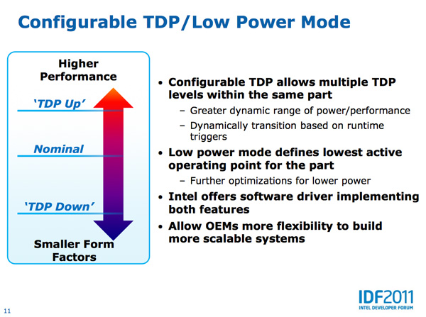
The cTDP up mode is obviously for docked notebooks. You can imagine an Ivy Bridge notebook with an optional dock that could enhance the cooling capabilities of the machine. When undocked the notebook's processor would operate at a max TDP of 17W, for example, but toss it in a dock with additional cooling and the TDP would jump up to 33W. It's up to the OEMs to decide how they want to take advantage of this feature. It could be something as simple as a mobile dock with more fans, or something as complex as a modular water cooling solution with a bigger radiator in the dock. I haven't seen any concepts of systems that take advantage of Ivy Bridge's cTDP up support, but that's the theory.
What about cTDP down? Take the same 17W Ivy Bridge CPU from above but now drop the TDP to 13W, which in turn limits clock speed and voltage. Why would you want to do this? From the OEM perspective, Intel's TDP choices may seem arbitrary. Downwards configurable TDP allows OEMs to get a lower power configuration without forcing Intel to create a new SKU. OEMs can do this today through undervolting/underclocking of their own, but the cTDP down spec will at least give OEMs a guarantee of performance/power.
Configurable TDP obviously only applies to mobile Ivy Bridge. In particular the ultra low voltage and extreme edition parts will support cTDP. The cTDP values are listed in the table below:
| Ivy Bridge Configurable TDP | |||||
| cTDP Down | Nominal | cTDP Up | |||
| Ivy Bridge ULV | 13W | 17W | 33W | ||
| Ivy Bridge XE | 45W | 55W | 65W | ||
The most interesting are the 17W ULV Ivy Bridge parts as far as I'm concerned. Today you do sacrifice clock speed to get into the form factor of a MacBook Air. A clever OEM armed with Ivy Bridge might be able to deliver a cooling dock that would give you the best of both worlds: an ultra portable chassis on the go, and higher clock speeds while docked.
The New GPU
Westmere marked a change in the way Intel approached integrated graphics. The GPU was moved onto the CPU package and used an n-1 manufacturing process (45nm when the CPU was 32nm). Performance improved but it still wasn't exactly what we'd call acceptable.
Sandy Bridge brought a completely redesigned GPU core onto the processor die itself. As a co-resident of the CPU, the GPU was treated as somewhat of an equal - both processors were built on the same 32nm process.
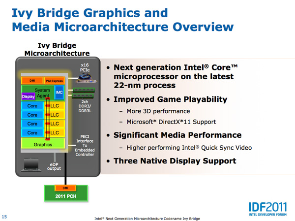
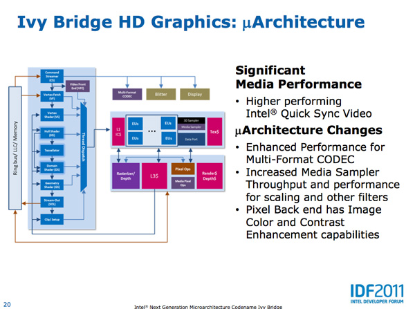
With Ivy Bridge the GPU remains on die but it grows more than the CPU does this generation. Intel isn't disclosing the die split but there are more execution units this round (16 up from 12 in SNB) so it would appear as if the GPU occupies a greater percentage of the die than it did last generation. It's not near a 50/50 split yet, but it's continued indication that Intel is taking GPU performance seriously.
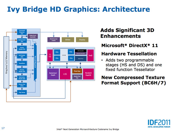
The Ivy Bridge GPU adds support for OpenCL 1.1, DirectX 11 and OpenGL 3.1. This will finally bring Intel's GPU feature set on par with AMD's. Ivy also adds three display outputs (up from two in Sandy Bridge). Finally, Ivy Bridge improves anisotropic filtering quality. As Intel Fellow Tom Piazza put it, "we now draw circles instead of flower petals" referring to image output from the famous AF tester.
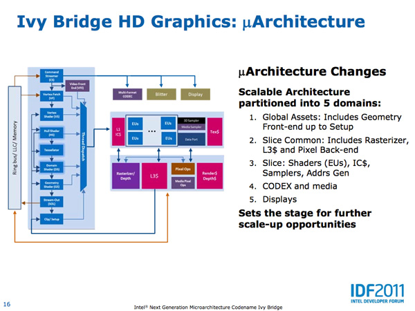
Intel made the Ivy Bridge GPU more modular than before. In SNB there were two GPU configurations: GT1 and GT2. Sandy Bridge's GT1 had 6 EUs (shaders/cores/execution units) while GT2 had 12 EUs, both configurations had one texture sampler. Ivy Bridge was designed to scale up and down more easily. GT2 has 16 EUs and 2 texture samplers, while GT1 has an unknown number of EUs (I'd assume 8) and 1 texture sampler.
I mentioned that Ivy Bridge was designed to scale up, unfortunately that upwards scaling won't be happening in IVB - GT2 will be the fastest configuration available. The implication is that Intel had plans for IVB with a beefier GPU but it didn't make the cut. Perhaps we will see that change in Haswell.
As we've already mentioned, Intel is increasing the number of EUs in Ivy Bridge however these EUs are much better performers than their predecessors. Sandy Bridge's EUs could co-issue MADs and transcendental operations, Ivy Bridge can do twice as many MADs per clock. As a result, a single Ivy Bridge EU gets close to twice the IPC of a Sandy Bridge EU - in other words, you're looking at nearly 2x the GFLOPS in shader bound operations as Sandy Bridge per EU. Combine that with more EUs in Ivy Bridge and this is where the bulk of the up-to-60% increase in GPU performance comes from.
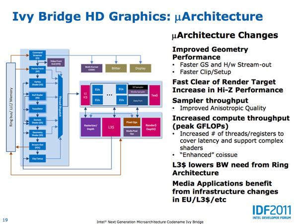
Intel also added a graphics-specific L3 cache within Ivy Bridge. Despite being able to share the CPU's L3 cache, a smaller cache located within the graphics core allows frequently accessed data to be accessed without firing up the ring bus.
There are other performance enhancements within the shader core. Scatter & gather operations now execute 32x faster than Sandy Bridge, which has implications for both GPU compute and general 3D gaming performance.
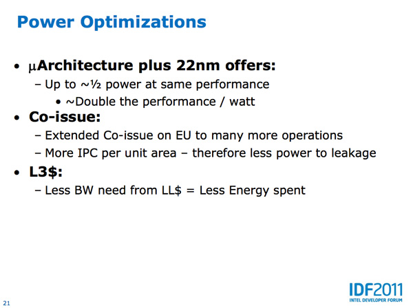
Despite the focus on performance, Intel actually reduced the GPU clock in Ivy Bridge. It now runs at up to 95% of the SNB GPU clock, at a lower voltage, while offering much higher performance. Thanks primarily to Intel's 22nm process (the aforementioned architectural improvements help as well), GPU performance per watt nearly doubles over Sandy Bridge. In our Llano review we found that AMD delivered much longer battery life in games (nearly 2x SNB) - Ivy Bridge should be able to help address this.


Quick Sync Performance Improved
With Sandy Bridge Intel introduced an extremely high performing hardware video transcode engine called Quick Sync. The solution ended up delivering the best combination of image quality and performance of any available hardware accelerated transcoding options from AMD, Intel and NVIDIA. Quick Sync leverages a combination of fixed function hardware, IVB's video decode engine and the EU array.
The increase in EUs and improvements to their throughput both contribute to increases in Quick Sync transcoding performance. Presumably Intel has also done some work on the decode side as well, which is actually one of the reasons Sandy Bridge was so fast at transcoding video. The combination of all of this results in up to 2x the video transcoding performance of Sandy Bridge. There's also the option of seeing less of a performance increase but delivering better image quality.
I've complained in the past about the lack of free transcoding applications (e.g. Handbrake, x264) that support Quick Sync. I suspect things will be better upon Ivy Bridge's arrival.
Final Words
Ivy Bridge will bring about higher clock speeds thanks to its 22nm process, however the gains will likely be minimal at best. Intel hasn't been too keen on pursuing clock speed for quite some time now. Clock for clock performance will go up by a small amount over Sandy Bridge (4 - 6%), combine that with slightly higher clock speeds and we may see CPU performance gains of around 10% at the same price point with Ivy Bridge. The bigger news will be around power consumption and graphics performance.
Ivy Bridge will be Intel's flagship 22nm CPU for some time. The chip was originally due out at the end of this year but was likely subject to delays due to issues with the fab process and the chip itself. The move to 22nm is significant leap. Not only are these new transistors aggressively small but the introduction of Intel's tri-gate technology is a major departure from previous designs. Should the fab engineers at Intel do their job well, Ivy Bridge could deliver much better power characteristics than Sandy Bridge. As we've already seen, introducing a 35W quad-core part could enable Apple (and other OEMs) to ship a quad-core IVB in a 13-inch system.
Ivy Bridge's GPU performance is particularly intriguing. With a 33% increase in execution hardware and a near doubling of performance per EU, it's clear that Intel is finally taking GPU performance seriously. If Intel can hit its clock and performance targets, Ivy Bridge could deliver GPU performance on-par with AMD's Llano. By the time Ivy Bridge arrives however, AMD will have already taken another step forward with Trinity. The question is who will address their performance issues quicker? Will AMD improve x86 performance faster than Intel can improve GPU performance? Does it even matter if both companies end up at the same point down the road? Short of 3D gaming workloads, I believe that x86 CPU performance is what sells CPUs today. Intel's embracing of OpenCL however and AMD's efforts in that space imply things are finally changing in that regard.
Sandy Bridge brought about a significant increase in CPU performance, but Ivy seems almost entirely dedicated to addressing Intel's aspirations in graphics. With two architectures in a row focused on improving GPU performance, I do wonder if we might see this trend continue with Haswell. Intel implied that upward scalability was a key goal of the Ivy Bridge GPU design, perhaps we will see that happen in 2013.
Ivy Bridge can do very well in notebooks. A more efficient chip built using lower power transistors should positively impact battery life and thermal output. Desktop users who already upgraded to Sandy Bridge may not feel the pressure to upgrade, but having better graphics shipping on all new systems can only be good for the industry.


