Original Link: https://www.anandtech.com/show/2850
Budget Micro-ATX P55 Faceoff: Gigabyte GA-P55M-UD2 and ASRock P55M Pro
by Gary Key on October 5, 2009 12:30 PM EST- Posted in
- Motherboards
Mini-ITX is the new Micro-ATX, and Micro-ATX is the new ATX. At least that’s where we see the trends going in the next few years. With the heavy amount of integration that Intel is working on, motherboard real estate just isn’t as important as it used to be.
While we won’t be able to buy an LGA-1156 mini-ITX motherboard until early 2010, there are good micro-ATX options for Lynnfield owners today with more coming.
The price points are nice and you don’t give up any features to go with a micro-ATX P55 motherboard. Gigabyte’s GA-P55M-UD2 is selling for $110 and ASRock’s P55M Pro lists for $99. We will take a look at the performance oriented Gigabyte GA-P55M-UD4 and ASUS Maximus III GENE motherboards shortly. While both those boards are targeted to gamers/overclockers with dual x16 PCIe slots (x8 dual in CF/SLI) along with additional features, better performance is not necessarily a given unless you are running multi-GPU or high-end cooling options.
You also don’t give up much in the way of features with either of these boards. Both offer a single PCIe x16 slot for graphics support along with an x4 PCIe 2.0 slot. ASRock gives you a single PCIe x1 and a 32-bit PCI slot, while Gigabyte insists on a pair of 32-bit PCI slots. Both boards also feature IEEE 1394a, eSATA, Gigabit LAN, 8-channel audio, and a penchant for overclocking. The Gigabyte UD2 board ups the stakes with two additional 3Gbps SATA ports and a BIOS that just about any enthusiast will love in an entry-level board.
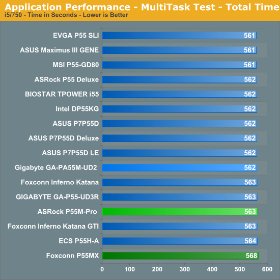
Performance is indistinguishable from other P55 motherboards - these things all perform about the same at stock speeds:
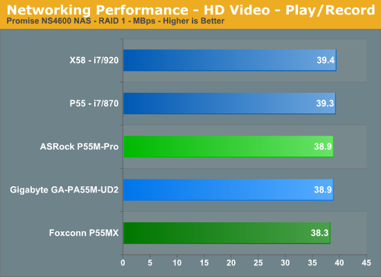
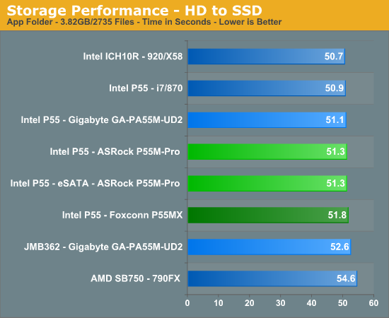
Networking and storage performance are about equal between the two boards as well:
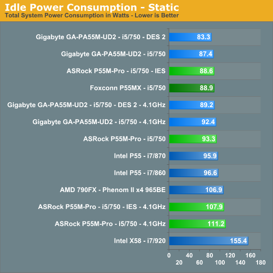
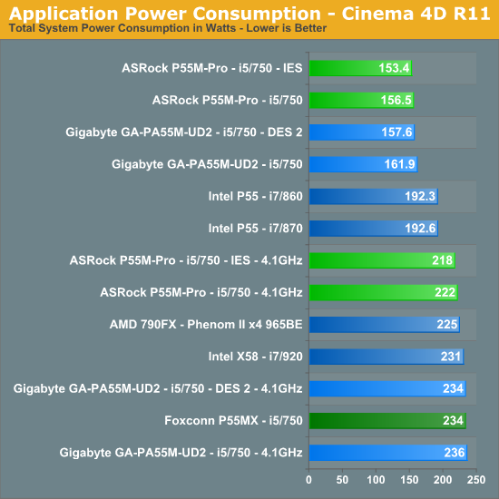
The biggest difference between the boards, from a stock performance standpoint, actually surfaces in power consumption:
About the only real performance difference between these two motherboards is in overclocking.
Core i7/860 8GB Results -
Gigabyte GA-P55M-UD2
ASRock P55M Pro
If you’re going to buy just one, we’d recommend the Gigabyte GA-P55M-UD2, especially if top flight overclocking is important to you. If you are not concerned solely with overclocking, then the ASRock P55M Pro is a great choice, especially if you are on a strict budget and it comes with our full recommendation. If you want more details on both boards, continue on.
P55 Chipset Overview
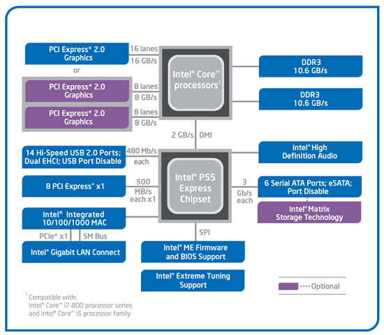
We have just one chipset now as typical Northbridge functions are moved onto the Lynnfield processor. Just like its Bloomfield-based Core i7 big brother, Lynnfield based CPUs have integrated memory controllers. The DDR3 memory channels are dual channel unlike the triple channel setup on Bloomfield. Lynnfield currently supports 16GB of memory, solidly placing it in the midrange category. However, official memory speeds now reach 1333MHz instead of 1066MHz on Bloomfield. The biggest difference between the two processer families is that Lynnfield stuffs 16 lanes of PCI Express 2.0 connectivity into the processor, thus alleviating the need for a Northbridge.
Those 16 PCIe 2.0 lanes can be configured as a single x16 link or split between a pair of x8s for multi-GPU configurations with a set of PCIe switches. CrossFireX support is a given but SLI support depends upon the motherboard manufacturer providing the right amount of funds to Nvidia for certification. For those unwilling to just accept 16 PCIe 2.0 lanes, EVGA already has a P55 board featuring the nForce 200 bridge chip with full support for three-way SLI.
What was known as the Integrated Controller Hub (ICH) on previous chipsets (such as the ICH10R) is now referred to as the P55 Express Platform Controller Hub, or PCH. The chip is based on 65-nm process technology. As such, it is a lot smaller than the ICH10 series with a total die area of around 76.5 mm².
| AMD SB750 | Intel ICH10R | Intel P55 | |
| Additional PCI Express | None | 6 x1 PCIe 1.1 | 8 x 1 PCIe 2.0 |
| USB | 12 ports | 12 ports | 14 ports |
| SATA (300MB/s) | 6 ports | 6 ports | 6 ports |
| PATA | 2 channels | None | None |
| RAID* | RAID 0/1/5/10 | RAID 0/1/5/10 | RAID 0/1/5/10 |
| HD Audio Interface | Yes | Yes | Yes |
| Ethernet | Not Integrated | Intel Gigabit LAN | Intel Gigabit LAN |
| Northbridge Interface | 4 lane PCIe 1.1 | DMI 1Gb/s each direction, full duplex | DMI 1Gb/s each direction, full duplex |
The P55 Express PCH provides six 3 Gb/s SATA ports, 14 USB 2.0 ports, a Gigabit Ethernet MAC , HD Audio interface, and eight lanes of PCI Express 2.0 goodness all for about $40. That price tag buys you two additional USB ports and two additional PCIe lanes over the $3 ICH10R. One other change worth mentioning is that the Gigbit Ethernet MAC will use one of those PCIe lanes if enabled.
The PCI Express lanes are version 2.0 but Intel decided to limit their speed to PCIe 1.x specs at 2.5GT/s. Why? We believe with the DMI link continuing to operate at 1GB/s in each direction, a decent 6Gb/s SAS/SATA RAID card and a few upcoming 6Gb/s drives could easily saturate the link. The P55 Express PCH consumes a little over 4.5W during normal operation. Considering the specifications on AMD’s upcoming SB8xxx chipsets, it appears we have a PCH Gap brewing.
First up is Gigabyte’s GA-P55M-UD2. You can purchase this board for around $105~$110.
Gigabyte GA-P55M-UD2 Feature Set
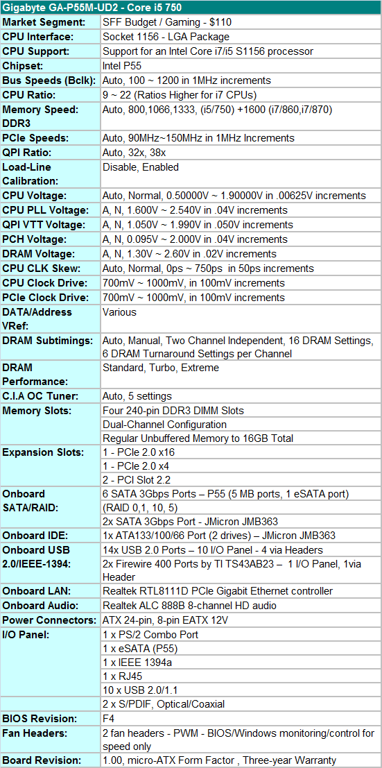
Gigabyte includes the standard array of components like the Realtek ALC888B HD audio codec, Realtek RTL8111D Gigabit LAN controller, T.I. TSB43AB23 IEEE 1394a chipset, GSATA2 (JMB363) chipset, and full support for the Core i7/i5 S1156 processor series.
Gigabyte also includes a rather sparse accessories bundle. You get the standard rear I/O panel cover along with 1 x IDE cable, 2 x SATA cables, a well-written and informative manual, and software CD. We understand the need to cut costs where possible to meet a $100 price target, but including at least one USB 2.0 and IEEE 1394a bracket for the headers would have been appreciated.
BIOS
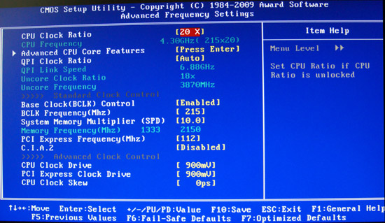
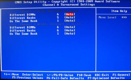
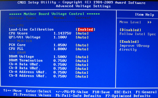
Gigabyte also includes one of the most extensive BIOS designs in an entry level micro-ATX motherboard that we have seen recently. The BIOS is setup for overclocking and includes all the basic settings: CPU multiplier, PCI-E bus, Bclk frequency, memory multipliers, and nearly every voltage setting you will need. Gigabyte includes Load Load-Line Calibration (LLC) and PCH Core (P55) voltage settings for additional overclocking duties. LLC will help to eliminate line droop on the VCore line. We still recommend having LLC disabled in most situations, but if you have to reach a certain overclock for benchmarking, then you should probably enable it. Generally, we do not need PCH voltages in our experience but it is nice to have the feature.
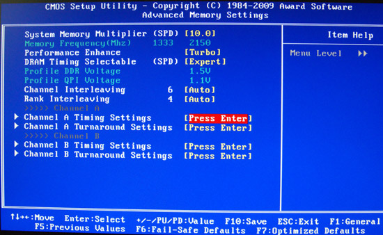
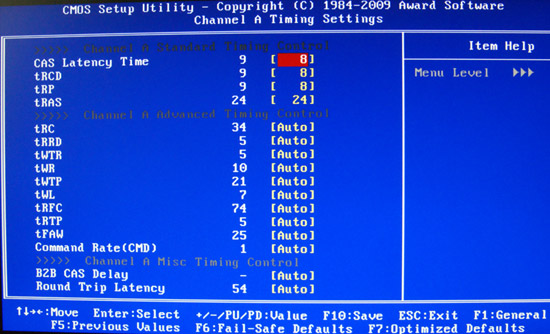
Two strengths of the BIOS are the granular voltage settings and memory timing options for an entry level board. Gigabyte allows you to tweak CPU clock skews, channel independent DRAM settings, and CPU/PCI clock drives although we found the auto settings to be just about perfect.
One last feature we would like to mention is the Q-Flash utility that is accessed via the F8 key. Q-Flash can read files directly from a USB flash drive making BIOS updating a simple and safe procedure. We tried this feature 30 times as part of our testing routine and it never failed.
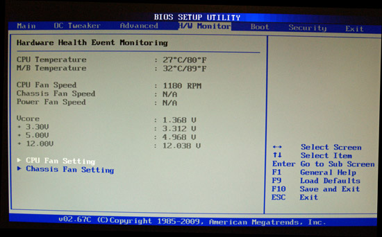
We did have a couple of slight disappointments with the BIOS. In the voltage setting options, Gigabyte does not provide the base voltages that the board defaults to at startup. Our other complaint has to do with the PC Health section, as the lack of SmartFan adjustments for the lone chassis header is not available. The CPU SmartFan adjustment for the CPU is limited to Auto/Voltage/PWM without the ability to determine temperature ranges. Oh how do we miss abit’s uGuru technology. Other than that, we were impressed with the BIOS considering the entry level nature of the board.
BIOS Information
Let’s take a brief look at the BIOS. We discussed the features earlier, but a visual representation sometimes speaks louder than words.
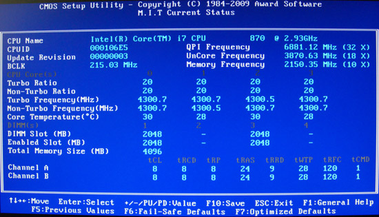


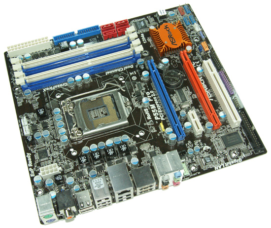
Gigabyte GA-P55M-UD2 Layout
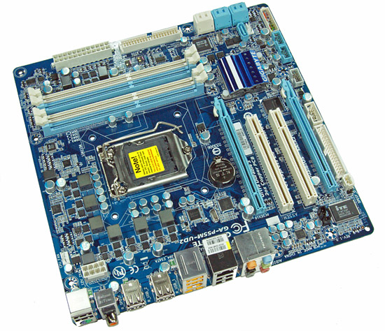
Considering the limited board space, Gigabyte did a very good job fitting all of the peripherals onto this board. About the only negatives we can think of is the continued inclusion of the floppy drive port, lack of passive cooling for the MOSFET area, and only two fan headers. The board does support CrossFireX operation although we highly recommend against this setup as the second PCIe x16 slot is actually an x4 electrical slot running off the P55 chipset with performance suffering up to 30% depending on the choice of video card and game.
The UD2 features Gigabyte's UltraDurable 3 technology that features their 2oz. copper based PCB, solid capacitors, low RDS(on) MOSFETs, and ferrite core chokes.
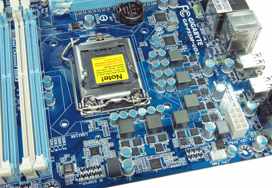
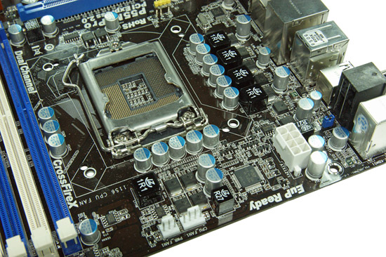
Gigabyte utilizes a high quality four-phase plus one PWM setup on this board. The CPU area is open for the most part and will accommodate larger coolers like the Thermalright Ultra 120 eXtreme. Large push/pull coolers like the Vigor Monsoon III LT will block the first DIMM slot and potentially can interfere with the first PCIe x16 slot.
We originally thought additional airflow across the MOSFETs would be required to ensure 24/7 stability when overclocking. However, the MOSFETs only reached 58.6C under full load with our i7/860 operating at 4.2GHz. We ran the board for 200 hours in with this overclock setting with the case fans turned off. This left just the Corsair 750HX providing air exhaust capabilities.
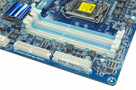
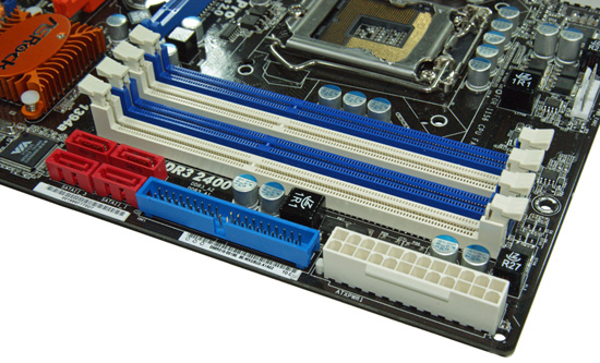
The IDE port, 24-pin ATX power connector, and the four DIMM slots are located in the lower right hand corner of the board. This board supports dual channel memory configurations and 16GB of DDR3 memory when using 4GB DIMMS. Installing the memory with a video card inserted in the first slot is difficult but not impossible.
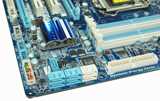
There are five (blue) SATA 3Gb/s ports provided by the P55 chipset that support RAID 0, 1, 5, 10. The sixth port available on the P55 (under the blue heatsink) is utilized on the I/O panel for eSATA. Gigabyte includes the JMicron JMB363 3Gb/s SATA chip that drives the two white SATA ports and provides IDE support. The front panel header, two USB headers, and the IEEE 1394a header are located at the edge of the board.
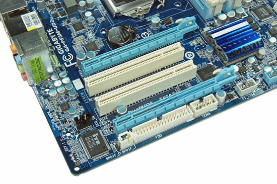
Gigabyte includes two PCIe x16 slots (x16 operation for the first slot, x4 operation for the second slot) and two PCI slots. The first PCI slot will be unavailable when utilizing a dual slot video card.
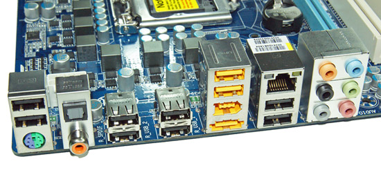
Last but not least is the I/O panel. We have ten USB 2.0 ports (total of fourteen on the board), combination PS/2 port, single eSATA port from the P55, IEEE 1394a port offered by the TI TSB43AB23 chipset, Gigabit Ethernet LAN port via the Realtek RTL8111D chipset, optical out/coaxial out S/PDIF ports, and the audio panel that provides 8-channel audio output via the Realtek ALC 888B HD audio codec.


Tech
One of the highlighted features that Gigabyte implemented in the GA-P55M-UD2 motherboard is the Ultra Durable 3 technology. Ultra Durable 3 features lower ESR solid capacitors, lower RDS(on) MOSFETs, and ferrite core chokes. Gigabyte now rates the longevity of the solid capacitors at 50,000 hours or approximately 6 years of continuous use.
The second major improvement cited by Gigabyte in their Ultra Durable 3 design is the introduction of a 2-ounce copper PCB for both the Power and Ground layers compared to the typical 1-ounce layers found in most consumer boards. Gigabyte claims this technology offers substantially lower system temperatures, superior energy efficiency, and improved overclocking. We can verify the temperature and energy efficiency claims; at least compared to other boards in this price sector at idle conditions.
DPC Latency
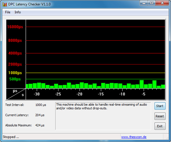
We get a lot of requests for DPC latency results on each board we test. The latency variations between manufacturers utilizing the same chipset vary more than one might imagine. In the past, Gigabyte has had problems in this area when others did not. We are happy to report that it appears those problems are thing of the past. All of our P55 boards so far have exhibited the same behavior in this benchmark. Our test used the Core i5/750 at stock settings with 8GB of memory installed with timings set to 6-6-6-18 at DDR3-1333.
Software
GIGABYTE provides several software applications with the GA-P55M-UD2, EasyTune6, D.E.S 2, and Smart 6 being the three main ones.
EasyTune6
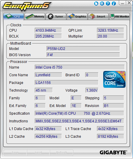
GIGABYTE's EasyTune6 application provides monitoring, system information, and overclocking capabilities. This is one of the better applications provided by the various motherboard suppliers for tuning a system within Windows. We would still like to see additional voltage readings and the ability to save the settings to the BIOS - or at least a BIOS profile. The version shipped on the driver CD did not allow Bclk changes, but the updated version on the website works correctly.
We still prefer tuning within the BIOS. Other than that, this application is useful for extracting a decent amount of performance improvement out of the system after booting Windows. One benefit of such an approach is that you can reduce performance - along with power requirements and the stress on a system - without rebooting.
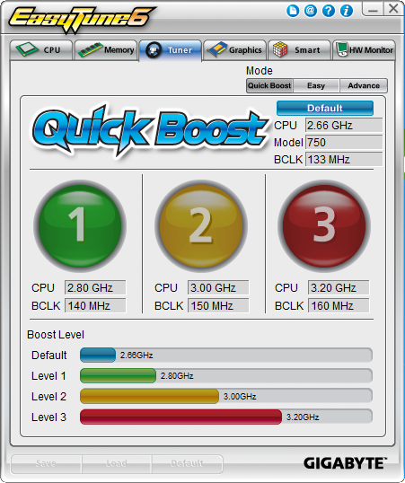
Quick Boost mode is a simple way for novice users to quickly overclock their systems without entering the BIOS. Once you click on one of the three boost levels, the utility will automatically optimize system settings according to your specific hardware combination. A reboot is required since this not an on-the-fly routine. The program is based on algorithms of hardware that has been pre-tested by GIGABYTE engineers unlike the MSI and ASUS offerings that evaluate your actual hardware configuration.
We tried around fifteen different hardware combinations and all worked correctly. Of course, it should work as the single core turbo mode on the i5/750 hits 3.2GHz without a problem, even when undervolting. Of course, with the Level 3 overclock, all four cores will be operating at 3.2GHz which comes in handy with video/audio encoding or 3D rendering programs. Although our memory kit was capable of C7 settings at DDR3-1600, at least this application set the board to DDR3-1600 speeds. Otherwise, the aggressive turbo modes on the Lynnfield processors have just about made this particular feature useless.
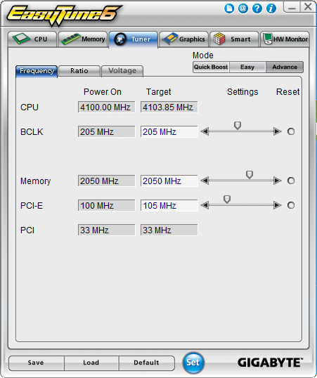
For those who appreciate and want a manual approach to overclocking, the Tuner tab has two different options. Easy mode allows control over Bclk, but it is Advance mode that opens several on-the-fly tweaking options that actually work. You can adjust Bclk, memory speed, PCI-E frequency, and numerous voltage options.
We have to say that using EasyTune6 was an almost painless experience although we prefer BIOS tuning on this platform. During the more extreme overclocking tests, this was the first application we loaded after getting the OS installation up and running. ET6 can be a huge help in tweaking those final settings to find a motherboard's overclocking limits.
DES 2
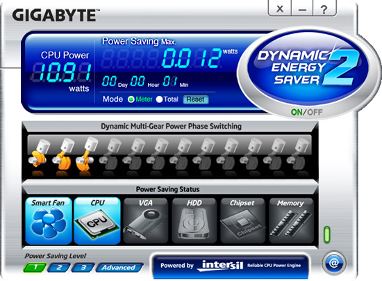
One of the most highly touted features from GIGABYTE is their Dynamic Energy Saver (DES 2) advanced power management solution. GIGABYTE provides a Windows-based software application to control DES 2. After installing the software (we highly recommend downloading the latest version) and a quick reboot, the application is ready for use. The control panel is powered down by default and it is up to the user to turn it on with a simple click of the DES button.
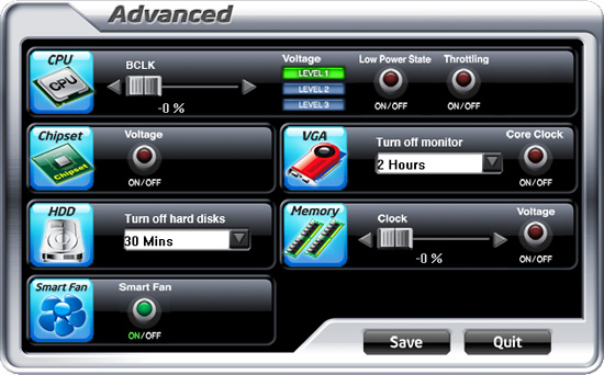
The DES software is simple to use and easy to understand. GIGABYTE provides a power savings meter in the top portion providing us with power savings information that can be reset at startup; otherwise it will track the power savings since the installation of the product. Real-time CPU power usage is available along with a graphic representation of the phases in use. You can also enable CPU throttling to save additional power during operation. The advanced tab lets you set power saving options for other peripherals, although we did not notice any additional power savings compared to Windows 7 default setup.
GIGABYTE also includes an onboard LED system that indicates the number of phases in use. These LEDs can be turned on and off from the control panel. The user can utilize DES while the system is overclocked although we typically did not measure any power savings in CPU bound applications, but games tended to respond well with a 3%~9% power savings.
Smart 6

Gigabyte also includes their new Smart6 software package that consists of Smart Quickboot, Smart Quickboost, Smart Recovery, Smart DualBIOS, Smart Recorder, and Smart Timelock. Smart Quickboot is a simple way to quickly set S3 sleep state in the BIOS and enable Hibernation in Windows. Smart Quickboost is the auto overclock application in ET6.
Smart Recovery is a method to quickly backup files or directories but not complete OS images. The unusual feature here is that even reformatting the drive will retain this hidden partition and data. We tried, it works. Smart DualBIOS is a personal recorder for saving important dates or password in the BIOS. Even if you lose this information in the OS, it is still retained. The downside is that reflashing the BIOS wipes the data clean. SmartRecorder is basically a time logging program to track access times and monitor file changes. Smart Timelock is a software application that can lockout a PC user for a certain period of time, but the time period considers a day to be only eight hours.


Overclocking
GIGABYTE advertises the GA-P55M-UD2 as an entry level P55 motherboard and will nudge users towards their enthusiast-oriented UD4P or UD5 series for overclocking duties. We are here to say that on most air-cooling or even water-cooling setups, it makes no difference whether you are using this board or one of the $220+ P55 boards. They all tend to reach the same 210~220 Bclk range with memory hitting 2133 or a little higher. The primary differences between the “entry-level” boards and the more expensive enthusiast level boards will be in memory overclocking, BIOS features, and possibly stability at the higher Bclk rates.
Now, memory overclocking really only matters for setting benchmark records, the additional BIOS features is something most everyone can live without, and stability in reaching a 222MHz Bclk compared to 215MHz Bclk (on air) will only matter to those who like to post CPU-Z screenshots or run SuperPi/3DMarks as their primary applications. For those on advanced cooling, the more expensive boards are designed to handle those requirements, but you are not going to run your system 24/7 with these cooling methods and probably want an i7/X58 platform for that purpose anyway.
So for those of us on a budget but still wanting a very good overclocking experience, the Gigabyte P55M-UD2 will cover just about every need one can ask for in a P55 motherboard. We expected solid overclocking based on the BIOS design and board components, but this board clocked just as well or better than any upper-end P55 boards we have in the labs.
True, there are boards that will hit higher Bclk rates or offer better memory performance, but we are concentrating on practical overclocking capabilities in our tests. We focus on the type of overclocks that support 24/7 operation with reasonable cooling and the ability to run a multitude of programs without a problem. We are not optimizing for SuperPi, 3DMark records, or to get that one extra Bclk for a CPUZ screenshot. We put an emphasis on stability during our testing sessions so we test with real world applications ranging from a variety of games to digital imaging software to various audio/video creation programs, and 3D rendering programs in multitask situations.
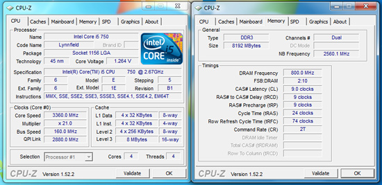
We have tested a variety of retail Core i5/750 processors over the past several weeks. Our particular sample (L926B) used in testing will hit 4.1GHz with decent air cooling on 1.375V VCore on average. Some boards require less voltage and some require more, but we consider 1.375V to be the median average. The latest retail processors (L928B) are running at 4.2GHz on the same voltage but we have already completed testing with the earlier stepping. Of course, getting a really good retail CPU is a roll of the dice for the most part.
As much as most motherboard suppliers would like you to believe that the board design and cost is going to have the greatest impact on overclocking, that is really not true with the Lynnfield/P55 platform with air or water cooling. The most significant impact on overclocking this platform will be directly attributable to the quality of the CPU and your cooling choice, provided your motherboard has overclocking options.
We tend to keep to our voltages around 1.375V with the Lynnfield processors and air cooling as heavy load multitask temperatures will reach around 80C with very good air cooling. Typical gaming situations and single task application usage will see temperatures hit the 57C~65C range under full load conditions over a period of an hour or so. We could add more voltage, but with our current 750, it would only get us to 4.2GHz and any performance differences are not noticeable without a benchmark.
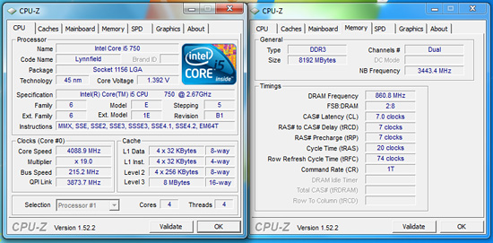
Core i5/750 8GB Results
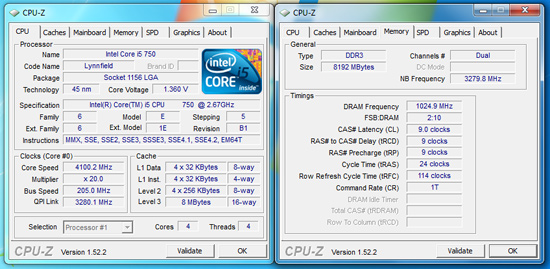
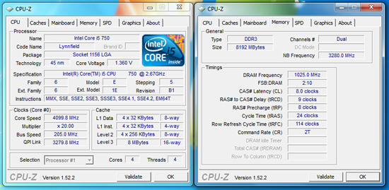
Our maximum stable overclock on air-cooling with the Core i5/750 resulted in a 4.1GHz clock speed at a respectable 205MHz Bclk with a variety of 8GB DDR3-2000+ memory kits from G.Skill , Patriot, OCZ, Kingston, and Corsair. The primary voltages settings were 1.375V VCore, 1.37V VTT, 1.80V PLL, and 1.66V VDimm.
In the end, we settled on 20x205. Our Patriot and Kingston memory kits would run either at 8-9-8-24 2T or 9-9-9-24 1T on 1.66V, increasing voltage did not allow us to run 1T at CAS8 with these lower binned Elpida Hyper kits. However, performance was identical between the two settings. Vdroop was approximately -.005V with Load Line Calibration (LLC) enabled and -.01V with it disabled at idle. Under load Vdroop was -.015V with LLC enabled and -.03V with it disabled.
We could increase Bclk to 215 and drop our CPU multiplier to 19, but that required a VTT increase to 1.41V, memory to 1.70V (due to the increased memory speed) , and PLL to 1.86V. Performance was not any different from our 20x205 setting in application testing. In fact, dropping our memory multiplier to 8x for a DDR3-1720 setting resulted in timings at 7-7-7-20 1T at 1.64V and VTT dropping to a decent 1.350V range. Application performance was generally the same between the two memory settings and at times favored the DDR3-1720 C7 setup.
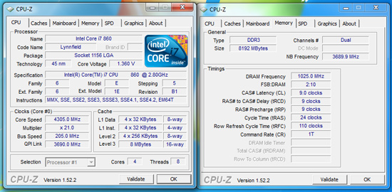
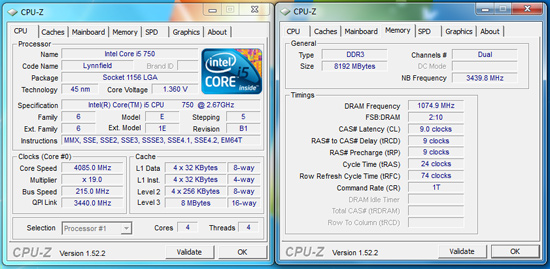
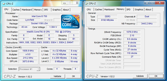
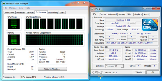
Core i7/860 8GB Results
Our i7/860 fared better clocking wise than the i5/750. We ended up at a perfectly stable 21x205 setting resulting in a 4.3GHz clock speed with 8GB at DDR3-2050 at 9-9-9-24 1T timings. However, our voltage settings changed a little with VTT at 1.39V, PLL at 1.86V, VDimm at 1.66V, and VCore at 1.375V. Under load Vdroop was -.015V with LLC enabled and -.03V with it disabled.
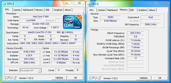
Core i7/870 8GB and 4GB DDR3-2400 Results
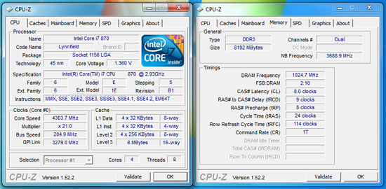
We know most people will not purchase the Core i7/870 and if they do, it is probably not going into a $110 motherboard. Our intent in showing this screenshot is that we simply left all of the voltage settings on auto except for VDimm. It took about ten seconds in the BIOS to get this overclock. The board settings were extremely close to our manual settings with the exception being VTT and VDimm.
VTT was set to 1.41V which is acceptable for this overclock level and memory settings, manually this clock speed needed 1.39V VTT. The problem was with VDimm, as soon as the memory clocks exceeded 2000, the board would auto set to 1.80V. That voltage is something our Elpida Hyper IC kits do not like. We ended up changing VDimm to 1.66V.
Gigabyte advertised DDR3-2400 speeds so we decided to verify their claim. Sure enough, the board had no problem running our OCZ DDR3-2400 Blade kit at 2400 with the stock 9-10-9-24 1T settings on 1.66V.


Thoughts
We have absolutely no concerns about recommending this board for 24/7 overclocking use. This board overclocks Core i7 processors just as easily as it does the Core i5 offerings, which is a feat several of the upcoming budget/mid-range P55 boards cannot accomplish. To be honest here, overclocking a Lynnfield processor is extremely easy; really, you only need to worry about VCore, VDimm, VTT, and occasionally PLL settings. If you get a really good CPU, such as our current i7/860 sample, it makes overclocking really easy, even if you just woke up from a coma and your last memory was playing pong at a disco club. What made our overclocking experience enjoyable was the fact that this board is so easy to operate with up to its limits. It simply is a great motherboard to own for quick and stable overclocks.
In regards to voltage regulation, we think the GA-P55M-UD2 has very
good voltage output. We checked all the major voltages with a DMM and found
very little variance between what you select in the BIOS and what the board
actually outputs. The VTT, PLL, DIMM, and other voltages are accurate and
stable across the spectrum until you hit the upper limits of current draw. As a side bonus, S3 resume worked perfectly with Bclks up to 215.
This is not a board to have for extreme clocking as I would not run CPU voltages higher than 1.45V on it without expecting something to fail, rather quickly I might add. It is perfectly suited for air-cooling and typical water cooling setups and one should not expect more. I was initially concerned about the lack of passive MOSFET cooling. With our voltage settings and stated goal of practical overclocking for the majority of users, it is not a problem, even with the Core i7/860 at 4.3GHz under full load. We typically measured MOSFET temps around 61C at 4.3GHz and around 58C at 4.2GHz without any direct airflow over the board. I would still recommend a well ventilated case for these types of overclocks.
Next up is ASRock’s P55M Pro. You can purchase this board for around $100.
ASRock P55M Pro Feature Set
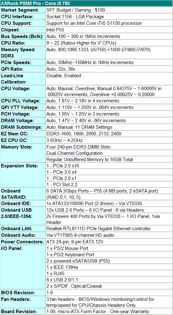
ASRock includes a full featured set of components like the Via VT1708S HD audio codec, Realtek RTL8111D Gigabit LAN controller, Via VT6330 IDE/IEEE 1394a combo chipset, powered eSATA/USB ports on the I/O panel, and full support for the Core i7/i5 S1156 processor series.
ASRock also includes a limited accessories bundle. You get the standard rear I/O panel cover along with 1 x IDE cable, 1 x Floppy cable, 2 x SATA cables, 1 x SATA power cables, an informative manual and quick installation guide, and software CD. We understand the need to cut costs where possible to meet a $100 price target, but including at least one USB 2.0/IEEE 1394a bracket for the headers would have been appreciated.
BIOS
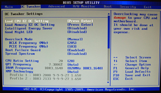
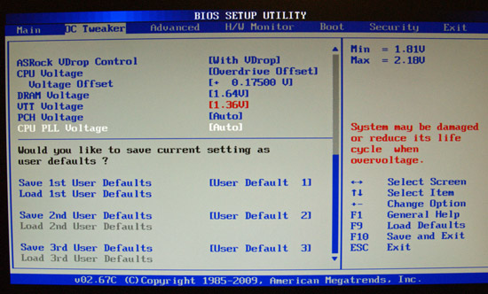
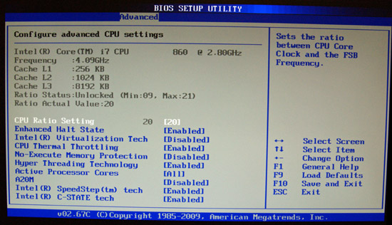
ASRock has designed a BIOS that emphasizes quick auto overclock settings using their CPU or Memory presets rather manually overclocking the board. The breadth of granular BIOS settings in the Gigabyte UD2 board is just not available in the P55M Pro . The BIOS is setup for general overclocking duties and includes the typical P55 settings: CPU multiplier, PCI-E bus, Bclk frequency, memory multipliers, and important voltage options needed for overclocking.
ASRock includes Load Load-Line Calibration (LLC), or they refer to it as With or Without Vdrop. LLC will help to eliminate line droop on the VCore line, but also will cause VCore to overshoot set values when under load. We recommend having LLC disabled in most situations, but if you have to reach a certain overclock for benchmarking, then you should probably enable it. In our case, we enabled when overclocking above 3.8GHz since Vdrop was around -0.05V under load in most cases.
One strength of the BIOS is the auto OC settings that will quickly set the board up for overclocking your memory or CPU to a preset level. Both settings worked well with us favoring the CPU settings as the memory setting at 2133/2400 would drop the CPU multiplier to 13x~15x, resulting in CPU speeds lower than stock with Turbo disabled.
Our only problem with the CPU OC setup is that memory speeds would sometime drop below the capability of our kits with memory speeds running in the 1200MHz range. Those speeds actually do not penalize application performance by more than a couple of percent, but timings followed the SPD of the module. If the SPD is not setup properly, you could end up with CAS 9/10 settings at DDR3-1200. It is easy enough to change them but you end up defeating the purpose of a quick OC.
Voltages tended to range on the high side with the CPU auto OC settings. We understand the reasoning as the ranges needed to ensure stability across a wide variety of processor capabilities require running VCore/VTT a little higher than our CPU’s capabilities. This is the one drawback to preset settings utilized by Gigabyte and ASRock instead of auto overclocking routines based on actual component capabilities that ASUS utilizes. The good news is that on the CPU side, our system always reached the presets and was perfectly stable. Using the memory presets above DDR3-2000 resulted in a few lockups, especially with memory that had not been tested by ASRock.
ASRock has finally implemented BIOS flashing within the BIOS. Instant Flash can read files directly from a USB flash or hard drive making BIOS updating a simple and safe procedure. We tried this feature 30 times as part of our testing routine and it never failed.
We did have a couple of slight disappointments with the BIOS. In the voltage setting options, ASRock does not provide granular voltage settings in the same way that Gigabyte does on the UD2 board. The settings provided will allow for quick and easy overclocks to the 4.1GHz range. Practically speaking, that is probably a level we would not exceed in a 24/7 desktop to be honest.
However, it was a limiting factor in overclocking this board compared to the Gigabyte offering. The main culprit was the lack of VTT voltages between 1.36V and 1.42V. We feel that exceeding 1.40VTT could create a long term problem with Lynnfield CPUs. Intel’s guidance is still 1.35V as the recommended maximum, if not lower in most cases with these CPUs. We needed around 1.39V on VTT to ensure stable operation with our processors above 4.1GHz, we just would not run the 1.42V setting in the ASRock BIOS on air-cooling for performance improvements that would be minor on a daily basis.
BIOS Information
Let’s take a brief visual look at the BIOS.
ASRock P55M Pro Layout
ASRock designed a very good layout for this board. The same negatives apply for this board as it did for the Gigabyte UD2, that is the continued inclusion of the floppy drive port, lack of passive cooling for the MOSFET area, and only two of the three fan headers offer temperature or speed controls. It is also difficult to install memory with a full size video card installed in the x16 PCIe slot.
The board does support CrossFireX operation although we highly recommend against this setup as the second PCIe x16 slot is actually an x4 electrical slot running off the P55 chipset with performance suffering up to 30% depending on the choice of video card and game.
ASRock utilizes a high quality four-phase plus one PWM setup on this board. The CPU area is open and will accommodate larger coolers like the Thermalright Ultra 120 eXtreme. Large push/pull coolers like the Vigor Monsoon III LT will block the first DIMM slot and potentially can interfere with the first PCIe x16 slot. A nice benefit that ASRock included is the ability to utilize a S775 cooler on this board. An old Q6600 cooler performed significantly better than the retail i5/750 in offline testing.
We are not crazy about the lack of passive heatsinks on the MOSFETs when overclocking, especially for the upper end limits for 24/7 stability. However, the MOSFETs only reached 59.6C under full load with our i7/860 operating at 4.1GHz. MOSFET load temps reached 49.8C with the i5/750 at 4.1GHz. We ran the board for about 200 hours with the 860 overclocked with the case fans turned off without a problem. This left just the Corsair 750HX providing air exhaust capabilities.
The IDE port, 24-pin ATX power connector, four DIMM slots, and four SATA 3G ports are located in the lower right hand corner of the board. This board supports dual channel memory configurations and 16GB of DDR3 memory when using 4GB DIMMS. Installing the memory with a video card inserted in the first slot is difficult but not impossible.
The placement of the
SATA ports is interesting compared to other board micro-ATX board designs. After
installing the board in several SFF cases, we have to say that we like it. But, we suggest the user installs the SATA
cables before installing the video card.
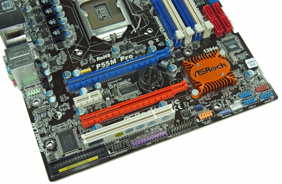
ASRock includes two PCIe x16 slots (x16 operation for the first slot, x4 operation for the second slot), one PCIe x1 slot, and a single PCI slot. The PCIe x1 slot will be unavailable when utilizing a dual slot video card. The front panel header, three USB headers, IEEE 1394a header, and floppy drive connector are located at the edge of the board.
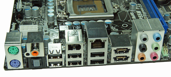
The I/O panel is full. We have six USB 2.0 ports (total of twelve on the board), PS/2 mouse and keyboards ports, dual eSATA/USB powered ports from the P55, IEEE 1394a port offered by the Via VT6330 chipset, Gigabit Ethernet LAN port via the Realtek RTL8111D chipset, optical out/coaxial out S/PDIF ports, and the audio panel that provides 8-channel audio output from the Via VT1708S HD audio codec.


Tech
ASRock also features lower ESR solid capacitors, lower RDS(on) MOSFETs, and high quality chokes on their entry level board. This board is also EuP ready and features ASRock’s Instant Boot technology. We think the board is extremely well built for a $100 design considering the average cost of a P55 motherboard is around $153.
DPC Latency
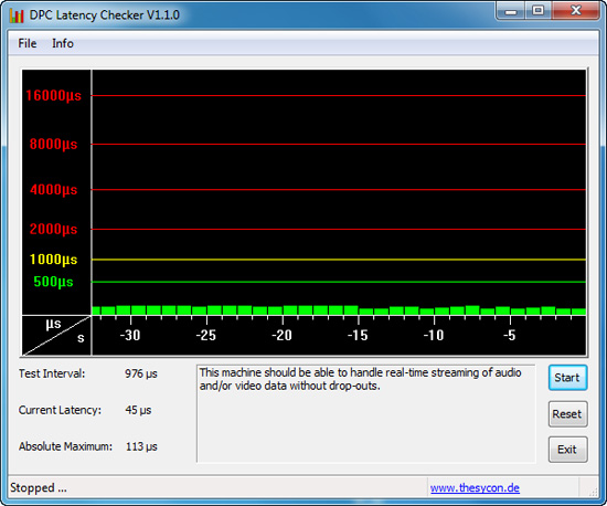
Our test used the Core i5/750
at stock settings with 8GB of memory installed with timings set to 6-6-6-18 at
DDR3-1333. The latency numbers for the ASRock board are lower and more consistent than the Gigabyte board.
Software
ASRock provides several software applications with the P55M Pro. We will take a quick look at their OC Tuner, Intelligent Energy Saver (IES), and OC DNA.
OC Tuner
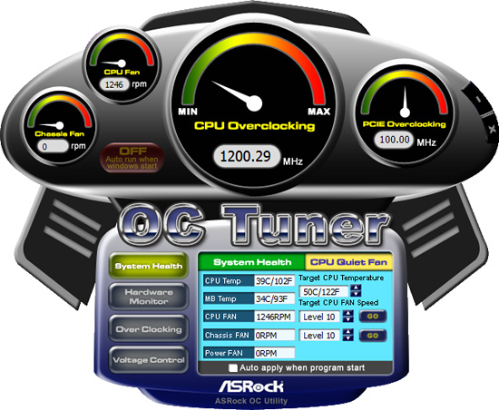
ASRock’s OC Tuner application provides health and hardware monitoring, voltage control, and overclocking capabilities. OC Tuner is actually a solid Window’s based overclocking and monitor tool. We still want the ability to save the settings to the BIOS in real time - or at least a BIOS profile setup more robust than the OC DNA tool below. The version shipped on the driver CD worked correctly, but we always suggest you keep the supplier’s utilities up to date.
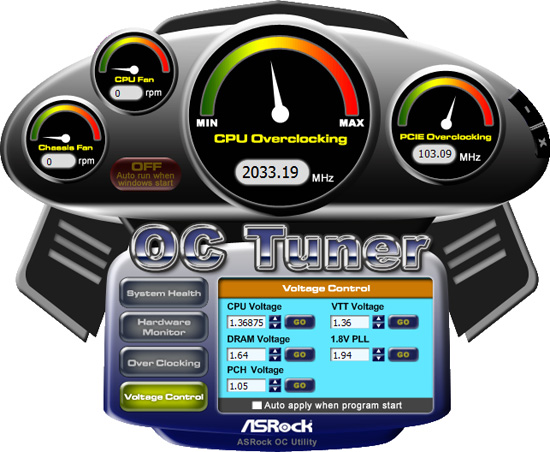
Sounding like a broken record, we still prefer to tune our system within the BIOS. However, this application is useful for extracting a decent amount of performance improvement out of the system after booting into Windows. We also found the capability to adjust the CPU and Chassis fan speeds to be handy during the overclocking tests.
OC DNA
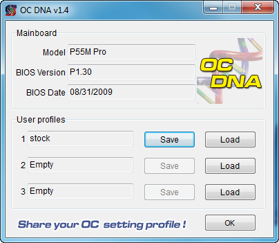
The OC DNA application allows you to save your OC profiles to the three provided user profiles within the BIOS. You can then load them from Windows (requires a reboot to set the profile) or share the OC profile with users of this board.
IES
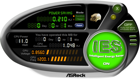
One of the most useful features from ASRock is their Intelligent Energy Saver (IES) power management solution. ASRock provides a Windows-based software application to control IES. After installing the software (we highly recommend downloading the latest version) and a quick reboot, the application is ready for use. The control panel is powered down by default and it is up to the user to turn it on with a simple click of the IES button. IES can also be enabled within the BIOS, doing this will disable Load Line Calibration (No Vdrop).
The IES software is simple to use and easy to understand. A provided power savings meter in the top portion informs the user of current and historical power savings information. Real-time CPU power usage is available along with the processor speed. We generally found the application would save around 4W at idle, and depending up the application in use, around 20W under load conditions that leads to superb results compared to other P55 boards.
Overclocking
If you are on a strict budget but still want a P55 motherboard with a full feature set that offers solid overclocking abilities, the ASRock P55M Pro is a very good choice.
Core i5/750 8GB Results
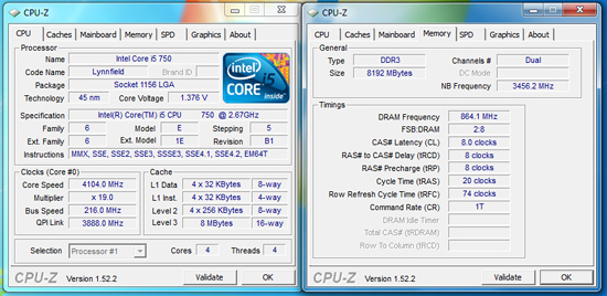
Our maximum stable overclock on air-cooling with the Core i5/750 resulted in a 4.1GHz clock speed at a respectable 216MHz Bclk with a variety of 8GB DDR3-2000+ kits. The primary voltages settings were 1.3625V VCore, 1.36V VTT, 1.80V PLL, and 1.64V VDimm. The VCore setting is deceiving. We had to run the board with Load Line Calibration (Vdrop off) enabled for stability. This was with setting the voltage manually to 1.3625V or with the Overdrive Offset enabled with +0.1625V.
This meant the VCore would rise to 1.384V~1.392V during load conditions. It was either this or run the processor at 1.425Vand accept Vdroop of 0.05V. Also, we had to relax memory timings to DDR3-1728 at 8-8-8-20 1T settings. VDimm would have to be increased to 1.71V (the next step from 1.64V) in order to run C7 settings on this board.
We could improve memory timings or speed with the Bclk set to 215 and dropping our CPU multiplier to 19, but that required a VCore increase to 1.375V as we left VTT at 1.36V along with enabling Vdrop in the BIOS. Memory had to be increased to 1.71V for C7 operation and PLL remained at 1.80V. We could run the memory at DDR3-2152 at 9-9-9-27 2T but VTT had to be increased to the next step at 1.42V and PLL to 1.94V. Performance was not measurably different from our 19x206 setting in application testing, but CPU temperatures were up 3C. Even though these settings passed our stability test suite, we just felt like the trade off in increased voltages was not worth some very minor memory performance gains.
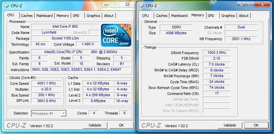
Core i7/860 8GB Results
Our i7/860 fared better clocking wise than the i5/750, but we could not match the 21x205 speeds generated with the Gigabyte board without raising VCore to 1.425V. We ended up at a perfectly stable 20x205 setting resulting in a 4.1GHz clock speed with 8GB at DDR3-1740 at 7-7-7-24 1T timings. However, our voltage settings were lower due to the decreased clock/memory speeds.
VTT is set to 1.36V, PLL at 1.94V, VDimm at 1.64V, and VCore at 1.350V with the Overdrive Offset/VDrop enabled. Under load conditions VCore was +.015V~+.02V with Vdrop enabled and -.055V~-.06V with it disabled. Our Core i7/870 clocks matched these exactly.
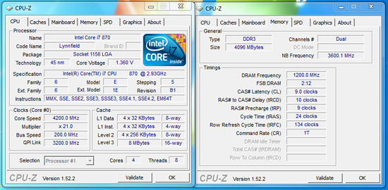
Core i7/860 4GB DDR3-2400 Results
ASRock advertised DDR3-2400 speeds so we decided to verify their claim. Unfortunately, the board had serious problem running our OCZ DDR3-2400 Blade kit at 2400 with the stock 9-10-9-24 1T settings on 1.71V. We just could not dial in stability at that memory speed. We had to settle for DDR3-2000 7-8-7-24 1T timings at 1.64V. Of course, those memory speeds is more than fast enough for application usage and let’s face it, nobody will be buying this board thinking they are going to break world records.


Thoughts
The overclocking results are solid and certainly 4.1GHz speeds are fast enough for most. Let’s face it; if you have to have the best possible OC performance, then the Gigabyte UD2 board is simply better. We have no concerns recommending the ASRock board for 24/7 overclocking use. When it is overclocked, the board is very stable. As a bonus, it had no problems doing an S3 resume with the Bclk set to 215.
In regards to voltage regulation, ASRock follows Intel’s guidelines exactly. This has advantages as the processor is always running at specifications when it comes to Vdrop and Vdroop, but the disadvantage is that one has to really take time to tune the board to get the most out of it. The board was really designed to get you to about 90% of your component’s capabilities and that is it. Trying to tune another 5% performance improvement was possible, but very time consuming and frustrating to be honest.
In most cases I would not use the word frustrating, but compared to the Gigabyte UD2 board, that next five percent in tuning consumed about five times as much time on the ASRock board and we still did not match the speeds on the Gigabyte board. Granted, we are talking about numbers that look really good in screenshots and yes, application performance like encoding and file compression will show a small improvement. However, one has to ask if it is worth it.
The end story is that we would rather implement a practical overclock around 3.8GHz with the i7/860 or i5/750 at 1.275V than push to speeds around 4.1GHz~4.3GHz that require more expensive memory kits and cooling. In that context, the ASRock board is more than capable for most overclocking duties.
Test Setup -
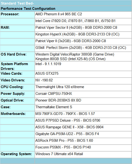
We utilized a wide variety of memory kits from Corsair, OCZ, Patriot, GSkill, Kingston, and Super Talent to verify memory compatibility on our test boards. Our OS and primary applications were loaded on the Kingston 80GB SSD drive and our games were operated off the WD 300GB VRaptor drive. We did a clean install of the OS and applications for each motherboard.
We chose the ASUS GTX275 video card and Corsair’s 750HX power supply. Yes, a 750W power supply is overkill for our micro-ATX boards, but will be required when we test CF/SLI in future P55 reviews. The difference in power consumption was under 1.5W on average between the 750HX and 520HX power supply.
Our air cooler of choice is Thermalright’s Ultra 120 eXtreme, primarily for its exceptional performance during our overclocking tests. We also tested with the retail cooler and those results along with direct CPU comparisons can be found here.
We are providing initial test results with Foxconn’s P55MX. Our test sample had an early revision P55 chipset and the retail board just arrived. Our application and game benchmarks are with the retail board. The board is limited to 4GB of memory in our tests due to the dual slot design. Our multitask test had two applications removed to bring the memory required footprint down to 3.82GB. An article update will be generated once we complete our overclocking and stability tests. This board sells for around $90 and is really designed for the business or SOHO user.
Our 790FX/X58 results are provided for comparison only. For our test results we setup each board as closely as possible in regards to memory timings. Otherwise all other settings are left on auto. The P55 and 790FX motherboards utilized 8GB of DDR3, while the X58 platform contained 6GB. The P55 and X58 DDR3 timings were set to 7-7-7-20 1T at DDR3-1600 for the i7/920, i7/870, and i7/860 processors at both stock and overclocked CPU settings.
We used DDR3-1333 6-6-6-18 1T timings for the i5/750 stock setup as DDR3-1600 is not natively supported in current BIOS releases for this processor at a stock Bclk setting of 133. We had early BIOS releases that offered the native 1600 setting but stability was a serious problem and support was pulled for the time being. Performance is essentially the same between the two settings.
The AMD 790FX setup is slightly different as trying to run DDR3-1600 at CAS 7 timings on the 1:4 divider is extremely difficult. DDR3-1600 is not natively supported on the Phenom II series so this divider is provided with a caveat that you are overclocking the memory bus. The same holds true for the Lynnfield (i7/8xx, i5/7xx) processors as DDR3-1333 is officially the highest memory speed supported and it is DDR3-1066 for the Bloomfield (i7/9xx).
Without resorting to some serious overvolting and relaxing of sub-timings, we set our AMD board up at DDR3-1600 8-8-8-20 1T timings. The difference in performance between C7 and C8 DDR3-1600 is practically immeasurable in applications and games on this platform. You might pick up an additional few tenths of second in SuperPi or a couple of extra points in AquaMark or 3DMark 2001SE, but otherwise performance is about equal.
However, in order to satisfy some of our more enthusiastic AMD supporters, we also increased our Northbridge speed from 2000MHz to 2200MHz to equalize, if not improve, our memory performance on the AMD system. Yes, we know, further increasing the NB speed will certainly result in additional performance but the focus of this short article is to show clock for clock results at like settings. Personally, I would run DDR3-1333 C6 with 8GB as this platform favors tighter timings over pure bandwidth.
We will provide P45/Q9550 platform results in the next roundup.
I know what you did last BIOS release...
One problem we constantly ran across in early testing and major reason why we delayed the start of these roundups was the floating Bclk problem. Motherboard suppliers have tweaked FSB speeds for years in an attempt to squeeze out that last little bit of performance at stock speeds. Well, the same thought process went into a few of the P55 BIOS releases from several manufacturers.
Even though we manually set the Bclk rates to 133, a few of the boards decided to still float the Bclk rates up to 138 in some cases, 136 in others. If the manufacturer did not change their BIOS to lock Bclk rates at 133 when manually set to 133, then we set the boards to 132. That in its self caused a few quick BIOS updates and except for one upcoming board, we are no longer experiencing this problem.
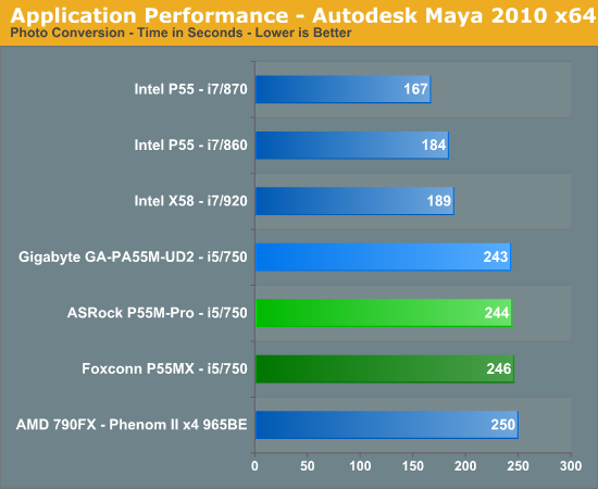
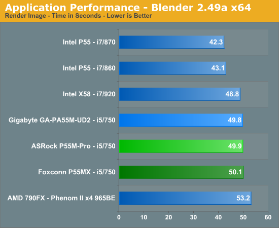
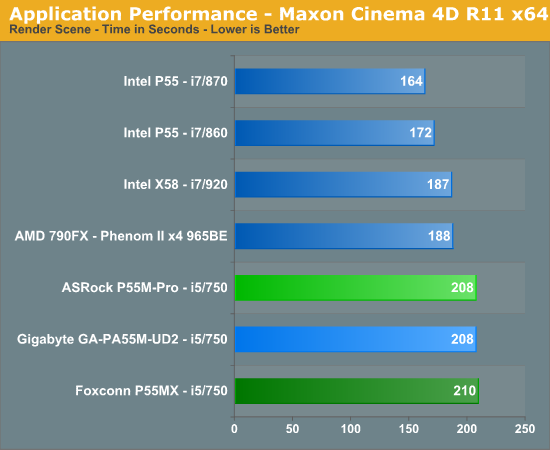
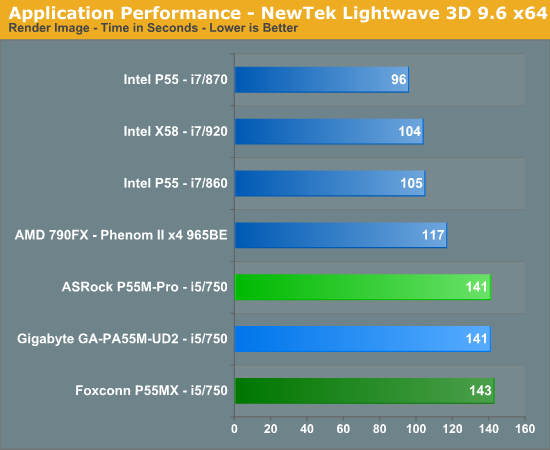
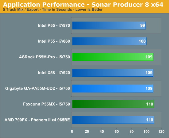
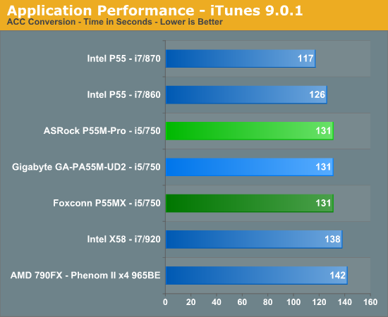
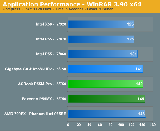
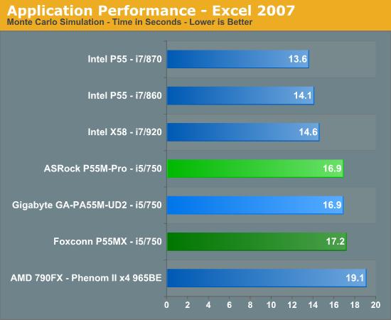
There's really no other way to say this: ASRock's P55M-Pro, Gigabyte's GA-PA55M-UD2 and Foxconn's P55MX all perform almost exactly the same in every single benchmark we ran.
Application tests, game tests, LAN tests, even USB, Firewire, and SATA controller performance was virtually identical across the board. We've known for a while now that motherboards of a given generation all perform the same, but there's honestly no more to it than that.
We've included a wealth of application, gaming and peripheral performance data for you to see for yourself, but honestly, it's not what's important when it comes to picking a micro-ATX P55 motherboard. Features, overclocking potential, support, and price point are what matter here.
The biggest difference between the boards, from a performance standpoint, actually surfaces in power consumption:
At
idle the Gigabyte GA-P55M-UD2 draws the least amount of power while under load, ASRock's P55M-Pro is absolutely stingy. It's not a huge margin, but big
enough to crown the Gigabyte board the least power hungry micro-ATX P55 board we've tested from an overall vantage point. We had to make sure that Enhanced Halt State (C1E) was enabled on the ASRock board along with ACPI Suspend (S3) was set to auto for all power management features to work correctly. If you happen to be using an SSD drive, then the Check Ready Bit option must be disabled on the ASRock BIOS (AMI in general) or the system might not resume correctly from S3. Otherwise, S3 resume worked properly on both boards at stock and overclocked settings.
Application/Gaming Performance
We're presenting all of the application/gaming performance data without commentary because, as we mentioned before - there's no real appreciable performance difference between these three boards. All of the boards were run with the Core i5 750 and we've included the Phenom II X4 965 BE as well as the i7 860, 870 and 920 purely for reference. Please check our Lynnfield launch article to see how well this processor performs against a variety of CPUs.
In many of our tests, the Core i5 750 is the same speed or faster than the Phenom II X4 965 BE. The lack of Hyper Threading prevents it from being a runaway success. In other cases, the Phenom II X4 965 is faster - and by a large degree.
Intel was very careful to disable HT on the 750, without it, there would be no reason to spend the extra money on the Core i7 860. Just as it was with Bloomfield, $284 is the sweet spot for Lynnfield if absolute performance is a requirement. Now for the benchmarks.
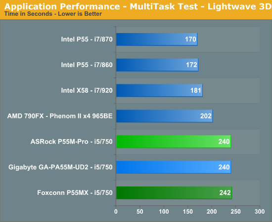
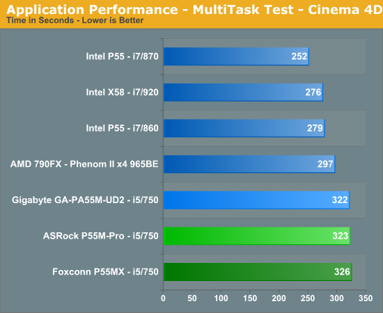
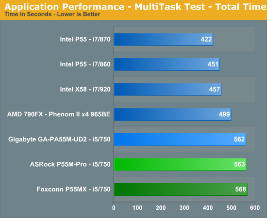
Multitasking-
The vast majority of our benchmarks are single task events that utilize anywhere from 23MB up to 1.4GB of memory space during the course of the benchmark. Obviously, this is not enough to fully stress test our 6GB or 8GB memory configurations. We devised a benchmark that would simulate a typical home workstation and consume as much of the 6GB/8GB as possible without crashing the machine.
We start by opening two instances of Internet Explorer 8.0 each with six tabs opened to flash intensive websites followed by Adobe Reader 9.1 with a rather large PDF document open, and iTunes 8 blaring the music selection of the day loudly. We then open two instances of Lightwave 3D 9.6 with our standard animation, Cinema 4D R11 with the benchmark scene, Microsoft Excel and Word 2007 with large documents, and finally Photoshop CS4 x64 with our test image.
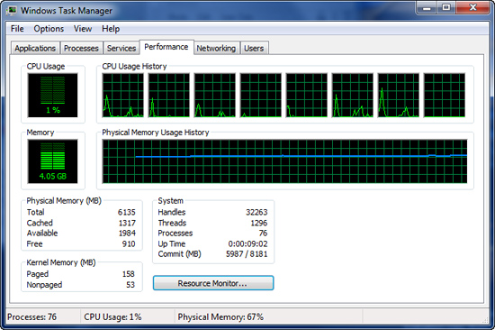
Before we start the benchmark process, our idle state memory usage is 4.05GB.
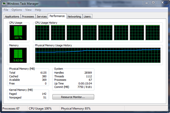
We wait two minutes for system activities to idle and then start playing Pinball Wizard via iTunes, start the render scene process in Cinema 4D R11, start a resize of our Photoshop image, and finally the render frame benchmark in Lightwave 3D. Our maximum memory usage during the benchmark is 5.62GB with 100% CPU utilization across all four or eight threads.
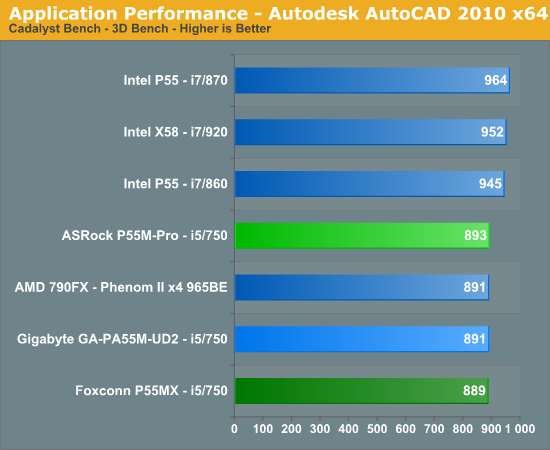
AutoCAD 2009 x64
We utilize AutoCAD 2010 x64 and the Cadalyst Labs 5 benchmark.
3ds Max 2010 x64
We utilize a rather large mental ray image and track the time it takes to render it.
Blender 2.49a x64
We utilize the flying squirrel benchmark image and track the time it takes to render it.
Cinema 4D R11 x64
Cinema 4D R11 is one of our favorite programs to create high-end 3D images and animations. We track the time it takes to render a swimming pool layout.
LightWave 3D 9.6 x64
Another popular 3D rendering program is Lightwave 3D 9.6. In this test we time the rendering of a single frame from an office building animation. The time to render the full scene is approximately four and a half hours.
Video
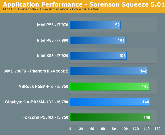
Sorenson Squeeze 5.01
We are using Sorenson Squeeze to convert eight AVCHD videos into HD Flash videos for use on websites.
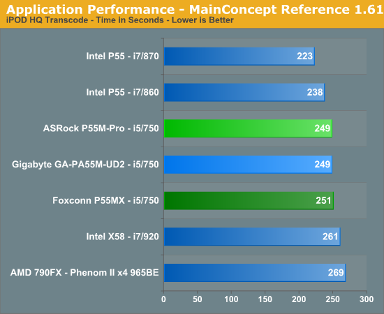
MainConcept Reference 1.61
One of our favorite video transcoding utilities is MainConcept Reference. We set our profile to iPOD HQ NTSC and then transcode a 651MB 1080P file to a iPOD friendly 34.7MB file.
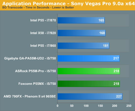
Sony Vegas Pro 9.0 x64
We transcode a 370MB 1080AVCHD file using the Mainconcept MPEG-2 1920x1080 60i, 25Mbps setting with 6-channel audio.
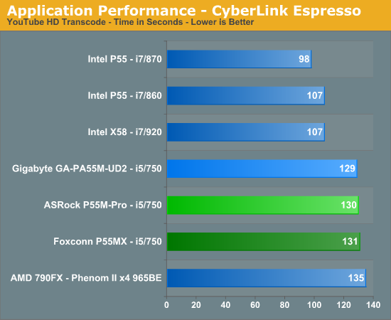
CyberLink MediaShow Espresso
We transcode a 370MB 1080AVCHD file into a HD friendly file suitable for publishing on YouTube. This program features GPU hardware accelerated decoding via ATI Stream or NVIDIA CUDA but is disabled in our test routines.
Audio
Sonar Producer 8 x64
We utilize Sonar Producer extensively at home when mixing various music tracks. This test performs a complex mix of five individual tracks into a single title. We covert these tracks into a WAV format utilizing a 192kHz sample rate along with all other options enabled. This title thrives on memory bandwidth.
iTunes 9 x64
We import the album Tommy by The Who to our disk in WAV format. The directory consists of 25 songs totaling 751MB. We then convert this music collection to MP3 format utilizing 320Kbps VBR Highest audio settings or to an AAC format using the iTune Plus option.
WinRAR 3.9 x64
This benchmark compresses our AT workload consisting of a main folder that contains 954MB of files in 15 subfolders. The result is a file approximately 829MB in size.
Microsoft Excel 2007 SP1
Excel can be a very powerful mathematical tool. In this benchmark, we are running a large Monte Carlo simulation on stock pricing data to estimate the riskiness of an investment portfolio.
Adobe Lightroom 2.4 x64
Lightroom is a quick and easy to use program for batch conversions on digital photos. We perform a standard conversion of 50 RAW images into the JPEG format.
Bibble 5.0
We utilize Bibble Labs’ Bibble 5 v2 to convert 50 RAW image files into full size JPEG images with the program’s default settings. This program is fully multithreaded and multi-core aware.
Windows Live Movie Maker
We utilize our standard HD video file, add music, and start/ending transition effects.
FarCry 2
Featuring fantastic visuals courtesy of the Dunia Engine, this game also features one of the most impressive benchmark tools we have seen in a PC game. We set the performance feature set to Very High, graphics to High, and enable DX10 with AA set to 2x. The in-game benchmark tool is utilized with the Ranch Small level and we report an average of three test runs.
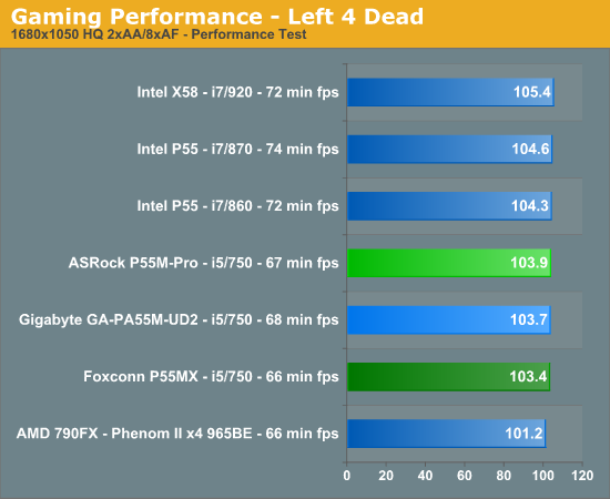
Left 4 Dead
This game is a blast and addictive to boot - provided you like killing hundreds of zombies while trying to take care of your teammates and sustaining high blood pressure rates. We enable all options, set AA to 2x and AF to 8x, and play back a custom demo of a game session from the Runway Finale chapter within the Dead Air campaign.
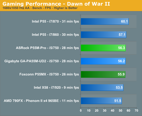
Warhammer 40K: Dawn of War II
We are big fans of the Warhammer franchise, especially Dawn of War II. One of the latest RTS games in our library is also one of the more demanding titles on both the CPU and GPU. We crank all options to High, enable AA, and then run the built-in performance benchmark for our result.
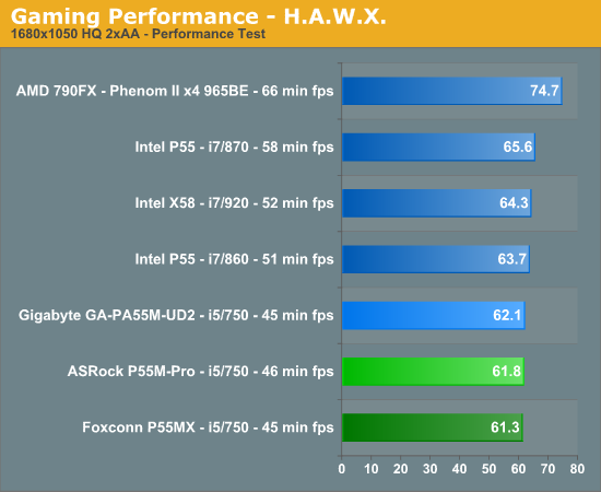
Tom Clancy's H.A.W.X.
While not a true flight simulation or even serious air combat game, it is a lot of fun and looks visually stunning on a 30” monitor with all options turned up. In our case, we set all options to high, enable 2xAA and DX10, and then use FRAPS to time a custom demo sequence. We run three loops of the benchmark and average our scores for the results.
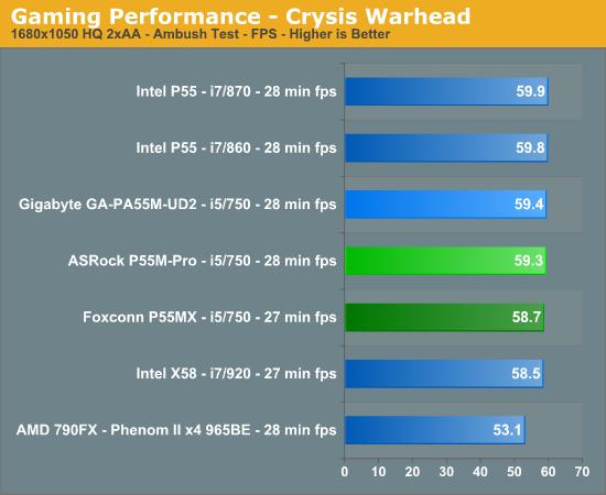
Crysis Warhead
We utilize the Ambush level for our game test. We set the resolution to 1680x1050 with 2xAA, DX10, and 64-bit enabled.
Networking
The Windows 2000 Driver Development Kit (DDK) includes a useful LAN testing utility called NTttcp. We used the NTttcp tool to test Ethernet throughput and the CPU utilization of the various Ethernet Controllers used on the Intel motherboards. We set up one machine as the server; in this test, an Intel system with an Intel CSA Gigabit LAN connection. Intel CSA has a reputation for providing fast throughput and is a logical choice for our Gigabit LAN server.
On the server side, we used the following Command Line as suggested by the VIA whitepaper on LAN testing:
Ntttcpr -m 4,0,‹server IP› -a 4 -l 256000 -n 30000
On the client side (the motherboard under test), we used the following Command Line:
Ntttcps -m 4,0,‹client IP› -a 4 -l 256000 -n 30000
At the conclusion of the test, we captured the throughput and CPU utilization figures from the client screen.
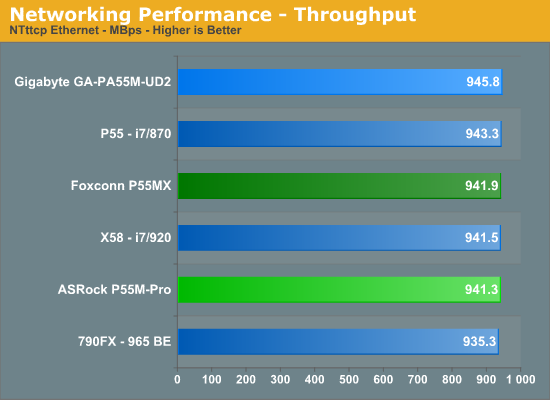
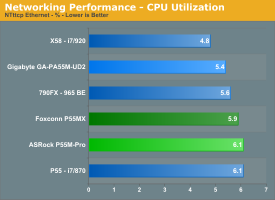
Our network throughput test indicates how well a particular controller design from Realtek, Marvell, or Intel performs instead of being indicative of true chipset performance. This also holds true for the CPU utilization results, though this test can also be influenced to certain degree by the BIOS code and chipset interconnect design.
The CPU utilization and throughput numbers favor the Realtek controller on the Gigabyte board, followed closely by the same Realtek chipset on the Foxconn and ASRock boards. In practice, few if any users will notice a difference, even if they have the requisite gigabit hub, as storage performance frequently bottlenecks the actual transfer rates.
For our second series of networking tests we utilize a Promise SmartStor NS4600 NAS unit equipped with two WD Caviar Black 640GB drives in RAID 1 operation. We are using two benchmarks from Intel’s popular NASPT 1.70 testing tool. The Promise NAS unit is connected to each test platform via a NetGear Gigabit Ethernet switch. We left all settings at their defaults on both the motherboard and Promise NAS unit. Our was to maximize the performance of the NAS unit to verify our network throughput capabilities on each motherboard.
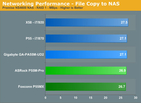
Our three P55 test subjects perform almost identically in our actual usage tests.
USB / FireWire Performance
Our USB transfer speed tests are conducted with an USB 2.0/FireWire based Lacie external hard drive unit featuring a 1TB 7200rpm Samsung drive . In the SSD to External test, we transfer a 3.82GB folder containing 2735 files of various sizes from our Kingston 80GB SSD to the Lacie drive. In the next two file tests, we use the same 3.82GB folder to transfer from our WD VRaptor 300GB hard drive to the external Lacie drive utilizing the USB 2.0 and IEEE 1394a interface.
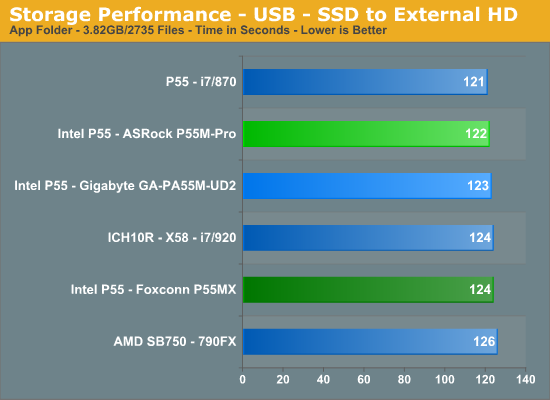
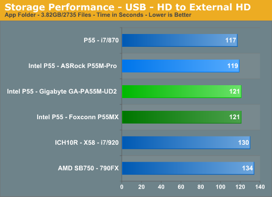
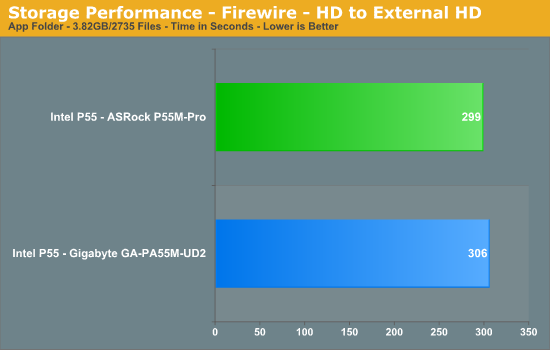
The ASRock board slightly outperforms the Gigabyte board in our USB transfer tests. The VIA Firewire controller on the ASRock board has a slightly higher write speed (+3Mb/s) under HDTach/HDTune and it shows up in our file transfer test.
Storage Performance
In our storage test, we utilize the same 3.82GB test folder and transfer it from our WD VRaptor drive to our Kingston 80GB SSD.
Once again, our P55 motherboards perform almost identically. The P55 chipset on the Gigabyte board has a 3% advantage over the JMicron controller on the same board. However, any measurable differences were not recognized in actual usage.
Audio-
We are planning on taking an in-depth look at all of the current on-board audio codecs and compare them to a couple of discrete audio cards from ASUS and AuzenTech in the near future. In the meantime, we will provide a quick overview of the control panels from the two competing solutions today and a quick subjective analysis.
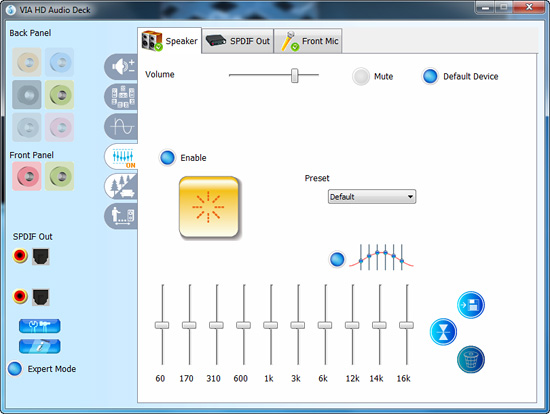
ASRock utilizes the VIA VT1708S 8-channel audio codec on the P55M Pro motherboard. To be honest, I had low expectations of this particular chipset. In actuality, it is a decent competitor to the Realtek ALC 888B utilized by Gigabyte. In fact, VIA has made great progress in their driver set and at this point I firmly believe the actual implementation by the motherboard manufacturer in regards to shielding is more important to audio quality than the any potential differences between the two chipsets.
That said, VIA has a very good control panel and option setup, certainly more so than Realtek in this particular case. The most beneficial item is the equalizer as you will need it for music playback. Midrange performance on this chipset is lacking depth and highs at times sound tinny. Both chipsets scored about even in Rightmark’s excellent Audio Analyzer software test suite with THD+ numbers slightly favoring the Realtek solution.
Unfortunately, my ears thought the difference in quality between the two solutions was a bit greater. The main problem with the VIA solution as implemented by ASRock was background noise that was directly attributable to electrical shielding problems on the board. In headphone mode, I could hear a slight background hum that would rise and fall with load activity on both the CPU and storage subsystems. It was very slight, but just enough to be noticeable in several classical and jazz soundtracks. It was also present in several games, mainly simulations and RTS games where there is not constant gunfire present in most first person shooters.


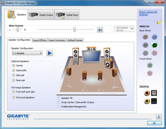
Gigabyte utilizes the Realtek ALC 888B 8-channel audio codec on the P55M Pro motherboard. Audio quality in music was better than the VIA VT1708S thanks to clearer midranges, but highs were still leaned on the tinny side and bass was even between the two chipsets.
Otherwise, I preferred the Via solution in games and movie playback, not by much, but channel separation was slightly better. Of course, if you really want better analog output a good discrete audio card is the solution. For most of us, either of the audio solutions will suffice, but thanks to the lack of background noise, we will have to give the Gigabyte board the win here.


The Dark Side of the P55
So you just purchased a Core i5/750 or i7/860 along with a new P55 motherboard and DDR3 memory kit. Congratulations on your new arrival and hopefully it will provide years of trouble free operation or at least a few months until the latest greatest item hits the market. However, if you notice a few gremlins causing havoc with your system, as they are wont to do at times, then we possibly have good news for you. We have compiled a short list of problems that reared their head during testing and will be discussing the primary problem today and others as we continue our P55 articles.
The Great Heist
One of the most irritating problems we ran across during testing was playing “Where’s Waldo” with our memory configurations. Our standard P55 test bed is equipped with 8GB of memory. We started noticing weird memory benchmark results in Everest that just did not make sense as Read/Write rates were up 30% lower than our 4GB setup on the same board or other 8GB configurations. These along with applications like Photoshop CS4 x64 and AutoCad 2010 x64 refusing to recognize up to 4GB of memory had us searching for answers.
A look at the BIOS indicated 8GB was indeed available and applications from Everest to CPU-Z along with the suppliers own tuning tools indicated no problems. So we turned to Performance Monitor in Windows 7 to solve our dilemma. Sure, enough, in every case we would only see 4080MB~4096MB listed as available memory. We dug deeper in Resource Monitor and found that the BIOS hard reserved around 4.1GB of memory and it was not available to the OS. We also ran across the same problem on a few boards with 4GB of memory installed.
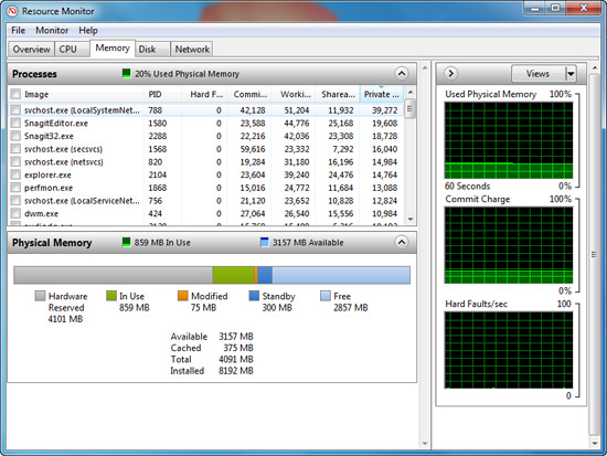
There are several reasons for this occurring. The primary reason is that the motherboard supplier did not program the BIOS correctly to automatically remap memory above the 4GB mark. In the AMI BIOS’ utilized by ASUS and ASRock, among others, there is a Memory Remapping option in the BIOS setup screen that needs to be enabled on early BIOS releases. Later BIOS releases automatically enable this feature if more than 4GB of memory is detected at POST. So the recommended solution is to update your BIOS to the latest release if this is a problem in your system.
That said, even after a round of BIOS updates from all the suppliers, we still had this problem occurring, just not as often. It also turns out that high Bclks with 8GB of memory installed will also trigger the problem. Even with memory remapping properly enabled, there is a chance this problem will still occur. Depending on the BIOS, it will simply ignore the additional two channels and continue to POST or it will not POST at all.
This problem depends on a Holy Trinity combination Memory, Motherboard, and Processor quality. If the board does not recognize the memory SPD correctly or if the SPD is wrong, it can happen, but primarily it seems to be processor or motherboard related. On the processor side, it seems especially prevalent with the i5/750 as the IMC tends to have trouble handling high memory clocks above 2100 with 8GB installed, it is not impossible, but our first retail samples are not fairing very well.
Why the i5/750? Mainly because of binning as our 860 would clock up to 2150 before problems arose and the 870 would hit 2200. Of course, this is a rare situation as anyone buying this platform would probably not spend $400 on high-end memory and overclock it at these levels. But, with us trying to find the practical limits on each board, it did cause a headache or two.
The primary problem is with the motherboard design. The majority of the P55 motherboards are built on either a 4-layer or 6-layer design. The 6-layer design has (obviously) to additional layers that can be utilized for electrical routing. On a 4-layer design, Channel A memory signal and clock signal are placed on the top layer and Channel B is placed on the bottom layer. In a 6-layer design, half of Channel A is placed on the top layer and other half on the bottom layer. Half of channel B is placed on inner layer 1 and the other half on inner layer 2. This significantly reduces crosstalk between each data Group. As such, the memory capabilities of the 6-layer board will greatly improve 8GB memory clocking above 2000MHz.
Once again, make sure you are on the latest BIOS and considering the early nature of this platform, stay current with a stable release for the next couple of months as any remaining bugs are squashed.
Quick Thoughts-
We normally wait until the end of a roundup to determine our awards. However, after testing close to twenty P55 motherboards, we have a very good idea of those that deserve awards and those that will either be recommended or not. The ASRock P55M Pro is a recommended board, especially given the feature set and price. However, it ran smack into a buzz saw today from Gigabyte. ASRock has nothing to be ashamed of (their Extreme board is terrific) as this Tasmanian Devil will put a lot of P55 boards to shame when one considers its overclocking potential, feature set, quality, performance, and price.
Gigabyte has faithfully produced a board that we believe was the original intent of the P55 platform when Intel designed the platform. A platform that should stand for simplicity, low cost, and great performance from Intel's latest generation technology. True, the P55 will never match the X58 in pure performance potential, but that was not its intended mission. Instead, it was meant to deliver Nehalem technology to the masses at an affordable price point. It is almost at that point, especially with Clarkdale coming soon, except we still think the i5/750 should be priced lower, maybe in the $169 range in order to make an upgrade from the current Core 2 Quad series an almost given.
That said, based on price to performance ratios, the i5/750 is a great value in the midrange performance market at $199. What makes it even more attractive is having a motherboard that offers a full feature set, high-quality components, and performance to back it up at the $100 mark. While no longer a $100 board, the Gigabyte GA-P55M-UD2 meets just about everyone of those targets. For an entry level motherboard, it features a very good micro-ATX layout, quality components, great BIOS, superb overclocking capabilities, and a price that almost belies its feature set and performance. There are many things to like about this board but we think the price to performance ratio is just terrific.
The BIOS has just the right amount of options to allow excellent overclocking capabilities while retaining enough simplicity that a beginner can quickly overclock just utilizing the auto settings. The BIOS design and information provided is a vast improvement over previous Gigabyte designs in the price sector. As good as the board is we still think the limited amount of fan headers (two) is an inexcusable mistake and the BIOS could use additional information like stock voltage settings for each option.
Award
 |
We are honored to present our Gold Editors' Choice award to GIGABYTE for their impressive GA-P55M-UD2. What we find truly amazing about this motherboard is that it was never intended for full release into the retail market. It was meant for limited channel distribution and OEM kits. Gigabyte was sitting on a gem of a board and had no idea just how capable it was at first glance. Sometimes you cannot judge a board by its price. This board features Gigabyte's Ultra Durable 3 technology, impressive overclocking capabilities for an entry-level board, excellent stability and compatibility, along with being consistently at or near the top of our benchmarks. It ultimately offered the best overall value we have seen in this market segment and for that it receives our highest accolades.
There is no perfect motherboard and probably never will be one. The GA-P55M-UD2 is certainly not perfect, but it meets its goal at a price point that makes us wonder about spending $250 on a P55 motherboard. Granted, there are boards in the $200 range that will also receive our accolades, primarily based on technical merit. The UD2 board does have a couple of flaws. The lack of more than two fan headers is perplexing at best and it tended to be picky with memory until the F4 BIOS release.
Also, one of its strengths is a weakness, that being a micro-ATX form factor product. Although Gigabyte did a really good job with the layout, things are cramped and having the memory installed along with all storage cables run is a wise move to make before installing the video card. One other factor is that this board features a 4+1 PWM setup that is not designed for high voltage overclocking. It overclocks very well but there is a limit to current draw if you were thinking about using the board for more extreme overclocking testing. Instead, recognize its limits (no more than 1.45V) and all will be fine or purchase a board designed with this type of overclocking in mind.
GIGABYTE has come a long way in improving their customer support, website information, technical documentation, and warranty support compared to our experiences over a year ago. We would still like to see them take a more interactive customer support role in the same way that EVGA supports their customers. The current help ticket system is just not user friendly, nor does it provide a quick answer to potential problems. While these problems do detract from the product and company, overall this board is one of the better values in the P55 family.


