Original Link: https://www.anandtech.com/show/1177
Gigabyte K8NNXP-940: Built on Athlon64 FX51 Strengths
by Wesley Fink on October 9, 2003 11:52 PM EST- Posted in
- Motherboards
Things were quite strange in the month before the Athlon64 launch. That was about the time reviewers received first details of FX51 — the Enthusiast version of Athlon64. For those who had been following AMD's slow progress to A64 launch, it certainly looked like AMD was worried and wanted to make absolutely sure that A64 would outperform anything Intel could throw at the launch. Perhaps the EE chip info leaked to AMD, and the FX was the insurance just to make CERTAIN Athlon64 would maintain a performance lead. Perhaps AMD was concerned that lack of Dual-Channel memory support on Athlon64 might make consumers think A64 was a slower chip. It isn't, but perceptions sometimes matter more than facts. We don't know the real reason for the FX launch, but whatever the reason, it is clear that it was a last minute decision.
FX51 is basically an Opteron with a different name. It works with a BIOS update on many Socket 940 Opteron boards, and will not work on any of the Socket 754 boards being introduced right now. Like Opteron, it also suffers (or benefits, depending on your perspective) from the requirement for Registered Dual-Channel memory to operate. The only concession is that while it can use Registered ECC memory like Opteron, only Registered is required on FX51.
The even stranger part was AMD's positioning of FX51. They refused to even sample Athlon64 chips, forcing review sites into a position of begging their Advertisers for Athlon64 chips to review anything. Athlon64 launch partners were frustrated because many review sites could not review their new boards because they had no Athlon64 chips. The only sampling that was done by AMD was the very limited sampling of FX51 chips in an AMD prepared system. AMD was clear in their actions and words that they wanted the Launch to be with Athlon64 FX51 processors.
Even now, we have to wonder why. Athlon64 is fully competitive with Pentium4 3.2GHz. It enjoys both a price advantage over the P4 3.2 and the Athlon64 FX51, and, maybe even more important to buyers, it is available while there are almost no FX51 chips to be found. There were also many, many Athlon64 boards at launch, and only the Asus SK-8N board for the FX51 — a board first released as an Opteron motherboard. In addition, AMD was clear in its plan to move FX51 as quickly as possible to Socket 939 in 2004, which is capable of using regular unbuffered memory like most enthusiasts already own. AMD also announced very small production numbers for Socket 940 FX, leaving little incentive for manufacturers to produce Socket 940 boards for the desktop.
Thankfully, the major players — like Gigabyte, Asus, and MSI – have delivered or will deliver Athlon64 FX boards. We were glad to see Gigabyte's K8NNXP-940, which continues Gigabyte's recent stretch of high-end “Dual-Miracle” motherboards. The name is the same as Gigabyte's nForce3 Athlon64 board, with the addition of “940” to the name. As you will see, however, the differences are much deeper than just a different socket.
Gigabyte K8NNXP-940: Basic Features
| Motherboard Specifications | |
| CPU Interface | Socket-940 Athlon64 FX |
| Chipset | nForce3-150 Single-Chip |
| Bus Speeds | 200MHz to 300MHz (in 1MHz increments) |
| PCI/AGP Speeds | Auto (Variable) or Fixed 66-100MHz (in 1 MHz increments) |
| Available CPU Ratios | Auto, 4X to 25X in 0.5 increments |
| Core Voltage | Normal, 0.80V to 1.70V in 0.025v increments |
| DRAM Voltage | Normal, +.1, +.2, +.3V |
| Chipset (VDDQ) Voltage | Normal, +.1, +.2, +.3V |
| Hypertransport (VCC12_HT) Voltage | Normal, +.1, +.2, +.3V |
| Memory Slots | Four 184-pin DDR DIMM Slots Dual-Channel Configuration For Registered/Registered ECC |
| Expansion Slots | 1 AGP 8X Slot 5 PCI Slots |
| Onboard Serial ATA RAID | Silicon Image Sil3112 supports Raid0/1 |
| Onboard IDE RAID | Two Standard ATA133/100/66 Plus 2 GigaRAID ATA133 IDE RAID |
| Onboard USB 2.0/IEEE-1394 | Six USB 2.0 ports supported by nF3 TI 1394B (800 Mb/s) FireWire (2 ports) |
| Onboard LAN | Two ports, Realtek Gigabit LAN + Realtek 10/100 LAN |
| Onboard Audio | Realtek ALC658 codec AC '97 2.3 6-Channel with UA |
| BIOS Revision | F1 Release 7/22/2003 |
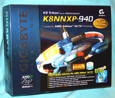
The Gigabyte K8NNXP-940 is Gigabyte's top board for the Athlon64 Enthusiast, and the fancy embossed foil packaging tries to convey that. This is typical of recent Gigabyte top-line boards.
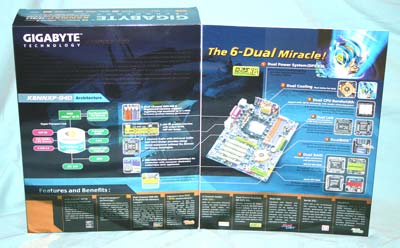
Gigabyte continues the recent “6-Dual Miracle” theme with the K8NNXP-940, with the Dual 32-bit/64-bit Dual CPU bandwidth replacing Hyperthreading as Athlon64's Dual. As the flagship for the Gigabyte AMD line, every feature you can imagine is lavished on the K8NNXP-940. The most significant new addition is 1394b Firewire. This is the first board that we have tested with the new 800Mb/s firewire.
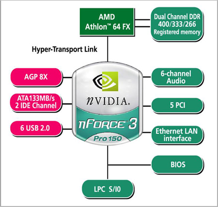
Gigabyte uses the nVidia nForce3-Pro150 single-chip solution on the K8NNXP-940. While the nF3-150 and nF3-Pro150 are currently limited to 600MHz HyperTransport, communication to the FX processor is direct and not bottlenecked by slower speed chip communications in traditional north/south bridge chipsets. The nF3-150 is used on motherboards designed for the single-channel Socket 754 Athlon64, while the nF3-PRO150 is designed for the Dual-Channel Opteron or Socket 940 FX51.
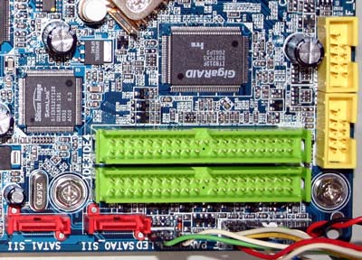
The Gigabyte uses both the GigaRAID IDE RAID based on the IT8212 chip and SATA RAID based on the well-regarded Silicon Image 3112/3512 chip. IDE RAID 0, 1, 0+1 are supported, and SATA RAID 0, 1. A full assortment of SATA/IDE cables and SATA/Molex power connectors are provided for drive hookup.
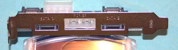
This includes Gigabytes unique external SATA bracket that allows connection of 2 external Serial ATA devices.
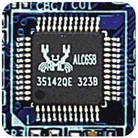
K8NNXP-940 uses the newest and best version of the Realtek audio codec called ALC658. This audio chips features Dolby Digital 6-channel sound and UAJ or Universal Audio Jack. This allows automatic jack programming as we've seen on some boards based on Intel's 865/875 chipsets.
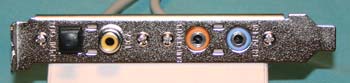
If you have Dolby digital capabilities, SPDIF output is provided by an included SPDIF bracket. SPDIF out jacks are provided for both optical and coaxial connections, as well as the 2 additional jacks for rear speakers in a powered 4 to 6 speaker arrangement. This allows rear speakers/subcenter to be used, while still leaving usable microphone and audio input capabilities. Many motherboards must program the rear-panel jacks and use the mic and input jacks for a 6-speaker setup. The ability to use six speakers, mic, and audio input is a nice feature — and more unique than you might imagine.
Realtek markets the ALC658 as a premium sound solution, and their first 2.3 compliant audio codec. The ALC658 is:
The ALC658 has six 20-bit DAC channels, two pairs of stereo 18-bit ADC, and an AC'97 2.3 compatible six-channel audio CODEC designed for PC multimedia systems. The ALC658 incorporates proprietary converter technology to achieve 100dB sound quality, meeting performance requirements on PC99/2001 systems and placing PC sound quality at the same level as consumer equipment.More information on the features and specifications of ALC658 is available at Realtek.
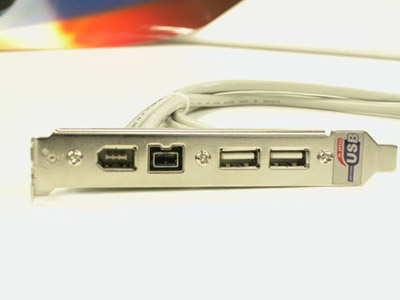
In addition to the 2 USB 2.0 ports on the rear I/O panel, Gigabyte provides an accessory bracket with two more USB 2.0 ports and 2-800mb/sec Firewire ports (one standard and one mini). An additional 2-port USB2.0 bracket is provided if needed. It is clear that the designers put some thought into this arrangement, since many users have front USB ports on their cases and the combo USB/firewire bracket may be their only added ports.
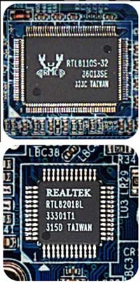
In keeping with the Dual theme, the K8NNXP-940 includes two LAN ports — a Gigabit LAN port and a 10/100 Ethernet port. Both chips are by Realtek.
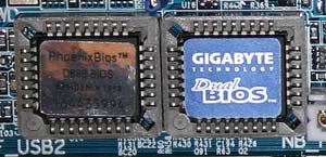
Gigabyte uses their trademark Dual BIOS on their mid- to high-end motherboards, and it is included on the K8NNXP-940. In addition to protection from a bad BIOS flash, the dual BIOS feature allows the creative end-user to set up 2 different BIOS setups for different OS or loads. In addition, the dual BIOS has hooks to allow direct flashing of the BIOS without an OS. You merely copy the BIOS file to a floppy, hit DEL during boot to enter BIOS, hit F8 to enter BIOS setup and make selections. Updating BIOS is as easy as it gets.
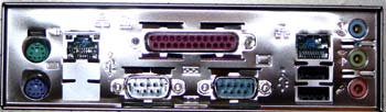
The K8NNXP I/O ports configuration is the assortment you will find on most high-end boards, and a custom ATX backplate is included.
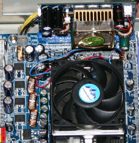
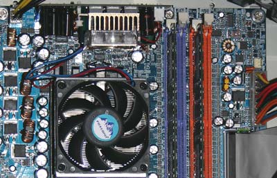
As part of their Dual Power and Dual Cooling features, Gigabyte includes the DPS-K8 power module. The base K8NNXP-940 is a 3-phase board, while adding the DPS-K8 module extends the board to 6-phase power and a second cooling fan. Gigabyte claims that the 6-phase power produces a more stable motherboard, better overclocking, and longer lasting components.
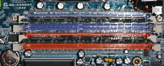
Four DIMM slots support Registered or Registered ECC Dual-Channel memory. Memory should be installed in matched pairs for Dual-Channel. Regular unbuffered DDR memory will not work in FX51 boards or in Opteron boards. Memory up to DDR400 is officially supported, which is an improvement over the DDR333 support that we have seen in past Opteron nForce3 boards.
Gigabyte K8NNXP-940: Board Layout
The Gigabyte has one of the best board layouts that you will find with few tradeoffs that can make installation more difficult, and one glaring fault in the layout, which may be unavoidable. The full ATX-size motherboard allows placement of connectors and ports in their best location.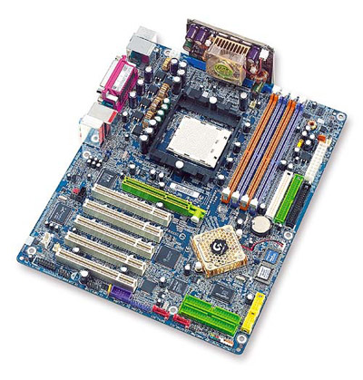
The clear blue board with rounded corners is instantly recognizable as trademark Gigabyte. As you can see, the single-chip nForce3-150 gives designers a little more room for a better board design.
Unlike Athlon XP motherboards, we see a standardized ATX plus 12V connector arrangement on the Athlon64 and FX51 boards we have seen. This is identical to the power connector requirements of current Pentium 4 systems. We generally prefer the connectors together on the upper right of the board, but Gigabyte's placement of the 20-pin ATX to the upper right and the 12V at the top left of the processor socket is acceptable and should allow for decent cable placement.
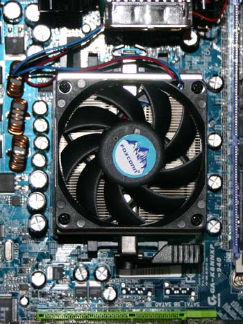
There is plenty of room around the north-to-south sides of the CPU socket, even with the new and much larger Athlon64/64FX heatsink “cage”. Gigabyte has placed the CPU socket away from the top edge to make room for the DPS-K8 power module.
The location of the DPS board on the top edge of the motherboard can be a potential problem in some case designs. It works well in full-tower cases, but many case designs have a downward facing fan to cool the CPU and will be blocked by the DPS-K8 module. With the careful attention to placement of components on the K8NNXP-940, we assume that Gigabyte must have a good reason for choosing this location. You could probably also argue that this location assures the power board stays cool.
The Floppy connector and Primary/Secondary IDE connectors are all in ideal positions. They are in our preferred position above the midline of the board and to the right of the memory slots. This position on the top right edge of the board works well with cable arrangements in almost any case.
The memory slots are arranged so they do not interfere with the AGP card in any way. Changing or adding memory is easy with this arrangement. Gigabyte also uses their EZ-fix AGP lock, which is one of the better designs for securing the AGP card.
Gigabyte K8NNXP-940: BIOS and Overclocking
When we first looked at the Gigabyte pre-release BIOS, we were frankly disappointed. The board did not yield much better performance than the Athlon64 boards we had tested and it was missing the multiplier-unlocking feature. What a difference when we received the shipping F1 BIOS, which managed dramatic leaps in performance and the best Multiplier or Ratio settings that we have seen on an Athlon64 FX board. Considering that this is the first “release” version of the Gigabyte BIOS, we are looking forward to what additional performance Gigabyte may be able to coax from this board in future BIOS revisions.
The K8NNXP-940 uses the familiar Award BIOS, though it will take us all a while to get used to the new options available on HyperTransport boards. Gigabyte also leaves memory timings off their basic BIOS screen, as they have on other recently-released boards.
The Advanced Chipset Features are there — hidden — and you have to enter BIOS with DEL, then hit CTRL+F1 to bring up the hidden menu. We understand why Gigabyte might choose to do this on mainstream boards, but no one would ever accuse the expensive FX51, which requires expensive Registered memory, of being a mainstream choice. Users who will buy the K8NNXP-940 are enthusiasts, and they hardly need to be protected from themselves with a hidden memory timings menu. Gigabyte really needs to rethink this annoying feature, because all it does is create confusion.
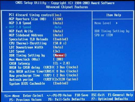
Once you have found the Advanced Chipset Features, you will see a complete selection of memory-tweaking options. The LDT option allows changing Hypertransport speed, and we suggest you leave it alone. When we set LDT to 4.0 (800/1600), it promptly locked the system on reboot. Memory can be left at Auto, which reads the SPD and sets timings, or you can force a memory speed of 100, 133, 150, 166, or 200 representing DDR200 to DDR400.
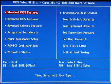
Advanced BIOS Features is a collection of the more common BIOS controls. After initial setup, you will likely see this menu only if you have multiple boot devices, and need to make changes to Boot Order.
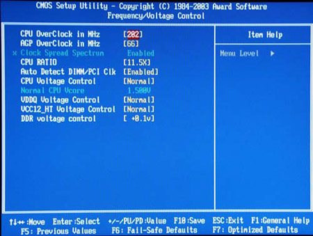
The Frequency/Voltage Control section is where CPU FSB (actually HT speed), CPU multipliers and voltages are set. You can also set AGP/PCI speed in 1MHz increments from 66 to 100. The available voltage options and ranges are what we expect, but have rarely found, on FX boards. We only wish Gigabyte had provided a wider range of DIMM voltage options. Considering FX51 only supports Registered or better memory, the range to +.3V may turn out to be perfectly acceptable. It is too early to determine at this point.
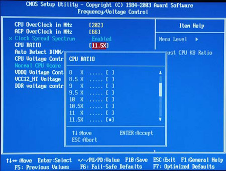
The F1 Release BIOS adds a full range of multipliers to the BIOS options. AMD users have been accustomed to being able to squeeze performance from their chips by changing ratios on the latest Athlon XP/Barton chips. Since Athlon64 did away with unlocked processors, AMD is wise to bring them back to the Athlon64 FX51 "Enthusiast" processor. It adds a bit more value to one of the most expensive CPUs on the market.
vCore or CPU voltage can be set to an unusual range of 0.8V to 1.70V. This may seem to be a strange range, but current 1.45V to 1.5V chips are likely the highest voltage that we will see in production chips, so the range is designed for the future. With Socket 940 due to be replaced with a Socket 939 that does support regular unbuffered memory, we wonder what this really represents in future-proofing. As some have pointed out, Socket 940 will continue for quite a while after FX as an Opteron standard.
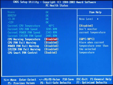
PC Health Status gives a complete display of voltages, temperatures and fan speeds. Feelings are mixed, though, on the “OK” output in the voltage section. Computer Enthusiasts, the target market for this board, would really prefer to see real voltage readouts.
Overall, the BIOS options for the Gigabyte K8NNXP-940 are what we hoped we would see in FX motherboards. Until now, we weren't so sure that we would find this range of tweaking options on the new Athlon64 FX boards. Gigabyte and nVidia have delivered a board with the kinds of control that most Enthusiasts want. Some areas could be improved, but most will find the BIOS options for K8NNXP-940 to be a good selection to squeeze the best performance from their FX processor.
FSB Overclocking Results
With the very complete selection of overclocking options on the Gigabyte, we had very high expectations for the overclocking performance of the board. What we didn't know, and still don't know, however, is what kind of total overclocking range will be available to FX users.| Front Side Bus Overclocking Testbed | ||
| Default Voltage | Maximum Overclock | |
| Processor: | Athlon64 FX51 2.2GHz |
Athlon64 FX51 2.2Ghz |
| CPU Voltage: | 1.5V (default) | 1.6V |
| Cooling: | AMD Stock Athlon64 FX51 Heatsink/Fan | AMD Stock Athlon64 FX51 Heatsink/Fan |
| Power Supply: | Enermax 465W | Enermax 465W |
| Maximum OC: | 2409MHz (+10%) 219FSB |
? |
The above overclocking setup at DEFAULT voltage allowed us to reach a stable FSB of 219MHz. Running our standard Quake3 bench at 2.4GHz yielded Q3 test scores right at 500fps. The maximum overclock, unfortunately, remains a mystery. As you will see in the benchmark suite, the standard test performance with the new F1 BIOS is outstanding. However, there are still problems with multipliers and FSB settings on this motherboard. 11.5X worked until we hit 215FSB; then, mysteriously reset itself to 210, no matter what we set. The 12.0X multiplier worked at 200, and would start generating mysterious FSB and multiplier values above this setting. We even tried downclocking the multiplier, but could not set higher FSB settings that would be retained. We suspect Gigabyte will quickly fix this because this is a very promising board, but for now the Maximum overclock simply cannot be reported. We will revisit this in the near future when we receive a BIOS update.
For a quick comparison, we ran the FX51 in our nVidia Reference board. In that board, by setting the memory to 333, we were able to boot our FX at a CPU setting of 230 at 1.6V. We suspect it may do even better, but with multiplier and FSB settings not completely working, it would be unrealistic to report a maximum overclock at this time. We still believe that with this Gigabyte board, it will be possible to reach the maximum overclock our FX51 chip can achieve. The Gigabyte is remarkably stable in all we can do with it so far, and hopefully a BIOS update will fix the overclocking issues that have surfaced.
Gigabyte K8NNXP-940: Stress Testing
We performed stress tests on the Gigabyte K8NNXP-940 in these areas and configurations:1. Chipset and motherboard stress testing, conducted by running the FSB at 219MHz.
2. Memory stress testing, conducted by running RAM at 400MHz with 2 DIMM slots filled and at 400MHz with all 4 DIMM slots filled at the lowest memory timings possible.
Front Side Bus Stress Test Results:
As is normal in our testing, we ran a full range of stress tests and benchmarks to ensure the Gigabyte K8NNXP-940 was absolutely stable at each overclocked FSB speed. This included Prime95 torture tests, and the addition of other tasks - data compression, various DX8 and DX9 games, and apps like Word and Excel — while Prime95 was running in the background. Finally, we ran our benchmark suite, which includes ZD Winstone suite, Unreal Tournament 2003, SPECviewperf 7.0, and Gun Metal Benchmark 2. At default voltage, 219MHz was the highest overclock that we were able to achieve with the K8NNXP without encountering any reliability issues. We will take another look at the K8NNXP-940 when a new BIOS update corrects the multiplier and FSB adjustment issues.Memory Stress Test Results:
This memory stress test is very basic, as it simply tests the ability of the KX18D PROII to operate at its officially supported memory frequency (400MHz DDR) at the lowest supported memory timings that our Mushkin High Performance ECC Registered Modules will support:| Stable DDR400 Timings — 2 DIMMs (1/2 Dual-Channel banks populated) |
|
| Clock Speed: | 200MHz |
| Timing Mode: | N/A |
| CAS Latency: | 2.0 |
| Bank Interleave: | N/A |
| RAS to CAS Delay: | 3T |
| RAS Precharge: | 8T |
| Precharge Delay: | 2T |
| Command Rate: | N/A |
We currently have 4 DIMMs each of Registered ECC DDR400 from both Legacy Electronics and Mushkin. The Legacy runs well at 2.5-3-4-5 timings, while the Mushkin has SPD timings of 2-2-3-8. Until we complete our upcoming roundup of Registered (ECC) DDR400 memory, we are using the Mushkin as our test standard. We had no problem at all with absolutely stable performance of the Mushkin High Performance ECC Registered at SPD timings.
Filling all available memory banks is more strenuous on the memory subsystem than testing 1 bank (2 DIMMs) in dual-channel mode, as it tests four DIMMs (2 banks) of Registered ECC memory running 400MHz DDR at the most aggressive memory timings the memory will allow.
| Stable DDR400 Timings — 4 DIMMs (2/2 Dual-Channel banks populated) |
|
| Clock Speed: | 200MHz |
| Timing Mode: | N/A |
| CAS Latency: | 2.0 |
| Bank Interleave: | N/A |
| RAS to CAS Delay: | 3T |
| RAS Precharge: | 8T |
| Precharge Delay: | 2T |
| Command Rate: | N/A |
Running both Dual-Channel Banks required the same timings as a single Dual-Channel Bank. It appears you can load the Gigabyte K8NNXP-940 with four DIMMs and still expect the fastest performance that your memory is capable of achieving.
We tested all these memory timings using several stress tests and general applications to guarantee stability. Prime95 torture tests were successfully run at the timings listed in the above charts. We also ran Sciencemark (memory tests only) and Super Pi. None of the three stress tests created any stability problems for the Gigabyte K8NNXP-940 at these memory timings.
Gigabyte K8NNXP: Tech Support and RMA
For your reference, we will repost our support evaluation procedure here:The way our Tech Support evaluation works is first we anonymously email the manufacturer's tech support address(es), obviously not using our AnandTech mail server to avoid any sort of preferential treatment. Our emails (we can and will send more than one just to make sure we are not getting the staff on an “off” day) all contain fixable problems that we have had with our motherboard. We then give the manufacturer up to 72 business hours to respond and then we will report whether or not they responded within the time allotted, and if they were successful in fixing our problems. In case we don't receive a response before the review is published, any future responses will be added to the review, including the total time it took for the manufacturer to respond to our requests.
The idea here is to encourage manufacturers to improve their technical support as well as provide new criteria upon which to base your motherboard purchasing decisions. As motherboards become more similar every day, we have to help separate the boys from the men in as many ways as possible. As usual, we are interested in your feedback on this and other parts of our reviews, so please do email us with your comments.
Gigabyte's RMA policy is easy to follow and fairly good for a tier one motherboard maker. They offer a one-to-three year (depending on the model) manufacturer's Limited warranty. If you are experiencing difficulties in warranty service through your dealer, Gigabyte may attempt to resolve this issue. You must provide the following details to process your RMA request: Name, Address, Phone/Fax number, Model/Revision number, Serial number (10 digits), the precise issues that you are experiencing, name of vendor from which you purchased your Gigabyte product (include vendor contact info), CPU type and size, and memory module type and size. Like ASUS, Gigabyte prefers that you deal directly with the vendor from where you purchased the motherboard rather than directly with them.
In recent tests, Gigabyte has become the first Tier 1 manufacturer to consistently meet our 72-hour reply deadline — which is a vast improvement over past Gigabyte tech support. Since we were testing a pre-release board, any answer we would get from Gigabyte would hardly be a fair measurement of typical consumer response. We therefore decided to delay another Gigabyte tech support test until we were examining a released motherboard. Gigabyte tells us that the K8NNXP-940 should be available at dealers within the next couple of weeks.
Performance Test Configuration
| Performance Test Configuration | |
| Processor(s): | AMD Athlon64 FX51 (2.2GHz) AMD Athlon64 3200+ (2.0GHz) AMD Opteron Socket 940 at 2.0GHz (9x222) 444FSB AMD Athlon XP 3200+ (2.2GHz, 400MHz FSB) Intel Pentium 4 at 3.2GHz (800FSB) Intel Pentium 4 at 3.0GHz (800FSB) |
| RAM: | 2 x 512MB Mushkin Registered ECC DDR400 High Performance 2 x 512MB Mushkin PC3500 Level II 4 x 512MB Legacy ECC at 2.5-3-4-5 2 x 256MB Corsair PC3200 TwinX LL (v1.1 ) |
| Hard Drive(s): | Maxtor 120GB 7200 RPM (8MB Buffer) Western Digital 120GB 7200 RPM (8MB Buffer) |
| Video AGP & IDE Bus Master Drivers: | NVIDIA nForce version 2.45 (7/29/2003) VIA 4in1 Hyperion 4.49 (August 20, 2003) NVIDIA nForce version 2.03 (1/30/03) |
| Video Card(s): | ATI Radeon 9800 PRO 128MB (AGP 8X) |
| Video Drivers: | ATI Catalyst 3.7 |
| Operating System(s): | Windows XP Professional SP1 |
| Motherboards: | Gigabyte K8NNXP-940 (nForce3) Athlon64 FX51 ChaintechZNF3-150 (nForce3) Athlon64 3200+ FIC K8-800T (VIA K8T800) Athlon64 3200+ MSI K8T Neo (VIA K8T800) Athlon64 3200+ nVidia Reference nForce3 Opteron144 @ 222.0 MHz FSB (2.0GHz) DFI NFII Ultra (nForce2 U400) Barton 3200+ Albatron KX18D PROII (nForce2 U400) Barton 3200+ Asus P4C800-E (Intel 875P) 3.2Ghz P4 |
The Athlon64 FX requires Registered or Registered ECC memory. Tests with the Gigabyte K8NNXP-940 were performed with Mushkin High Performance Registered ECC DDR400 memory. Recent performance tests on nForce2 Ultra 400 and Intel 875/865 boards used 2 x 512MB Mushkin PC3500 Level II Double-bank memory. Previous tests of motherboards used 2 x 256MB Corsair 3200LL Ver. 1.1. Mushkin PC3500 L2 was used to preserve the 2-2-2-6 timings that were used in tests with Corsair 3200LL Ver. 1.1. Both Mushkin and Corsair use the same Winbond BH5 memory chips in these modules.
All performance tests were run with the ATI 9800 PRO 128MB video card with AGP Aperture set to 128MB with Fast Write enabled. Resolution in all benchmarks is 1024x768x32.
For the fairest comparisons, benchmarks were recompiled on the Asus P4C800-E using the 3.2GHz Pentium 4 processor.
Additions to Performance Tests
Science Mark 2 Memory Performance, 9/23/03 update, was included to compare Memory Bandwidth and Latency of the Athlon64 FX51 and Pentium 4 3.2GHz. AnandTech has standardized on ZD Labs Multimedia Content Creation Winstone 2003 and ZD Labs Business Winstone 2002 for system benchmarking.Game Benchmarks
We have added Gun Metal DirectX Benchmark 2 from Yeti Labs, the new X2 Benchmark, which includes Transform and Lighting effects, and Aquamark3 to our standard game benchmarks. We will be adding other benchmarks in the near future. Jedi Knight II has been dropped from our standard Benchmark Suite. We were forced to use different patches for operation on Athlon and Intel Pentium 4, which made cross-platform comparison difficult, if not impossible. In addition, Opteron/Athlon64 requires a third patching variation for benchmarking. JK2 uses a Quake engine, and we are continuing Quake3 as a standard benchmark for the time being.Content Creation, General Usage and Memory Performance
Content Creation is a benchmark that has long been dominated by Intel's Pentium 4 processors. It was quite a surprise to see that the Athlon64 FX51 finally hold its own in the test, tying the 3.2 P4 for first place. Athlons have always done well in the Business Winstone bench, and the FX51 just extends the lead.
Science Mark 2 was recently updated, and we used the latest 9/23/03 build for our Memory testing. The real advantage of the on-CPU Memory Controller can clearly be seen in the increased memory bandwidth of the Dual-Channel 2.2GHz FX51 compared to the 3.2GHz Dual-Channel P4. Even more striking is the improvements in latency with the on-CPU controller. The Socket 939 should exhibit even lower memory latencies, since Registered memory does add some latency overhead to these memory scores.
Media Encoding and Gaming Performance
Testing of the Gigabyte K8NNXP-940 shows the FX51 extends the dominance of the Athlon64 in gaming benchmarks that we saw in our first Athlon64 motherboard roundup and the Opteron tested in our Athlon64 preview. The astounding scores in GunMetal 2 by the Dual-Channel Opteron and Athlon64 FX51 are difficult to explain, since they are not duplicated by our single-channel Athlon64 benchmark. We were convinced that these scores on the original Opteron must be a fluke until they showed up again in our tests and retest of the K8NNXP-940 Dual-Channel.
The Athlon64 and Athlon64 FX dominate gaming benchmarks compared to other current processors.
High End Workstation Performance — SPECviewperf 7.0
SPECviewperf has been a standard in the AnandTech test suite for many months. Recently, any test of AMD-based motherboards brought comments about the poor workstation performance compared to Pentium 4. As you can clearly see, those days are over. Even more so than our early tests of Athlon64 and Opteron, the FX51 is competitive to superior in Workstation performance. You can clearly see that this is an area where the added bandwidth of the FX51/Opteron has a real Performance impact.
Final Words
The Gigabyte K8NNXP-940 is an impressive motherboard. The performance it exhibits at standard settings in our benchmarks is simply outstanding. The early impressions of the Athlon64 FX51 were that it was not much faster than Athlon64. Perhaps we should recast this to say that the early Athlon64 FX motherboards were not much faster than the Athlon64 motherboards running Athlon64 processors. In almost every benchmark, the Gigabyte K8NNXP-940 with an Athlon64 FX51 tops our fastest Pentium 4 motherboard — the Asus P4C800-E running a 3.2GHz processor. Even the usual P4 stronghold of Content Creation sees the Athlon64 FX51 and 3.2GHz P4 in a dead heat. In almost every other benchmark, the Athlon64 FX51 is a clear winner — over both the Pentium 4 3.2GHz and the Athlon64 3200+. The only exception here is our Media Encoding benchmark, which tends to favor Intel processors and will soon be replaced with an updated benchmark.The features, layout, and included accessories make the Gigabyte K8NNXP-940 a stellar home for a new FX CPU. Gigabyte has done an outstanding job in the engineering of this Socket 940 motherboard, and in standard testing, it is in every way a winning combination with the Athlon64 FX51. The addition of Multipliers to the release K8NNXP motherboard just sweetens the picture that much more. With the high cost of the FX51, Enthusiasts will need some persuading to pay the price for the FX processor. AMD and Asus were smart to make it clear that the FX51 could be unlocked in the BIOS, unlike regular, cheaper, single-channel Athlon64 chips. Gigabyte becomes the second manufacturer to add the ability to manipulate FX ratios in the BIOS.
With this high praise, we do believe Gigabyte has more work to do on the BIOS of the K8NNXP-940. It is certainly fast and full of options in the release F1 version, but it is disappointing to find that the new CPU ratios do not work reliably, and the FSB often exhibits some strange behaviors — resetting itself to lower values on boot — and we don't just mean default 200. We had two cases where settings of 220 came back at boot as 209.5, and the 12 multiplier only worked at 200 FSB setting.
Despite the issues with the immature BIOS, we still highly recommend the Gigabyte K8NNXP-940. It can take the Enthusiast to new performance heights as it is, and we fully expect even better overclocking with some of the BIOS kinks worked out. It performs better than any Socket 940 board that we have tested so far.
We have been told that we will see at least a couple of new and revised Athlon64 FX motherboards in the near future. They may prove to be even better, in particular, an update with the VIA chipset that is said to have new features for that chipset. However, until we test those Socket 940 boards and perhaps find one that performs even better, the Gigabyte K8NNXP-940 is King of the Hill.


