Original Link: https://www.anandtech.com/show/1119
Gigabyte 7NNXP (nForce2 Ultra 400): Gigabyte Goes nForce
by Evan Lieb on July 5, 2003 10:53 PM EST- Posted in
- Motherboards
In terms of features and speed, Gigabyte’s first foray into NVIDIA chipset-based motherboards is no slouch by any stretch of the imagination. The Gigabyte 7NNXP is based on NVIDIA's latest and greatest Athlon XP chipset, dubbed the nForce2 Ultra 400. The nForce2 Ultra 400 is different from NVIDIA's earlier nForce2 chipsets in only one way; official 400MHz FSB support. Results from NVIDIA's in-house testing confirmed that nForce2 Ultra 400 was able to reach higher FSB speeds than their older chipsets from last year, which reached average speeds of only 420MHz FSB. (However, nForce2 chipset steppings predating nForce2 Ultra 400 did gradually perform a bit better.)
If you refer back to our nForce2 6-way Motherboard roundup in December 2002, you'll see that nForce2 motherboards from ABIT, ASUS, Chaintech, Epox, Leadtek, and MSI were all revision 1.x. In other words, they were not based on the nForce2 Ultra 400 chipset. Now, virtually every single nForce2 motherboard available for purchase is based on NVIDIA’s nForce2 Ultra 400 chipset, and each motherboard is accordingly marked version 2.0. For example, the old ASUS A7N8X Deluxe motherboard (based on the original nForce2 chipset) was a revision 1.x motherboard, while the new ASUS A7N8X Deluxe motherboard (based on the nForce2 Ultra 400 chipset) is a revision 2.0 motherboard. This applies to all other motherboard manufacturers, not just ASUS.
When we first saw the Gigabyte 7NNXP motherboard we were delighted to see so many onboard features that previous nForce2 motherboards lacked. Read on to learn about these new features and why this motherboard may just be part of your next Athlon XP system.
Gigabyte 7NNXP: Basic Features
| Motherboard Specifications | |
| CPU Interface | Socket-462 |
| Chipset | nForce2 Ultra 400 North Bridge nForce2 MCP-T South Bridge |
| Bus Speeds | up to 300MHz (in 1MHz increments) |
| Core Voltages Supported | up to 1.850V (in 0.0250V increments) |
| I/O Voltages Supported | N/A |
| DRAM Voltages Supported | up to 2.80V (in 0.1V increments) |
| Memory Slots | 4 184-pin DDR DIMM Slots |
| Expansion Slots | 1 AGP 8X Slot 5 PCI Slots |
| Onboard IDE RAID | ITE GigaRAID 8212F controller (RAID 0, RAID 1 & RAID 0 + 1) |
| Onboard USB 2.0/IEEE-1394 | Six USB 2.0 ports supported by MCP-T Realtek RTL8801 IEEE-1394 FireWire (up to 3 ports available) |
| Onboard LAN | Dual LAN: Intel PRO/1000 MT Gigabit LAN nForce MCP-T Ethernet |
| Onboard Audio | Realtek ALC650 AC’97 codec (nForce2 APU) |
| Onboard Serial ATA | Two SATA connectors via Silicon Image SI3112A controller (RAID 0, 1 & 0 + 1) |
| BIOS Revision | F9 BIOS (5/30/2003) |
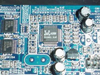
Gigabyte makes a smart move by including NVIDIA’s feature rich and powerful MCP-T South Bridge, which, among other things, contains the nForce2 APU (Audio Processing Unit). We discussed the nForce2 architecture in great detail (NVIDIA nForce2 Preview) in the past. To refresh your memory, the APU is defined by three parameters. The first is support for hardware acceleration of 256 2D voices and 64 3D voices, as well as 3D positional audio. The second is full support of Microsoft’s DX8.0 standard. The third and final parameter (by which the APU is defined) is support for Dolby Digital 5.1 and in-hardware Dolby Digital encoding. The great weakness here is that you can’t take advantage of Dolby Digital Encoding unless you’re using SPDIF (which requires proper speakers with a receiver). Thus, you’ll be forced to use the Analog Out port, which does not bypass the mediocre fidelity of the Realtek ALC650 AC’97 codec. In other words, if you plan on taking advantage of the nForce2 APU’s capabilities, you will need the correct speakers and SPDIF ports.
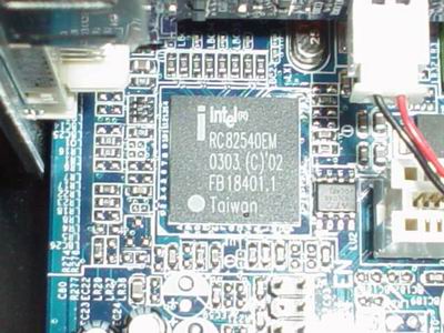
Gigabyte utilizes Intel’s PRO/1000 MT adapter via the 82540EM controller for Gigabit Ethernet. This is what Intel calls their “Desktop” version of the PRO/1000 MT. It is capable of 10/100/1000 Mbps speeds. This is a top notch solution, yet still falls behind Intel’s PRO/1000CT Gigabit solution, which is widely available on the latest 865PE and 875P motherboards and runs through Intel’s new Gigabit bus (CSA), with a dedicated bandwidth of 266MB/s instead of sharing the 133 MB/s PCI bus with other devices.
One feature that is certainly unique in any high-end desktop motherboard is Gigabyte’s patented DPS technology. DPS is a separate, add-in card that gives this motherboard 6-phase power circuitry instead of 3-phase. Gigabyte claims that, in Parallel mode (versus Backup mode), DPS is able to deliver better system stability (especially while overclocked) in addition to longer life of onboard components. While there's no way for us to prove Gigabyte's claim to longer components life without literally testing this motherboards for months/years on end, we can tell you that our FSB overclocking tests did not yield any improvement with DPS installed.
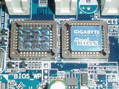
The 7NNXP also includes support for Gigabyte’s much-talked-about dual BIOS technology. Having a backup BIOS is beneficial when you accidentally corrupt your first BIOS chip (i.e. you lose power to your system as you're updating your primary BIOS). Simply switch over to the second BIOS chip, and your machine becomes operational. This feature voids the frustration and inconvenience of correcting the problem through other, time-consuming methods, such as a board RMA or the swap-trick.
The I/O ports configuration of the 7NNXP is fairly standard, aside from the dual Ethernet ports. Included in this setup are two PS/2 ports, two serial ports, one parallel port, four USB 2.0 ports, two LAN ports (one 10/100 and one 10/100/1000), and Mic In, Line In, and Line Out ports, which drive the onboard sound. The IEEE 1394 FireWire support via the Realtek RTL8801 controller can only be found through onboard headers and not through the rear panel, which is a loss in our book. Another unfortunate oversight is the lack of rear SPDIF ports, which would have been exceedingly useful for users who want to take advantage of the nForce2 APU. This would have been more convenient than the bundled SPDIF bracket. Overall this is an acceptable I/O configuration, but it could have been a bit better, especially considering the high-priced nature of this motherboard.
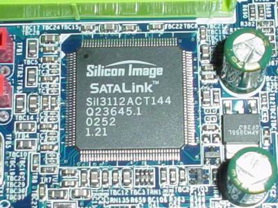
Gigabyte also adds a PCI-bound Serial ATA RAID controller from Silicon Image, dubbed the SI3112A. This controller is used by many motherboard makers, including most of the top tier desktop motherboard makers. This controller supports RAID 0, 1 and 0 + 1 arrays.
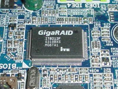
One of the most notable features the 7NNXP carries is onboard IDE RAID from ITE, named the GigaRAID IT8212F controller. There are two onboard IDE connectors that are powered by the GigaRAID IT8212F controller, which is capable of RAID 0 (striping), RAID 1 (mirroring) and RAID 0 + 1 RAID arrays. Not only can this controller support a total of four HDDs (hard disk drives), but four ATAPI (optical) drives as well. This is a considerable advantage over other motherboards with Promise or Silicon Image controllers that are only capable of supporting HDDs.
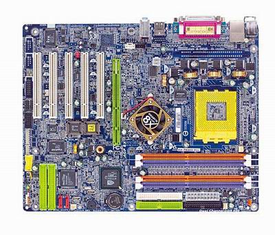
Gigabyte 7NNXP: Board Layout
Overall, we were quite pleased with the 7NNXP’s layout. We like the fact that Gigabyte places the 7NNXP ATX (20-pin) connector at the top right-hand side of the PCB to the right of the DIMM slots. Since standard PSUs do not have an extra long ATX cable, this location is excellent. It will reduce clutter and greatly minimize the intrusive ATX wires from obstructing the installation/uninstallation of the CPU HSF, memory modules, and any other components that you may decide to modify or uninstall in that area. If you’re using a high-quality PSU with an extra-long ATX connector, then you have nothing to worry about, but the ATX connector location is still ideal for those users who can’t afford the best PSUs.
The 7NNXP’s ATX12V connector is located just below the DPS (Dual Power System), one of the 6 “Dual Miracles” that Gigabyte markets with their high-end desktop motherboards. However, it has proven to be nothing more than a marketing gimmick based on our own extensive testing. The location of the ATX12V connector is not ideal since standard PSU’s ATX12V cable runs directly over the CPU HSF. This means that you would have to unhook the ATX12V cable just to uninstall your HSF. As we’ve mentioned countless times before, this is not an issue with higher quality PSUs, but if you’re not overclocking, it seems pointless to spend extra cash on a high-watt, name-brand PSU.
For many reasons, it was wise for Gigabyte to place the Primary and Secondary IDE connectors above the midsection of the motherboard and to the right of the DIMM slots. First, this allows for bundled IDE cables to reach the upper bays of your ATX case. Secondly, it permits installation of optical drives in the first and second bays. This would not be possible if the Primary/Secondary IDE connectors were placed where the IDE RAID connectors are located on the 7NNXP. In addition, this location offers better air flow and case organization, and enables the user to make use of the Slave connector on the bundled IDE cables. All in all, you can’t go wrong with this site.
The position of the Floppy connector is less than ideal, however. In a Floppy drive installation, you’ll notice that the Floppy cable will create some case clutter and disorganization. Fortunately, the Floppy connector is right next to (and slightly above) the Primary/Secondary IDE connectors, and all the connectors will be centrally located. Still, it is not clear why Gigabyte couldn’t just place the Floppy connector at the bottom of the board near the IEEE 1394 FireWire ports.
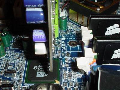
A very nice touch to the 7NNXP is the location of the DIMM connectors. They are far enough away from the AGP slot so that it doesn’t force users to uninstall their video card if they need to install or uninstall some memory. Can you imagine unscrewing your video card, unplugging your VGA cable, and physically uninstalling your video card from the AGP slot just to swap memory? Slowly, but surely, motherboard makers are taking notice of this complaint and are properly implementing the changes during layout decisions. DFI was the first of several motherboard makers to acknowledge openly that their engineers literally designed their motherboard around user requests.
Gigabyte 7NNXP: BIOS and Overclocking
Gigabyte continues to utilize the Award BIOS on 100% of their desktop motherboards with the 7NNXP.
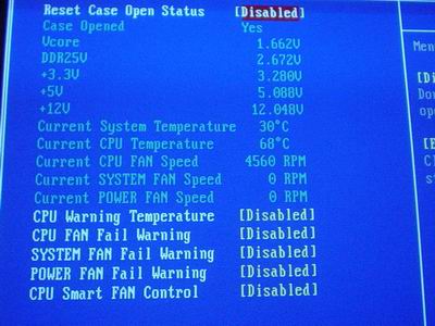
The 7NNXP PC Health section includes such readings as System and CPU temperatures, CPU, System, and Power fan speeds, Vcore, VDIMM, and PSU readings (all rails). Gigabyte adds in other options, such as a “CPU Smart Fan Control” option that regulates the speed of your CPU HSF depending on the task at hand. Unfortunately, this option cannot be adjusted or tweaked in any way; you can only disable or enable CPU Smart Fan Control. Other features that you can use in the PC Health section are CPU/System/Power Fan Fail Warning options, which can be enabled or disabled, and a CPU Warning Temperature option that, when enabled, will shut down your system (90C is the maximum value you can set this option).
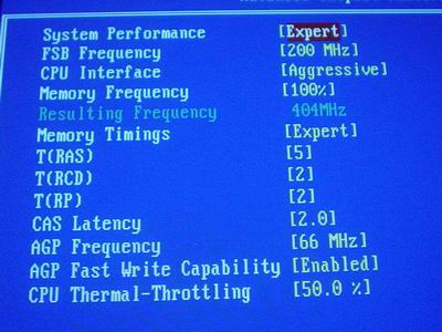
Gigabyte continues the tradition of using the CTRL + F1 method of revealing memory-related tweaking options in the BIOS. However, the 7NNXP BIOS does not hide the Advanced Chipset Features section like in previous Gigabyte motherboards. This time, holding the CTRL key and pressing F1 simply reveals more tweaking options within the Advanced Chipset Features section (make sure to press CTRL + F1 outside of the Advanced Chipset Features section, not inside). Anyway, this section contains the usual collection of memory timing options, such as CAS Latency, RAS to CAS Delay, RAS Precharge, and Precharge Delay. There are also other very important performance-related options, such as FSB frequency, AGP frequency, memory frequency, AGP fast write option and, finally, the CPU interface option (Aggressive or Optimal available). This is a very well organized and structured Advanced Chipset Features section. However, we would prefer it if Gigabyte would leave out the CTRL + F1 setting in future BIOSes, unless of couse Gigabyte’s research has proven that it causes fewer problems with end users who are novices at setting up a BIOS.
As mentioned, there are FSB frequency adjustments available in the Advanced Chipset Features section. The 7NNXP FSB ceiling is 300MHz FSB, which is more than enough for the most adventurous overclockers out there. You will never reach anywhere near this frequency reliably, so don’t worry about maxing out your CPU’s FSB anytime in the future, especially since AMD will not be using anything higher than a 400MHz FSB when the Athlon eventually dies.
Gigabyte offers decent VDIMM control within the 7NNXP BIOS. VDIMM is available up to 2.8V in 0.1V increments. This should be plenty for the vast majority of users out there. However, for those users who aren’t pleased with 2.8V, you may find it comforting to know that the 7NNXP naturally overvolts by 0.07V; thus, 2.87V is the maximum attainable memory voltage the 7NNXP can reach.
The Vcore options available in the 7NNXP BIOS are adequate, though not all that great. Vcore is available as high as 1.850V in 0.0250V increments. The increments in which Vcore can be tuned is more disappointing than the somewhat low Vcore ceiling. We would have preferred 0.0125V adjustments instead, as finer adjustments are never a bad thing and can be easily implemented. Still, 0.0250V should suffice for most users. The 1.850V ceiling should also be more than enough for most overclockers, though there will undoubtedly be adventurous overclockers that will want to push further than 1.850V. In those cases the 7NNXP does not fit the bill.
According to Gigabyte, the AGP and PCI buses are locked at their default frequencies (66MHz/33MHz) regardless of the FSB frequency. The AGP lock is evident from looking at the AGP frequency options in the Advanced Chipset Features section. On the other hand, the PCI lock is hidden and cannot be independently adjusted like the AGP bus. Nevertheless, the 7NNXP still has an AGP/PCI lock and that’s all that matters.
The VAGP adjustments available in the 7NNXP BIOS are just fine. VAGP is adjustable in 0.1V increments up to 1.8V, and should suit just about anyone looking to increase their VAGP.
One final feature that adds a nice touch to the 7NNXP is chipset voltage adjustments. The 7NNXP BIOS allows chipset voltage adjustments of 5%, 7.5%, and 10%. Thankfully the nForce2 Ultra 400 North Bridge onboard the 7NNXP is equipped with an active North Bridge heatsink, otherwise we would have suggested the addition of active cooling.
FSB Overclocking Results
For FSB overclocking, the following setup was used on the Gigabyte 7NNXP:
| Front Side Bus Overclocking Testbed | |
| Processor: | Athlon XP 2500+ (Barton Core) |
| CPU Vcore: | 1.650V (default) |
| Cooling: | Volcano 7+ HSF |
| Power Supply: | Enermax 350W |
The above overclocking setup allowed us to reach a stable FSB of 222MHz. This is not to be unexpected from an nForce2 Ultra 400 motherboard, especially one from a top tier motherboard maker such as Gigabyte. Having examined dozens of KT400, KT400A, and a select few KT600 motherboards, we can confidently say that nForce2 Ultra 400 motherboards are the only choice for overclockers. In general, we were quite pleased with the tweaking and overclocking options the 7NNXP BIOS afforded us, and so running at 222MHz FSB (8X multiplier) was a joy.
The multiplier range of the 7NNXP BIOS allowed us to isolate the FSB to see how hard we could push the 7NNXP without other factors interfering. Fortunately, there are multiplier adjustments available in 0.5 increments from 5.5 to 12.5, and up to 20 in scattered increments.
Gigabyte 7NNXP: Stress Testing
We performed stress tests on the 7NNXP in several different areas and configurations, including:
1. Chipset and motherboard stress testing was conducted by running the FSB at 222MHz
2. Memory stress testing was conducted by running RAM at 400MHz with two DIMM slots filled and at 400MHz with all four DIMM slots filled in dual DDR mode at the lowest timings possible.
Front Side Bus Stress Test Results:
As standard practice, we ran a large load of stress tests and benchmarks to ensure the 7NNXP was absolutely stable at each overclocked FSB speed. These stress tests included Prime95 torture tests, which were run in the background for a total of 24 hours.
We proceeded to run several other tasks, such as data compression, various DX8 games, and light apps like Word and Excel with Prime95 running in the background. Finally, we reran our entire benchmark suite, which includes Sysmark 2002, Quake3 Arena, Unreal Tournament 2003, SPECviewperf 7.0, Jedi Knight 2 and XMPEG. In the end, 222MHz FSB was the highest overclock we were able to achieve with the 7NNXP without encountering any reliability issues.
Memory Stress Test Results:
This memory stress test examines the motherboard’s ability to operate at its officially supported memory frequency (400MHz DDR), and at the lowest supported memory timings that our Corsair TwinX LL modules support:
| Stable Dual DDR400 Timings (2/4 banks populated) |
|
| Clock Speed: | 200MHz |
| Timing Mode: | N/A |
| CAS Latency: | 2.0 |
| Bank Interleave: | N/A |
| RAS to CAS Delay: | 2T |
| RAS Precharge: | 4T |
| Precharge Delay: | 2T |
| Command Rate: | N/A |
It’s not surprising to see that the 7NNXP achieved such low memory timings with just two memory modules spec’ed at DDR400 running in dual channel DDR400 mode. It is standard for any P4 or Athlon XP motherboard to achieve these aggressive performance settings, though only nForce2 and nForce2 Ultra 400 motherboards can achieve a RAS Precharge as low as 4T. However, we suggest you run your memory at CAS 2-2-2-5 instead, as we discovered some time ago that CAS 2-2-2-4 is a bit slower than CAS 2-2-2-5. Of course, the difference will never be noticeable in real world usage.
The following memory stress test is obviously a bit more strenuous on the memory subsystem than most memory stress tests, as it tests for stability when a desktop user installs four DIMMs running in dual DDR400 mode at the most aggressive memory timings attainable in the BIOS:
| Stable Dual DDR400 Timings (4/4 banks populated) |
|
| Clock Speed: | 200MHz |
| Timing Mode: | N/A |
| CAS Latency: | 2.0 |
| Bank Interleave: | N/A |
| RAS to CAS Delay: | 3T |
| RAS Precharge: | 6T |
| Precharge Delay: | 2T |
| Command Rate: | N/A |
It is not unusual to see such lax timings for such a strenuous memory subsystem test such as this. However, we have seen better and so in this case, the 7NNXP does not perform as well as most other modern-day motherboards. Again, the real world performance difference is negligible, so we urge you not to flip out ove small variances in memory timings as seen in the two charts above.
We tested all these memory timings using several stress tests and general applications to guarantee stability. We initiated the tests by running Prime95 torture tests; a grand total of 24 hours of Prime95 was successfully run at the timings listed in the above charts. We also ran Sciencemark (memory tests only) and Super Pi. All three stress tests could not make the 7NNXP fail at the timings listed in the above charts.
Gigabyte 7NNXP: Tech Support and RMA
For your reference, we will repost our support evaluation procedure here:
The way our Tech Support evaluation works is first we anonymously email the manufacturer's tech support address (es), obviously not using our AnandTech mail server to avoid any sort of preferential treatment. Our emails (we can and will send more than one just to make sure we are not getting the staff “on” an "off" day) all contain fixable problems that we have had with our motherboard. We then give the manufacturer up to 72 hours to respond over business days and will report not only whether they even responded within the time allotted but also if they were successful in fixing our problems. After publishing the review, if we do eventually receive a response we will go back and amend the review with the total time it took for the manufacturer to respond to our requests.
The idea here is to encourage manufacturers to improve their technical support as well as provide new criteria to base your motherboard purchasing decisions upon; with motherboards looking more and more alike every day, we have to help separate the boys from the men in as many ways as possible. As usual, we are interested in your feedback on this and other parts of our reviews so please do email us with your comments.
Gigabyte's RMA policy is easy to follow and fairly good for a tier one motherboard maker. They offer a one-to-three year (depending on the model) manufacturer's Limited warranty. If you are experiencing difficulties in warranty service through your dealer, Gigabyte may attempt to resolve this issue. You must provide the following details to process your RMA request: Name, Address, Phone/Fax number, Model/Revision number, Serial number (10 digits), the precise issues you are experiencing, vendor from which you purchased your Gigabyte product from, (include vendor contact info), CPU type and size, and memory module type and size.
Like ASUS, Gigabyte prefers that you deal directly with the vendor from where you purchased the motherboard rather than with them. This is understandable, as the cost of RMAs, facilities, employees, etc. can be prohibitive. Still, we would love it if the tier one manufacturers would adopt similar RMA policies akin to Epox, Albatron or AOpen's policies.
We were pleased to see that Gigabyte's tech support responded within 72 hours; 33 hours to be exact. This is a vast improvement over Gigabyte's past tech support record, and hopefully it will continue. Though Gigabyte's RMA policy is only adequate, in this instance their tech support performance was excellent. We certainly hope this is the start of a trend.
Performance Test Configuration
| Performance Test Configuration | |
| Processor(s): | AMD Athlon XP 3200+ (400MHz FSB) |
| RAM: | 2 x 256MB Corsair PC3200 TwinX LL (v1.1) Modules (SPD rated at CAS 2-2-2-6) |
| Hard Drive(s): | Western Digital 120GB 7200 RPM Special Edition (8MB Buffer) |
| Bus Master Drivers: | NVIDIA nForce version 2.03 (January 30, 2003) VIA 4in1 Hyperion 4.47 (May 20, 2003) |
| Video Card(s): | MSI GeForce4 Ti 4600 (AGP 4X) |
| Video Drivers: | NVIDIA Detonator 44.03 (May 14, 2003) |
| Operation System(s): | Windows XP Professional SP1 |
| Motherboards: | Epox 8KRA2+ (KT600) @ 202.44MHz FSB Gigabyte 7NNXP (nForce2 Ultra 400) @ 202.77MHz FSB |
All performance tests run on nForce2 Ultra 400 motherboards utilized two 256MB Corsair TwinX LL PC3200 (v1.1) modules set to CAS 2-2-2-5 timings in dual channel DDR400 mode. All performance tests run on the KT600-based 8KRA2+ utilized the two Corsair modules listed in the chart above with the following performance settings:
| DDR400 Timings (2/3 banks populated) |
|
| Clock Speed: | 200MHz |
| Timing Mode: | Ultra |
| CAS Latency: | 2.0 |
| Bank Interleave: | 4-bank |
| RAS to CAS Delay: | 2T |
| RAS Precharge: | 6T |
| Precharge Delay: | 2T |
| Command Rate: | 1T |
- AGP fast write enabled
- AGP Aperture set to 128MB
Content Creation & General Usage Performance
Media Encoding and Gaming Performance
High End Workstation Performance - SPEC Viewperf 7.0
High End Workstation Performance (continued...) - SPEC Viewperf 7.0
Final Words
After much testing, we can safely conclude that the Gigabyte 7NNXP is the most feature-filled Athlon XP motherboard we’ve ever tested. The combination of features such as IDE and Serial ATA RAID, dual LAN, dual BIOS, and IEEE 1394 FireWire, among other contributing factors, led us to this conclusion. Certainly, ASUS and ABIT’s nForce2 Ultra 400 motherboards are excellent choices for a high-end Socket A motherboard, and in general, are quite comparable to the 7NNXP's feature set. But in terms of pure onboard features (and BIOS features too), the Gigabyte 7NNXP manages to be a cut above the rest.
The only real negative thing we can say about the 7NNXP is that it doesn’t offer much bang for your buck, as it’s approximately $60 more expensive than its slightly less featured cousin, the 7N400 Pro. The 7N400 Pro is identical to the 7NNXP in every way except for two things; lack of a second onboard LAN controller (the Intel version) and the DPS technology. For $60 less, you’d be crazy to pass up the 7N400 Pro if you don’t require the second LAN port or DPS unit. In fact, if we had to choose between the Gigabyte 7N400 Pro, ABIT NF7-S and ASUS A7N8X Deluxe, we’d choose the 7N400 Pro any day of the week. All three motherboards are priced nearly the same in the U.S., so there’s little point in passing up a motherboard that offers more features and the same performance for the exact same price tag.
Therefore, we have no problem recommending the Gigabyte 7NNXP or 7N400 Pro to Athlon XP users who desire the absolute fastest motherboard with stellar overclocking ability, in addition to the best feature set we've seen from any Athlon XP motherboard to date. Currently, we are examining DFI’s nForce2 Ultra 400 LAN Party motherboard, and it has shown potential thus far. You may want to wait for the verdict on that review, but regardless of the outcome, we can safely say you won’t be making a bad choice by purchasing Gigabyte’s 7N400 Pro or 7NNXP today.


