Original Link: https://www.anandtech.com/show/9886/amd-reveals-polaris-gpu-architecture
AMD Reveals Polaris GPU Architecture: 4th Gen GCN to Arrive In Mid-2016
by Ryan Smith on January 4, 2016 9:00 AM EST
For much of the last month we have been discussing bits and pieces of AMD’s GPU plans for 2016. As part of the Radeon Technology Group’s formation last year, the leader and chief architect of the group, Raja Koduri, has set about to make his mark on AMD’s graphics technology. Along with consolidating all graphics matters under the RTG, Raja and the rest of the RTG have also set about to change how they interact with the public, with developers, and with their customers.
One of those changes – and the impetus for these recent articles – has been that the RTG wants to be more forthcoming about future product developments. Traditionally AMD always held their cards close to their chest about architectures, keeping them secret until the first products based on a new architecture launch (and even then sometimes not talking about matters in detail). With the RTG this is changing, and similar to competitors Intel and NVIDIA, the RTG wants to prepare developers and partners for new architectures sooner. As a result the RTG has been giving us a limited, high-level overview of their GPU plans for 2016.
Back in December we started things off talking about RTG’s plans for display technologies – DisplayPort, HDMI, Freesync, and HDR – and how the company would be laying the necessary groundwork in future architectures to support their goals for higher resolution displays, more ubiquitous Freesync-over-HDMI, and the wider color spaces and higher contrast of HDR. The second of RTG’s presentations that we covered was focused on their software development plans, including Linux driver improvements and the consolidation of all of RTG’s various GPU libraries and SDKs under the GPUOpen banner, which will see these resources released on GitHub as open source projects.
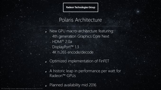
Last but not least among RTG’s presentations is without a doubt the most eagerly anticipated subject: the hardware. As RTG (and AMD before them) has commented on in the past couple of years, a new architecture is being developed for future RTG GPUs. Dubbed Polaris (the North Star), RTG’s new architecture will be at the heart of their 2016 GPUs, and is designed for what can now be called the current-generation FinFET processes. Polaris incorporates a number of new technologies, including a 4th generation Graphics Core Next design for the heart of the GPU, and of course the new display technologies that RTG revealed last month. Finally, the first Polaris GPUs should be available in mid-2016, or roughly 6 months from now.
First Polaris GPU Is Up and Running
But before we dive into Polaris and RTG’s goals for the new architecture, let’s talk about the first Polaris GPUs. With the first products expected to launch in the middle of this year, to no surprise RTG has their first GPUs back from the fab and up & running. To that end – and I am sure many of you are eager to hear about – as part of their presentation RTG showed off the first Polaris GPU in action, however briefly.
As a quick preface here, while RTG demonstrated a Polaris based card in action we the press were not allowed to see the physical card or take pictures of the demonstration. Similarly, while Raja Koduri held up an unsoldered version of the GPU used in the demonstration, again we were not allowed to take any pictures. So while we can talk about what we saw, at this time it’s all we can do. I don’t think it’s unfair to say that RTG has had issues with leaks in the past, and while they wanted to confirm to the press that the GPU was real and the demonstration was real, they don’t want the public (or the competition) seeing the GPU before they’re ready to show it off. That said, I do know that RTG is at CES 2016 planning to recap Polaris as part of AMD’s overall presence, so we may yet see the GPU at CES after the embargo on this information has expired.
In any case, the GPU RTG showed off was a small GPU. And while Raja’s hand is hardly a scientifically accurate basis for size comparisons, if I had to guess I would wager it’s a bit smaller than RTG’s 28nm Cape Verde GPU or NVIDIA’s GK107 GPU, which is to say that it’s likely smaller than 120mm2. This is clearly meant to be RTG’s low-end GPU, and given the evolving state of FinFET yields, I wouldn’t be surprised if this was the very first GPU design they got back from Global Foundries as its size makes it comparable to current high-end FinFET-based SoCs. In that case, it could very well also be that it will be the first GPU we see in mid-2016, though that’s just supposition on my part.
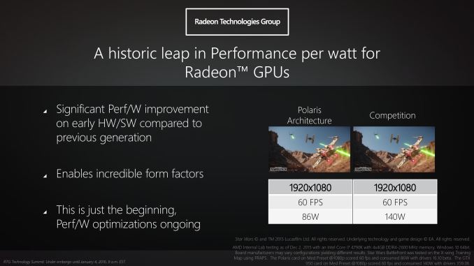
For their brief demonstration, RTG set up a pair of otherwise identical Core i7 systems running Star Wars Battlefront. The first system contained an early engineering sample Polaris card, while the other system had a GeForce GTX 950 installed (specific model unknown). Both systems were running at 1080p Medium settings – about right for a GTX 950 on the X-Wing map RTG used – and generally hitting the 60fps V-sync limit.
The purpose of this demonstration for RTG was threefold: to showcase that a Polaris GPU was up and running, that the small Polaris GPU in question could offer performance comparable to GTX 950, and finally to show off the energy efficiency advantage of the small Polaris GPU over current 28nm GPUs. To that end RTG also plugged each system into a power meter to measure the total system power at the wall. In the live press demonstration we saw the Polaris system average 88.1W while the GTX 950 system averaged 150W. Meanwhile in RTG’s own official lab tests (and used in the slide above) they measured 86W and 140W respectively.
Keeping in mind that this is wall power – PSU efficiency and the power consumption of other components is in play as well – the message RTG is trying to send is clear: that Polaris should be a very power efficient GPU family thanks to the combination of architecture and FinFET manufacturing. That RTG is measuring a 54W difference at the wall is definitely a bit surprising as GTX 950 averages under 100W to begin with, so even after accounting for PSU efficiency this implies that power consumption of the Polaris video card is about half that of the GTX 950. But as this is clearly a carefully arranged demo with a framerate cap and a chip still in early development, I wouldn’t read too much into it at this time.
Polaris: What’s In a Name?
One area where AMD/RTG struggled quite a bit with their existing Graphics Core Next GPUs has been on giving the press and the public consistent and meaningful architecture names. The matter of product naming has always encompassed a certain degree of strife, as a single product can have multiple names: an architecture name, a retail name, a development name, etc. Coupled with the fact that not all of these names are meant to be used in the public, and a certain need to avoid calling attention to architectural differences in what consumers are supposed to perceive as a homogenous product line, and it can quickly become a confusing mess.
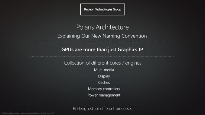
Thankfully for Polaris, RTG is revising their naming policies in order to present a clearer technical message about the architecture. Beginning with Polaris, RTG will be using Polaris as something of an umbrella architecture name – what RTG calls a macro-architecture – meant to encompass several aspects of the GPU. The end result is that the Polaris architecture name isn’t all that far removed from what would traditionally be the development family codenames (e.g. Evergreen, Southern Islands, etc), but with any luck we should be seeing more consistent messaging from RTG and we can avoid needing to create unofficial version numbers to try to communicate the architecture.
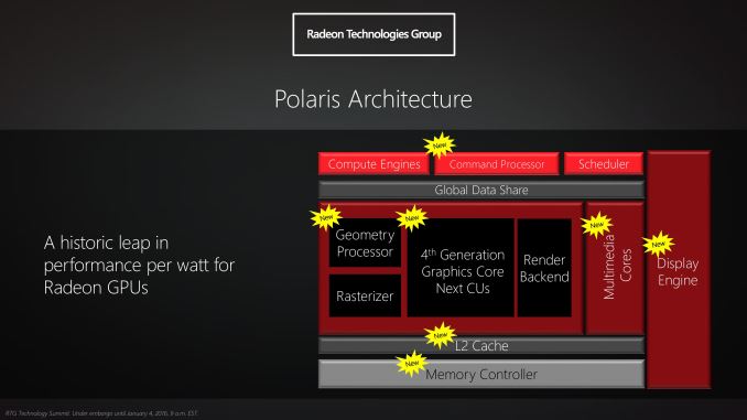
To that end the Polaris architecture will encompass a few things: the fourth generation Graphics Core Next core architecture, RTG's updated display and video encode/blocks, and the next generation of RTG's memory and power controllers. Each of these blocks is considered a seperate IP by RTG, and as a result they can and do mix and match various versions of these blocks across different GPUs, such as the GCN 1.2 based Fiji containing an HEVC decoder but not the GCN 1.2 based Tonga. This, consequently, is part of the reason why AMD has always been slightly uneasy about our unofficial naming. What remains to be seen then is how (if at all) RTG goes about communicating any changes should they update any of these blocks on future parts, and whether say a smaller update like a new video decoder would warrant a new architecture name.
As for the Polaris name itself, RTG tells us that Polaris was chosen as a nod to photons, and ultimately energy efficiency. Though it’s not clear right now what the individual GPUs will be named (if they get names at all), but given the number of stars in the universe RTG certainly isn’t at risk of running out of codenames in the near future.
The Polaris Architecture: At A High Level
As I briefly mentioned a bit earlier in this article, today’s reveal from RTG is not meant to be a deep dive into Polaris, fourth generation GCN, or any other aspect of RTG’s architecture. Rather today is meant to offer a very high level overview of RTG’s architectural and development plans – similar to what we traditionally get from Intel and NVIDIA – with more information to come at a later date. So it’s fair to say that today’s reveal won’t answer many of the major questions regarding the architecture, but it gives us the briefest of hints of what we’ll be talking about in depth here later this year.
The Polaris architecture encompasses several different RTG technologies, and with a focus on energy efficiency RTG claims that this will be largest jump in performance per watt in the history of Radeon GPUs. At its heart is RTG’s fourth generation Graphics Core Next architecture, which despite the generational naming is easily the biggest change to RTG’s shader core architecture since the launch of first generation of GCN GPUs in 2012. Officially RTG has not assigned a short-form name to this architecture at this time, but as reading the 8-syllable “fourth generation GCN” name will get silly rather quickly, for now I’m going to call it GCN 4.
For GCN 4, RTG will be making a number of changes in order to improve the efficiency of the architecture from both a throughput perspective and a power perspective. Of the few details revealed to us, one of the things we have been reassured of is that GCN 4 is still very much Graphics Core Next. I expect that means retaining the current 16-wide vector SIMD as the base element of the architecture, in which case it should be fair to say that while GCN 4 is the biggest change to GCN since its introduction, RTG is further building on top of GCN rather than throwing large parts out.
RTG’s few comments, though obviously made at a very high level, offer a good deal of insight on where we should expect GCN 4 to go from a throughput perspective. Overall RTG packs quite a bit of hardware into their GCN GPUs, with Fiji reaching 4096 FP32 stream processors, however putting all of those SPs to good use has been difficult for RTG. This is something we’ve seen first-hand over the last year, as the Radeon Fury ended up being surprisingly close to the Fury X in performance despite the difference in SP counts. Similarly, the recent launch of DirectX 12 and the first uses of asynchronous shading have shown that RTG’s architectures at times significantly benefit from the technology, which is an indicator that they haven't always been able to fill up their SPs with work under normal circumstances.
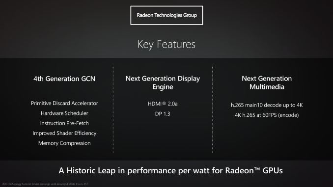
As a result a lot of the disclosed GCN 4 key features point to improving throughput of GCN. Improved shader efficiency is somewhat self-explanatory in that regard. At the same time RTG is also disclosing that we will be seeing some kind of hardware scheduler in GCN 4 along with instruction pre-fetch capabilities, which again should help them improve throughput in ways to be determined. Meanwhile in an improvement for the GPU front-end, GCN 4 will be adding a primitive discard accelerator – and again we don’t have any further details than this – but it should help the architecture clamp down on getting rid of unseen geometry. Finally, GCN 4 will also include a newer generation of RTG’s memory compression technology, this coming just one generation after it was most recently (and significantly) improved for the third generation GCN architecture (GCN 1.2).
What isn’t mentioned in RTG’s key features for GCN 4 but is clearly a major aspect of the core architecture’s design is energy efficiency. While RTG will be drawing a significant amount of their energy efficiency gains from the switch to FinFET (more on this in a bit), the architecture will also play a large role here. RTG was upfront in telling us that on average the node shrink will probably count for more of Polaris's gains than architecture improvements, but this will also be very workload dependent. In order to make that happen the architecture team has been spending quite a bit of time on the matter, analyzing and simulating different workloads and architecture options to find ways to improve the architecture. Truthfully I’m not really sure how much of this will ever be disclosed by RTG – energy efficiency is very much the secret sauce of the GPU industry these days – but hopefully we’ll get to find out more about what kind of energy optimizations GCN 4 includes closer to the launch of the first GPUs.
Meanwhile along with the improvements coming courtesy of GCN 4, Polaris also encompasses RTG’s updated display and multimedia capabilities. As we covered the display tech last month I won’t dwell on that too much here, but suffice it to say Polaris includes a new display controller that will support the latest DisplayPort and HDMI standards.
Finally, along with today’s announcement RTG is also disclosing a bit of what we can expect for Polaris’s multimedia controllers. On the decode side RTG has confirmed that Polaris will include an even more capable video decoder than Fiji; along with existing format support for 8-bit HEVC Main profile content, Polaris’s decoder will support 10-bit HEVC Main10 profile content. This goes hand-in-hand with the earlier visual technologies announcement, as 10-bit encoding will be necessary to prevent banding and other artifacts with the wider color spaces being used for HDR. Meanwhile RTG’s UVD video encode block has also been updated, and HEVC encoding at up to 4K@60fps will now be supported, marking a major jump over the previous generation encoder block only supporting H.264. There is no word on whether that will include Main10 support as well, however.
Polaris Hardware: GDDR5 & HBM
Although not a part of RTG’s presentation, along with the architecture itself we also learned a few items of note about RTG’s hardware plans that I wanted to mention here.
First and foremost, Polaris will encompass both GDDR5 and High Bandwidth Memory (HBM) products. Where the line will be drawn has not been disclosed, but keeping in mind that HBM is still a newer technology, it’s reasonable to expect that we’ll only see HBM on higher-end parts. Meanwhile the rest of the Polaris lineup will continue to use GDDR5, something that is not surprising given the lesser bandwidth needs of lower-end parts and the greater cost sensitivity.
Meanwhile RTG has also disclosed that the first Polaris parts are GDDR5 based. Going hand-in-hand with what I mentioned earlier about RTG’s Polaris demonstration, it seems likely that this means we’ll see the lower-end Polaris parts first, with high-end parts to follow.
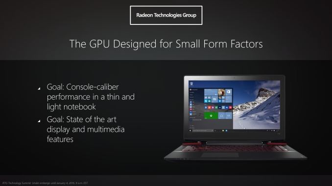
As for the specific laptop and desktop markets, RTG tells us that desktop and mobile Polaris parts will launch close together. I wouldn’t be surprised if mobile is RTG’s primary focus since it’s already the majority of PC sales, but even so desktop users shouldn’t be far behind.
Polaris: Made For FinFET
The final aspect of RTG’s Polaris hardware presentation (and the bulk of their slide deck) is focused on the current generation FinFET manufacturing processes and what that means for Polaris.
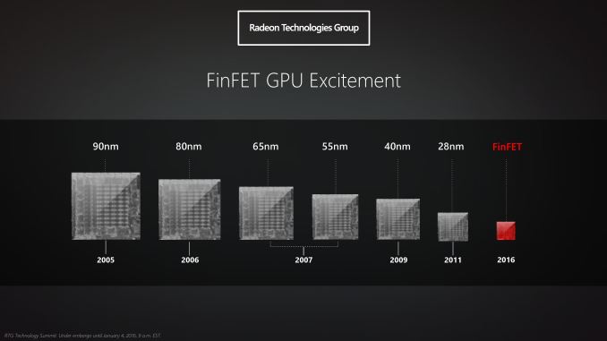
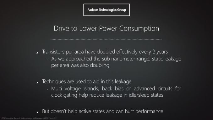
As RTG’s slide concisely and correctly notes, the regular march of progress in semiconductor fabrication has quickly tapered off over the last decade. What was once a yearly cadence of new manufacturing processes – a major new node every 2 years with a smaller step in the intermediate years – became just every two years. And even then, after the 20nm planar process proved unsuitable for GPUs due to leakage, we are now to our fifth year of 28nm planar as the leading manufacturing node for GPUs. The failure of 20nm has essentially stalled GPU manufacturing improvements, and in RTG’s case resulted in GPUs being canceled and features delayed to accommodate the unexpected stall at 28nm.
For their most recent generation of products both RTG and NVIDIA took steps to improve their architectural efficiency due to the lack of a new manufacturing process – with NVIDIA having more success at this than RTG – but ultimately both parties were held back from what they originally were planning back around 2010. So to say that the forthcoming move to FinFET for new GPUs is a welcome change is an understatement; after nearly half a decade of 28nm GPUs we finally will see the kind of true generational improvements that can only come from a new manufacturing node.
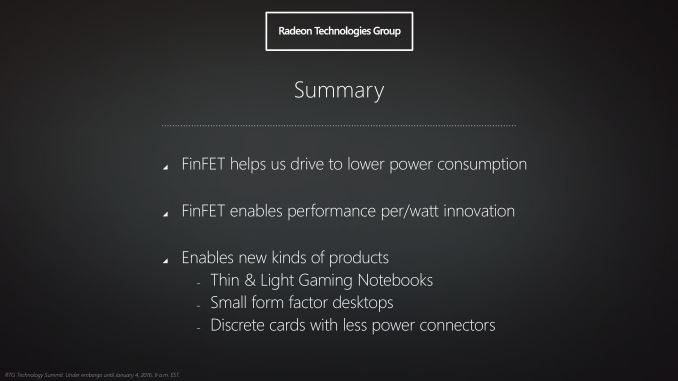
To no surprise then, RTG is aggressively targeting FinFET with Polaris and promoting the benefits thereof. With power efficiency essentially being the limiting factor to GPU performance these days, the greatest gains can only be reached by improving overall power efficiency, and for RTG FinFETs will be a big part of getting there. Polaris will be the first RTG architecture designed for FinFETs, and coupled with the architecture improvements discussed earlier, it should result in the largest overall increase in performance per watt for any Radeon GPU family.
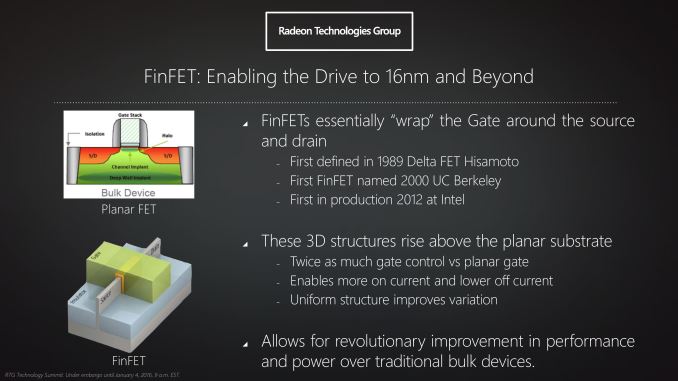
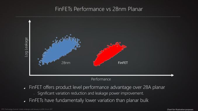
We’ve already covered the technical aspects of FinFET a number of times before, so I’m not going to go into too much depth here. But at the most basic level, FinFETs are the solution to the leakage problems that have made planar transistors impractical below 28nm (and ultimately killed 20nm for GPUs). By using multiple fins to essentially make a transistor 3D, it becomes possible to control leakage in a manner not possible with planar transistors, and that in turn will significantly improve energy efficiency by reducing the amount of energy a GPU wastes just to be turned on.
With the introduction of FinFET manufacturing processes, GPU manufacturing can essentially get back on track after the issues at 20nm. FinFETs will be used for generations to come, and while the initial efficiency gain from adding FinFETs will likely be the single greatest gain, it solves the previous leakage problem and gives foundries a route to 10nm and beyond. At the same time however as far as the Polaris GPUs are concerned, it should be noted that the current generation of 16nm/14nm FinFET processes are not too far removed from 20nm with FinFETs. Which is to say that the move to FinFETs gets GPU manufacturing back on track, but it won’t make up for lost time. 14nm/16nm FinFET is essentially only one generation beyond 28nm by historical performance standards, and the gains we're expecting from the move to FinFET should be framed accordingly.
As for RTG’s FinFET manufacturing plans, the fact that RTG only mentions “FinFET” and not a specific FinFET process (e.g. TSMC 16nm) is intentional. The group has confirmed that they will be utilizing both traditional partner TSMC’s 16nm process and AMD fab spin-off (and Samsung licensee) GlobalFoundries’ 14nm process, making this the first time that AMD’s graphics group has used more than a single fab. To be clear here there’s no expectation that RTG will be dual-sourcing – having both fabs produce the same GPU – but rather the implication is that designs will be split between the two fabs. To that end we know that the small Polaris GPU that RTG previewed will be produced by GlobalFoundries on their 14nm process, meanwhile it remains to be seen how the rest of RTG’s Polaris GPUs will be split between the fabs.
Unfortunately what’s not clear at this time is why RTG is splitting designs like this. Even without dual sourcing any specific GPU, RTG will still incur some extra costs to develop common logic blocks for both fabs. Meanwhile it's also not clear right now whether any single process/fab is better or worse for GPUs, and what die sizes are viable, so until RTG discloses more information about the split order, it's open to speculation what the technical reasons may be. However it should be noted that on the financial side of matters, as AMD continues to execute a wafer share agreement with GlobalFoundries, it’s likely that this split helps AMD to fulfill their wafer obligations by giving GlobalFoundries more of AMD's chip orders.
Closing Thoughts
And with that, we wrap up our initial look at RTG's Polaris architecture and our final article in this series on RTG's 2016 GPU plans. As a high level overview what we've seen so far really only scratches the surface of RTG's plans - and this is very much by design. But as the first occasion of RTG opening up their roadmaps and giving us a bit of a look into the future, it's a welcome change not only for developers, but for the press and public alike.
Backed by the first major node shrink for GPUs in over 4 years, RTG has laid out an aggressive plan for Polaris in 2016. At this point RTG needs to catch up and close the market share gap with NVIDIA - of this RTG is quite aware - and Polaris will be the means to do that. What needs to happen now is for RTG to fully execute on the plans they've laid out, and if they can do so then 2016 should turn out to be an interesting (and competitive) year in the GPU industry.

