Original Link: https://www.anandtech.com/show/9233/amds-2016-gpu-roadmap-finfet-high-bandwidth-memory
AMD’s 2016 GPU Roadmap: FinFET & High Bandwidth Memory
by Ryan Smith on May 6, 2015 2:01 PM EST- Posted in
- AMD
- Radeon
- GPUs
- AMD FAD 2015

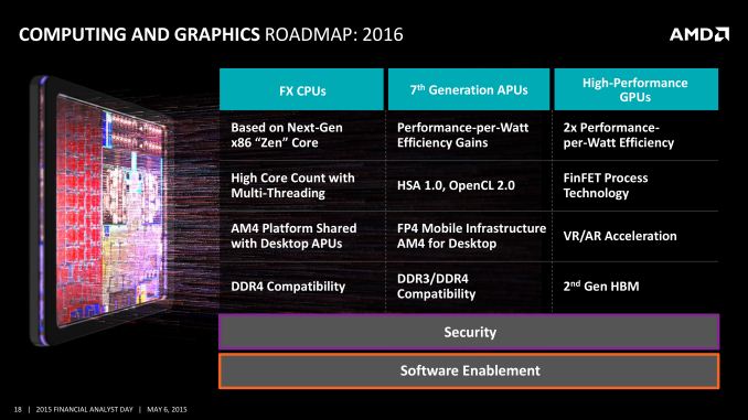
Along with updating their x86 and CPU roadmaps, AMD has also offered a brief update on their GPU roadmap. Unfortunately unlike 2012 we’re not going to get anything quite like the HSA feature roadmap, which projected features out for the next few years, but AMD is opening up on what is in store for 2016.
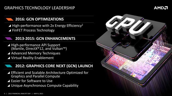
First and foremost, 2016 will be the year of FinFET across AMD, both for the CPU and GPU. Just like Zen, AMD will have GPUs on an unnamed FinFET process in 2016. AMD isn’t saying much else about 2016 at this point in terms of chips or architecture, but they are saying that the combination of the 2016 architecture and the use of FinFET will result in a 2x improvement in energy efficiency over what AMD is calling their “previous generation GPU” (though it’s not clear if it’s relative to an existing GPU or something else due in 2015). Based on AMD’s comments, it sounds like the majority of these gains will come from the use of the newer manufacturing process, as opposed to architectural efficiency gains. AMD is also mum on which fab will be building this GPU, however the timeframe is such that it lines up with TSMC’s 16nm FinFET plans, with TSMC being AMD’s traditional fab of choice for GPUs.
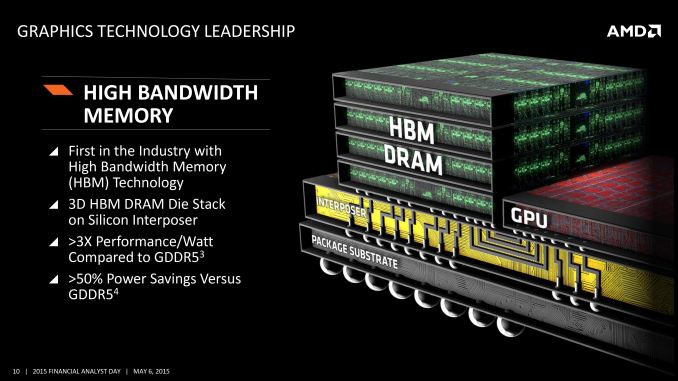
Meanwhile after the circulation of a number of rumors, AMD has confirmed that they will be shipping GPUs with High Bandwidth Memory (HBM) technology. HBM involves stacking DRAM dies on top of each other, and then locating them next to or on top of a processor, the close proximity allowing for a very wide, very high bandwidth memory bus. AMD isn’t saying what absolute performance is like at this time, but HBM should better than triple their memory perf-per-watt compared to GDDR5, with a better than 50% reduction in power consumption.
AMD’s roadmap and diagrams also make it clear that we’re looking at a 2.5D solution; that is, HBM RAM stacks organized around a processor rather than on top of it. These stacks are then routed to the processor based on an interposer layer that both the RAM stacks and processor sit in, and the interposer itself sits above the traditional package substrate. Given the high thermal output of high-end GPUs, this is what we’d expect as putting RAM on top of the GPU would make it that much harder to cool.
Finally, AMD is stating that they expect to be the first vendor to deploy HBM, meaning that we’re looking at a launch of an HBM-equipped video card sooner than NVIDIA’s Pascal, which was previously announced to be using the same technology.


