Original Link: https://www.anandtech.com/show/923
Computex 2002 Day 2: ATI's R300, nForce2 & XScale PDAs
by Anand Lal Shimpi on June 4, 2002 11:24 AM EST- Posted in
- Trade Shows
While the first day of Computex was stolen by AMD's Hammer announcements today's events were spread out much more evenly among a handful of companies. Through the sweltering heat while drowning in humidity in Taipei we managed to grab photos of ATI's R300, NVIDIA's nForce2 and learn even more about the omnipresent Hammer platform from AMD.
We provided an exclusive look at Intel's Springdale chipset to our Newsletter Subscribers earlier today and now we're offering the same information from that piece in our Day 2 wrap up coverage as well. If you'd like to receive these exclusive looks first you'll want to sign up for our free Newsletter here.
VIA Demonstrates ATI's R300
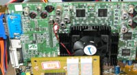
While in VIA's suite we noticed a couple of demos running, one of which happened to be a test of AGP 8X functionality on the KT400 chipset. Although VIA's AGP 8X controller still has issues with SiS' Xabre 400 core, VIA wanted to prove that the chipset did in fact support AGP 8X so they displayed it running with the only other AGP 8X graphics card they had access to - ATI's R300.
Just a few weeks ago we were in Toronto visiting ATI and they were very tight lipped about anything R300 related; it will be interesting to see if VIA was supposed to be publicly running this R300 in their suite.
There wasn't much we could gather from seeing the R300 run demo loops over and over again; benchmarking it was out of the question. The card was stable and as you can probably guess by now, this was the card that was running Doom 3 at E3 a couple weeks ago. The reason id Software was demonstrating Doom 3 on the R300 is simply because ATI has the fastest GPU that is in a stable enough form to actually run for any appreciable period of time. ATI's release schedule has always given them the ability to beat NVIDIA to the punch when it comes down to their Fall product releases. ATI usually releases in the Summer and NVIDIA follows in the Fall. The development of R300 has placed it in a very healthy state today and we are expecting to hear an announcement from ATI in the July/August timeframe.
Given that the chip is already up and running and production is due soon we are beginning to wonder if the R300 will be made on a 0.13-micron process or if it will be 0.15-micron like its predecessor. If it is indeed a 0.15-micron chip then there is the question of whether ATI will make it a DX9 compliant part with full floating point pipelines. Assuming ATI does make the R300 as feature rich as NVIDIA's NV30 currently appears on paper, then there's the question of yield and clock speeds. It will be interesting to see the design choices ATI made with the R300 and how that effects competition with the NV30 later this year.
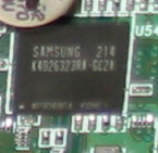 The
one thing that we could gather from the card that VIA was running is an idea
of memory clock speeds. The DDR SDRAM chips used on the 128MB R300 card were
2.86ns parts rated at 350MHz, thus you can assume an effective memory clock
of 700MHz. It is also safe to assume that the R300 has a 256-bit memory bus
much like the Parhelia-512 and 3DLabs P10 GPUs resulting in 22.4GB/s of raw
memory bandwidth without taking any sort of occlusion culling technology into
consideration. Granted that this isn't an indication of final shipping clock
speeds but it should give you a ballpark figure to expect from R300. With ATI
providing boards for E3 and VIA's AGP 8X test, it will only be a matter of time
before we see cards in reviewers' hands and eventually on store shelves.
Oh and KT400
Seeing the R300 made us forget about exactly what we were looking at - the only KT400 system at Computex that was running with DDR400 memory. The KT400 platform VIA was demonstrating was supposedly running at DDR400 without any issues which is more than any of VIA's motherboard manufacturers have been able to say; it is worth mentioning that it's almost always the case that the chipset manufacturer has no problems with running their own chipset but it's motherboard manufacturers that run into the vast majority of the problems. We're still hearing talk of an August launch for KT400 yet motherboard manufacturers aren't necessarily excited about the upcoming chipset.
We had a chance to talk to VIA about their Pentium 4 strategy which, as we've outlined in our P4X333 Review, is truly limited by the legal matters surrounding their ability to manufacture and sell Pentium 4 chipsets. Coming down the road for Pentium 4 chipsets are the P4X400 which will add DDR400 support to the Pentium 4, as well as the P4X600 which will offer dual channel DDR support for the P4 as well. Because of availability issues VIA is considering bundling DDR400 memory with their P4X400 boards when they do end up shipping later this year.
K8HTA up and running
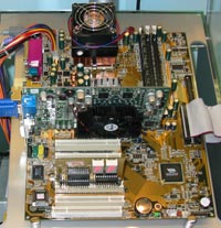
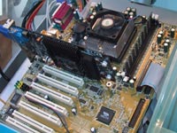
VIA also had their K8HTA Hammer chipset up and running in their suite. The 800MHz/1MB L2 ClawHammer was definitely not running as hot as the processor will once it's clocked closer to its shipping clock speeds but it was apparently running reliably.
VIA's K8HTA reference board was seen in virtually every single motherboard manufacturer's booth or suite but this was the only one that was actually up and running.
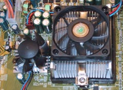
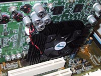
The AGP controller had an interesting heatsink/fan combo (right) and was running quite hot.
Intel's Springdale Chipset
This first appeared on the AnandTech Newsletter. Click Here to Subscribe.
After a number of relatively unsuccessful chipset releases, Intel is finally getting their act together and returning to the glory days of being at the top of the chipset business. The Pentium 4 and Xeon chipsets that Intel has released over the past several months have been impressive but they can't even begin to compete with what Intel has coming right around the corner.
Yesterday we talked about Intel's Granite Bay chipset, a dual-channel DDR solution for the high-end desktop and workstation markets but today we learned much about Intel's Springdale chipset.
The Springdale chipset will be sampling in Q4 of this year and should be expected in mass production quantities sometime in the first half of next year. The chipset will feature an updated graphics core (supposedly faster than 845G which is definitely necessary) as well as a dramatically improved I/O Controller Hub (ICH aka South Bridge).
The Springdale Graphics & Memory Controller Hub (GMCH) does have some significant improvements over the current 845G MCH. Other than the improved graphics core (Intel will probably offer a version without integrated graphics), the chipset will offer support for dual channel DDR333 SDRAM bringing a total of 5.3GB/s of memory bandwidth to the CPU.
The chipset will support the current 533MHz FSB Northwood processors as well as the forthcoming Prescott CPU which is currently planned to offer a 667MHz FSB. Intel is also internally referring to the processor-MCH interconnect as a Processor Side Bus (PSB) instead of a Front Side Bus (FSB), just in case you run into that terminology here or elsewhere; the two are identical. We'll talk more about Prescott in a bit, but for now it's important to note that the dual channel DDR333 memory controller will offer exactly enough bandwidth for Prescott's 667MHz FSB (5.3GB/s).
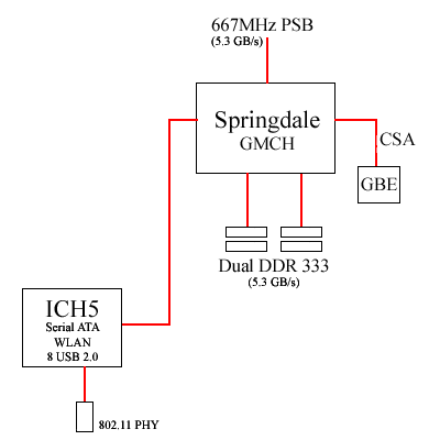
The Springdale GMCH features a new interface that Intel is currently calling their Communications Streaming Architecture (CSA). The CSA bus is an interconnect between the (G)MCH and a high-speed LAN device (e.g. Gigabit Ethernet). The point of the dedicated bus is apparently to prevent Gigabit Ethernet from saturating the MCH/ICH link in the chipset or the PCI bus. The current diagrams of Springdale indicate only one CSA port on the GMCH with aggregate bandwidth equal to about 2Gbps. It will be interesting to get more information on CSA once Intel officially starts talking about it but until then we'll have to live with the rough idea we currently have of it.
The big feature of Springdale is the new Intel ICH5 chip it uses. Serial ATA support and 8 USB 2.0 ports are some of the basic features of the new ICH. Intel will also be releasing a new version of their Application Accelerator (IAA) software that enables software RAID on the new ICH around the release of Springdale. The biggest feature of ICH5 is its integrated Wireless LAN controller (currently 802.11b but that could change by the time it ships); the beauty of the integrated wireless MAC is that a motherboard manufacturer only has to offer an external physical layer (PHY) and wireless LAN can be had relatively cheaply. This is akin to what happened with on-board audio where Intel introduced an AC'97 controller into their ICHs and motherboard manufacturers simply used a cheap AC'97 link on the motherboard itself to offer affordable on-board audio.
There may be a couple versions of Springdale (e.g. Springdale, Springdale-E, Springdale-G) but the basic idea of the platform is as we've just illustrated. The platform will be made available before the release of Prescott but it's clear that the chipset is truly intended to be paired up with the next-generation Pentium 4 processor from Intel.
An Update on Prescott
This first appeared on the AnandTech Newsletter. Click Here to Subscribe.
We first got confirmation of Prescott from Intel at IDF earlier this year and today we received a bit of an update.
It seems as if Intel is playing through all of the possible scenarios that could occur in the CPU industry over the next several months and may be pulling Prescott's launch in a bit. We're now hearing that Prescott may be launched as early as Q2 of next year or as late as Q3 which does fall in their original 2H-2003 estimates. Motherboard manufacturers are preparing themselves for a launch around mid-2003.
Currently Prescott is said to have a 667MHz FSB which is down from the 800MHz FSB Intel originally had expected. If you take into account that Intel is effectively abandoning RDRAM on the desktop side of things and that DDR333 won't be able to offer the 6.4GB/s of memory bandwidth necessary for a 800MHz FSB then it makes sense to introduce Prescott with a 667MHz FSB. This doesn't mean that the chip won't eventually scale to a 800MHz FSB if/when DDR400 or DDR-II take off, but at its launch you can expect it to be a 667MHz solution. Intel may introduce both 533MHz and 667MHz FSB versions of the Prescott core but it's unclear at this point.
There's little information available about the architectural improvements Intel will be making to the core but we are continually hearing that the 0.09-micron core will be outfitted with a large 1MB L2 cache. Hyper Threading will be enabled obviously and the minimum clock speed for Prescott will be 3GHz. Considering that Intel is on track to be at 3GHz by the end of this year on the 0.13-micron Northwood core, we'd say that 3GHz is a very conservative estimate for the 0.09-micron Prescott.
Working ClawHammer Samples at Computex
This first appeared on the AnandTech Newsletter. Click Here to Subscribe.
Although there are a number of mechanical samples of the 754-pin ClawHammer CPU, there are a few working engineering samples at Computex. We were able to get a bit of information about these CPUs. The samples are indeed running at 800MHz but interestingly enough they have a 1MB L2 cache. We're not expecting the desktop ClawHammer CPUs to have a 1MB L2 cache but are very curious in AMD's reasoning behind providing samples with such a large L2 cache.
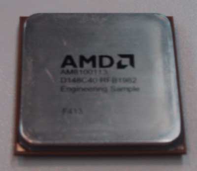
The low clock speed is worrying some motherboard manufacturers but there is still a lot of confidence that AMD will hit their ~2GHz clock speed estimate by the end of the year. If AMD were able to hit it today they would obviously be touting the success so the real question is what clock speed they are currently able to hit. As a first attempt at 0.13-micron SOI as well as an extremely complicated 754-pin package it would be beyond amazing if AMD could hit 2GHz today.
nForce2 - Not Repeating the Same Mistakes
Last year's Computex was almost entirely NVIDIA-centric with the announcement of their nForce chipset that was supposed to revolutionize the chipset industry; fast-forward to the present day and it's clear that it hasn't. One of the problems with the nForce launch was that the chipset was "launched" so much earlier than the actual date when you could buy motherboards based on it; the chipset was announced at Computex and we didn't see boards until the very end of last year and no real design wins until just recently.
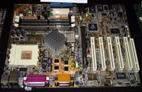
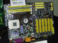
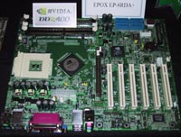
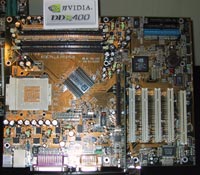
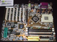
nForce2 Motherboards
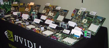
While a number of the architectural improvements that went into nForce's successor (nForce2) improve on weaknesses with the original product, NVIDIA's marketing strategy also reflects this approach. The chipset won't officially be launched until later this summer and although NVIDIA is letting manufacturers show off board designs they are not allowing us to release detailed information on the chipset itself. Here is what we can share with you:
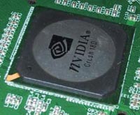
- There is obviously a new Integrated Graphics Processor (IGP) - Crush 18. There will be two derivatives of the Crush 18 IGP, a version with integrated graphics and one without. The integrated graphics core is NV17 derived (with a core clock around the 250MHz clock of the GeForce4 MX 420) and the rest of the IGP will be relatively similar to the previous IGP with a few improvements.
- DDR333 and DDR400 are both supported by the new IGP.
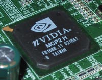
- MCP2 is the new MCP for nForce2 and will be made available in a couple of versions. The APU and basic features of the original MCP remain unchanged.
NVIDIA had a number of nForce2 boards on display in their suite which you can see below; the boards should be available in an August-October timeframe.
NVIDIA's Take on Hammer w/ Integrated Graphics
With our first day of Computex coverage we pointed out that NVIDIA's CK8 solution did not make use of an on-board frame buffer for the integrated graphics. We asked NVIDIA about this today and their response was that an on-board frame buffer completely kills the reasoning behind an integrated graphics solution which is to reduce cost. NVIDIA only commented that they had their best core logic engineers (many of which were hired from Intel according to NVIDIA) working with AMD on the best way to hide memory access latencies with the on-die Hammer memory controller.
NVIDIA did add that they don't see the Hammer nForce solution being a serious volume product until the second half of next year and thus they weren't too concerned with the performance of the integrated graphics this early in the game.
2 SATA + 1 ATA133
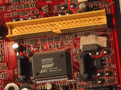
Yesterday we pointed out an interesting combination of three ATA-133 channels on Gigabyte's Hammer motherboard and wondered why the odd number of connectors on the board; today we were able to find out.
Serial ATA Channels to the
left and right of the Promise chip & 1 ATA-133 Connector
Until Intel's Springdale chipset is launched, the only way of getting Serial ATA support on a motherboard is through an external controller. One of the controllers that seems to be quite popular among motherboard manufacturers today is the Promise PDC20376. This particular controller offers two Serial ATA ports as well as a single ATA-133 channel which is why a number of motherboards at Computex feature three ATA-133 channels. The controller also allows for RAID setups using one or more of the channels (Serial ATA or ATA-133) driven by the Promise chip.
V-Link or HyperTransport?
While visiting DFI we noticed that they had a Hammer board design with an AMD AGP 8X controller but with an ALi South Bridge. When we asked them why they chose the odd combination we realized something we hadn't thought of before - motherboard manufacturers won't be able to use VIA South Bridges with AMD AGP controllers for Hammer. The reason being that AMD's chipset uses HyperTransport to connect all of the chips while VIA uses their own V-Link architecture which isn't compatible with HyperTransport.
ALi however does use HyperTransport (as does NVIDIA) and thus there may be some incentive for motherboard manufacturers to look elsewhere outside of VIA for Hammer South Bridge solutions.
ASUS' XScale PDAs
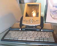
Over at the ASUS booth we saw quite an interesting piece of hardware. As you may know, ASUS has been hitting the mobile market hard with their ASUS line laptops and mobile solutions. Computex 2002 brings the arrival of a new ASUS mobile device: the MyPal A600.
The MyPal A600 is a XScale based PDA solution and happens to be the first one we have seen. Based on the 400MHz PXA250 XScale CPU, the MyPal A600 is certainly large step forward for PocketPCs. The product boasts impressive specs, including: a 3.5 inch, 240x320 pixel, 65,536 color, 3.3 inch TFT LCD; an internal SD/MMC slot; 64MB RAM; 32MB flash ROM, and; up to 12 hours of battery life.
The features are certainly there, but what is really special about the ASUS MyPal A600 is its size. At 4.92" x 2.95" x 0.5", the MyPal A600 is significantly smaller than other PocketPC solutions currently on the market. Naturally, a package this small also has a very low weight: the MyPal A600 weighs in at a mere 5.3 ounces. Take a look at the table below and see why we were excited to hear that the MyPal 600 will be available in about a month and will be shipping to the US.
|
ASUS
MyPal A600
|
Palm
m515
|
Compaq
iPaq H3870
|
|
| Height |
4.92
in
|
4.5
in
|
5.3
in
|
| Width |
2.95
in
|
3.1
in
|
3.3
in
|
| Depth |
0.5
in
|
0.5
in
|
0.62
in
|
| Weight |
5.3
oz
|
4.9
oz
|
6.7
oz
|
Final Words
We're gathering our information and pictures for a large article on future motherboards as we do every year after Computex. We'll keep you posted on that as well as other findings from the show floor, stay tuned and be sure to sign up to our Newsletter to get all of the latest information as soon as we receive it.

