Original Link: https://www.anandtech.com/show/6446/nvidia-launches-tesla-k20-k20x-gk110-arrives-at-last
NVIDIA Launches Tesla K20 & K20X: GK110 Arrives At Last
by Ryan Smith on November 12, 2012 9:00 AM ESTContinuing our SC12 related coverage today, while AMD was the first GPU announcement of the day they are not the only one. NVIDIA is also using the venue to launch their major GPU compute product for the year: Tesla K20.
We first saw Tesla K20 at NVIDIA’s 2012 GPU Technology Conference, where NVIDIA first announced the K20 along with the already shipping K10. At the time NVIDIA was still bringing up the GPU behind K20 – GK110 – with the early announcement at GTC offering an early look at the functionality it would offer in order to prime the pump for developers. At the time we knew quite a bit about its functionality, but not its pricing, configuration, or performance.
More recently, upon completion of K20 NVIDIA has dedicated most of the initial allocation to Oak Ridge National Laboratory’s Titan supercomputer, completing delivery on a contract years in the making. As it turned out K20 was quite powerful indeed, and with K20 providing some 90% of the computational throughput of the supercomputer, Titan has taken the #1 spot on the fall Top500 supercomputer list.
This brings us to today. With Titan complete NVIDIA can now focus their attention and their GPU allocations towards making the Tesla K20 family available to the public at large. With SC12 and the announcement of the new Top500 list as their backdrop, today NVIDIA will be officially launching the Tesla K20 family of compute GPUs.
| NVIDIA Tesla Family Specification Comparison | ||||||
| Tesla K20X | Tesla K20 | Tesla M2090 | Tesla M2070Q | |||
| Stream Processors | 2688 | 2496 | 512 | 448 | ||
| Core Clock | 732MHz | 706MHz | 650MHz | 575MHz | ||
| Shader Clock | N/A | N/A | 1300MHz | 1150MHz | ||
| Memory Clock | 5.2GHz GDDR5 | 5.2GHz GDDR5 | 3.7GHz GDDR5 | 3.13GHz GDDR5 | ||
| Memory Bus Width | 384-bit | 320-bit | 384-bit | 384-bit | ||
| VRAM | 6GB | 5GB | 6GB | 6GB | ||
| Single Precision | 3.95 TFLOPS | 3.52 TFLOPS | 1.33 TFLOPS | 1.03 TFLOPS | ||
| Double Precision | 1.31 TFLOPS (1/3) | 1.17 TFLOPS (1/3) | 655 GFLOPS (1/2) | 515 GFLOPS (1/2) | ||
| Transistor Count | 7.1B | 7.1B | 3B | 3B | ||
| TDP | 235W | 225W | 250W | 225W | ||
| Manufacturing Process | TSMC 28nm | TSMC 28nm | TSMC 40nm | TSMC 40nm | ||
| Architecture | Kepler | Kepler | Fermi | Fermi | ||
| Launch Price | >$3199 | $3199? | N/A | N/A | ||
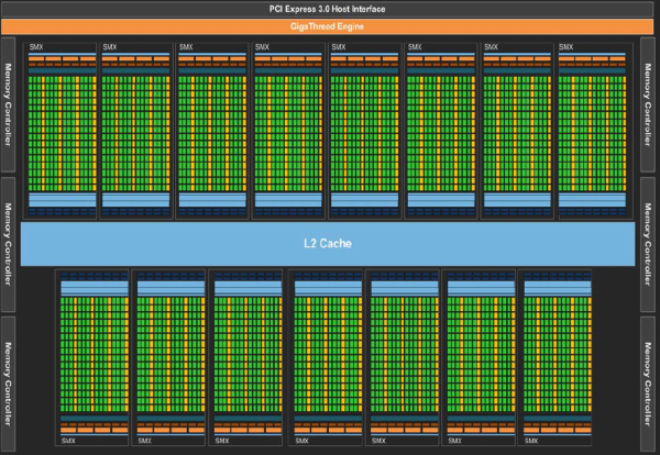
When NVIDIA first announced K20 back in May we were given a number of details about the GK110 GPU that would power it, but because they were still in the process of bringing up the final silicon for GK110 we knew little about the shipping configuration for K20. What we could say for sure is that GK110 was being built with 15 SMXes, 6 memory controllers, 1.5MB of L2 cache, and that it would offer double precision (FP64) performance that was 1/3rd its single precision (FP32 rate). Now with the launch of the K20 we finally have details on what the shipping configurations will be for K20.
First and foremost, K20 will not be a single GPU but rather it will be a family of GPUs. NVIDIA has split up what was previously announced as a single GPU into two GPUs: K20 and K20X. K20X is the more powerful of these GPUs, featuring 14 active SMXes along with all 6 memory controllers and 1.5MB of L2 cache, attached to 6GB of GDDR5. It will be clocked at 732MHz for the core clock and 5.2GHz for the memory clock. This sets a very high bar for theoretical performance, with FP32 performance at 3.95 TFLOPS, FP64 performance at 1.31 TFLOPS, and fed by some 250GB/sec of memory bandwidth. For those of you who have kept an eye on Titan, these are the same specs as the GPUs Titan, and though NVIDIA would not name it at the time we can now confirm that Titan is in fact composed of K20X GPUs and not K20.
Below K20X will be the regular K20. K20 gives up 1 SMX and 1 memory controller, giving it 13 SMXes, 5 memory controllers, 1.25MB of L2 cache, and 5GB of GDDR5. It will also be clocked slightly lower than K20X, with a shipping core clock of 706MHz while the memory clock is held at 5.2GHz. This will give K20 theoretical performance numbers around 3.52 TFLOPS for FP32, 1.17 TFLOPS for FP64, fed by 208GB/sec of memory bandwidth.
This split ends up being very similar to what NVIDIA eventually did with the Fermi generation of Tesla products such as the M2090 and M2075, spacing their products not only by performance and pricing, but also by power consumption. K20X will be NVIDIA’s leading Tesla K20 product, offering the best performance at the highest power consumption (235W). K20 meanwhile will be cheaper, a bit slower, and perhaps most importantly lower power at 225W. On that note, despite the fact that the difference is all of 10W, 225W is a very important cutoff in the HPC space – many servers and chasses are designed around that being their maximum TDP for PCIe cards – so it was important for NVIDIA to offer as fast a card as possible at this TDP, alongside the more powerful but more power hungry K20X. This tiered approach also enables the usual binning tricks, allowing NVIDIA to do something with chips that won’t hit the mark for K20X.
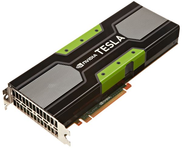
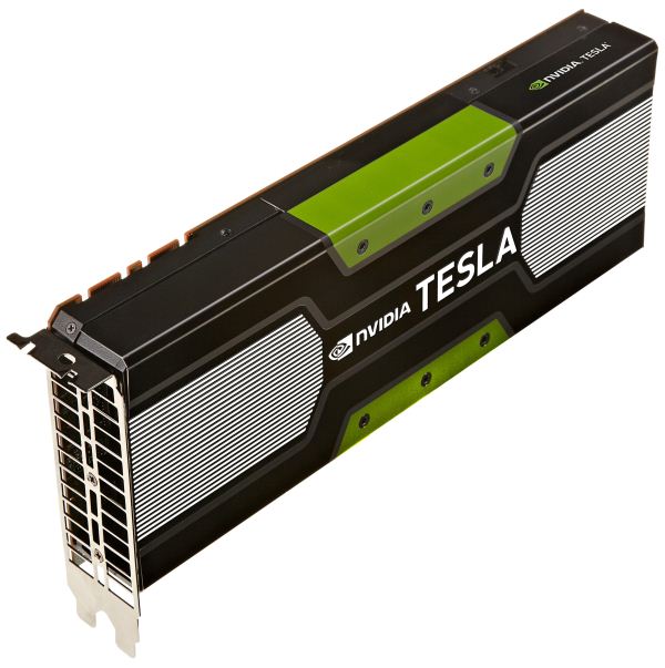
Moving on, at the moment NVIDIA is showing off the passively cooled K20 family design, confirming in the process that both K20 and K20X can be passively cooled as is the standard for servers. NVIDIA’s initial wave of focus for the Telsa K20 is going to be on servers (it is SC12 after all), but with K20 also being an integral part of NVIDIA’s next-generation Maximus strategy we’re sure to see actively cooled workstation models soon enough.
NVIDIA Launches Tesla K20, Cont
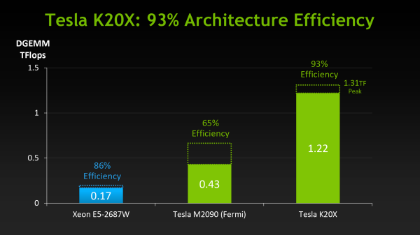
To put the Tesla K20's performance in perspective, this is going to be a very significant increase in the level of compute performance NVIDIA can offer with the Tesla lineup. The Fermi based M2090 offered 655 GFLOPS of performance with FP64 workloads, while the K20X will straight-up double that with 1.31 TFLOPS. Meanwhile in the 225W envelope the 1.17 TFLOPS K20 will be replacing the 515 GFLOPS M2075, more than doubling NVIDIA’s FP64 performance there. As for FP32 workloads the gains are even greater due to the fact that NVIDIA’s FP64 rate has fallen from ½ on GF100/GF110 Fermi to 1/3 on GK110 Kepler; the 1.33 TFLOPS M2090 for example is being replaced by the 3.95 TFLOPS K20X.
Speaking of FP32 performance, when asked about the K10 NVIDIA told us that K20 would not be replacing K10, rather the two will exist side-by-side. K10 actually has better FP32 performance at 4.5 TFLOPs (albeit split across two GPUs), but as it’s based on the GK104 GPU it lacks some Tesla features like on-die (SRAM) ECC protection and HyperQ/Dynamic Parallelism. For the user base that could already be sufficiently served by the K10 it will continue to exist for those users, while for the FP64 users and users who needed ECC and other Tesla features K20 will now step up to the plate as NVIDIA’s other FP32 compute powerhouse.
The Tesla K20 family will be going up against a number of competitors, both traditional and new. On a macro level the K20 family and supercomputers based on it like Titan will go up against more traditional supercomputers like those based on IBM’s BlueGene/Q hardware, which Titan is just now dethroning in the Top500 list.
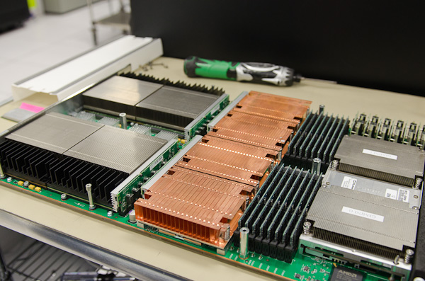
A Titan compute board: 4 AMD Opteron (16-core CPUs) + 4 NVIDIA Tesla K20 GPUs
Meanwhile on a micro/individual level the K20 family will be going up against products like AMD’s FirePro S9000 and FirePro S10000, along with Intel’s Xeon Phi, their first product based on their GPU-like MIC architecture. Both the Xeon Phi and FirePro S series can exceed 1 TFLOPS FP64 performance, making them potentially strong competition for the K20. Ultimately these products aren’t going to be separated by their theoretical performance but rather their real world performance, so while NVIDIA has a significant 30%+ lead in theoretical performance over their most similar competition (FirePro S9000 and Xeon Phi) it's too early to tell whether the real world performance difference will be quite that large, or conversely whether it will be even larger. Tool chains will also play a huge part here, with K20 relying predominantly on CUDA, the FirePro S on OpenCL, and the Xeon Phi on x86 coupled with Phi-specific tools.
Finally, let’s talk about pricing and availability. NVIDIA’s previous projection for K20 family availability was December, but they have now moved ahead by a couple of weeks. K20 products are already shipping to NVIDIA’s server partners, with those partners and NVIDIA both getting ready to ship to buyers soon after that. NVIDIA’s general guidance is November-December, so some customers should have K20 cards in their hands before the end of the month.
Meanwhile pricing will be in the $3000 to $5000 range, owing mostly to the fact that NVIDIA’s list prices rarely line up with the retail price of their cards, or what their server partners charge customers for specific cards. Back at the Quadro K5000 launch NVIDIA announced a MSRP of $3199 for the K20, and we’d expect the shipping K20 to trend close to that. Meanwhile we expect the K20X to trend closer to $4000-$5000, again depending on various markup factors.
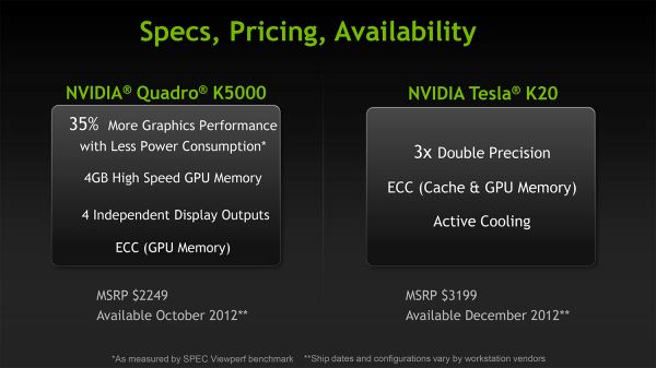
K20 Pricing As Announced During Quadro K5000 Launch
As for the total number of cards they’re looking at shipping and the breakdown of K20/K20X, NVIDIA’s professional solutions group is as mum as usual, but whatever it is we’re being told it won’t initially be enough. NVIDIA is already taking pre-orders through their server partners, with a very large number of pre-orders outstripping the supply of cards and creating a backlog.
Interestingly NVIDIA tells us that their yields are terrific – a statement backed up in their latest financial statement – so the problem NVIDIA is facing appears to be demand and allocation rather than manufacturing. This isn’t necessarily a good problem to have as either situation involves NVIDIA selling fewer Teslas than they’d like, but it’s the better of the two scenarios. Similarly, for the last month NVIDIA has been offering time on a K20 cluster to customers, only for it to end up being oversubscribed due to the high demand from customers. So NVIDIA has no shortage of customers at the moment.
Ultimately the Tesla K20 launch appears to be shaping up very well for NVIDIA. Fermi was NVIDIA’s first “modern” compute architecture, and while it didn’t drive the kind of exponential growth that NVIDIA had once predicted it was very well received regardless. Though there’s no guarantee that Tesla K20 will finally hit that billion dollar mark, the K20 enthusiasm coming out of NVIDIA is significant, legitimate, and infectious. Powering the #1 computer in the Top500 list is a critical milestone for the company’s Tesla business and is just about the most positive press the company could ever hope for. With Titan behind them, Tesla K20 may be just what the company needs to finally vault themselves into a position as a premiere supplier of HPC processors.
GK110: The GPU Behind Tesla K20
Now that we’ve discussed the Telsa K20 series from the big-picture perspective of performance, configurations, pricing, and the marketplace, we can finally dive into the technical underpinnings of the K20.
Announced alongside the Tesla K20 back at NVIDIA’s GTC 2012 was the GPU that would be powering it: GK110. In a reversal of their usual pattern, GK110 was to be NVIDIA’s first compute-oriented Kepler GPU (GK10X having been significantly stripped for gaming efficiency purposes), but it would be the last Kepler GPU to launch. Whereas in the Fermi generation we saw GF100 first and could draw some conclusions about the eventual Tesla cards from that, GK110 has been a true blank slate. On the other hand because it builds upon NVIDIA’s earlier Kepler GPUs, we can draw a clear progression from GK104 to GK110.
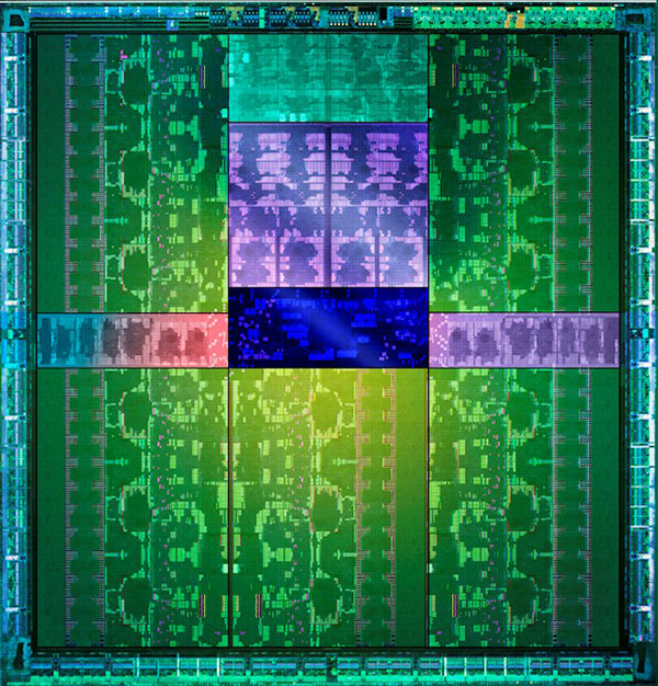
GK110 is NVIDIA’s obligatory big-die GPU. We don’t have a specific die size, but at 7.1 billion transistors it is now the biggest GPU ever built in terms of transistors, dwarfing the 3.5B transistor GK104 and the 4.3B transistor Tahiti GPU from AMD. These big-die GPUs are unwieldy from a fabrication and power consumption perspective, but the end result is that the performance per GPU is unrivaled due to the fact that so many tasks (both graphical and compute) are embarrassingly parallel and map well to the large arrays of streaming processors found in a GPU.
Like GF100 before it, GK110 has been built to fill multiple roles. For today’s launch we’re mostly talking about it from a compute perspective – and indeed most of the die is tied up compute hardware – but it also has all of the graphics hardware we would expect in an NVIDIA GPU. Altogether it packs 15 SMXes and 6 ROP/L2/memory controller blocks, versus 8 SMXes and 4 ROP/L2/memory blocks on GK104. Not accounting for clockspeeds this gives GK110 87% more compute performance and 50% more memory bandwidth than GK104. But there’s a great deal more to GK110 than just a much larger collection of functional units.
| NVIDIA GPU Comparison | ||||||
| Fermi GF100 | Fermi GF104 | Kepler GK104 | Kepler GK110 | |||
| Compute Capability | 2.0 | 2.1 | 3.0 | 3.5 | ||
| Threads/Warp | 32 | 32 | 32 | 32 | ||
| Max Warps/SM(X) | 48 | 48 | 64 | 64 | ||
| Max Threads/SM(X) | 1536 | 1536 | 2048 | 2048 | ||
| Register File | 32,768 | 32,768 | 65,536 | 65,536 | ||
| Max Registers/Thread | 63 | 63 | 63 | 255 | ||
| Shared Mem Config |
16K 48K |
16K 48K |
16K 32K 48K |
16K 32K 48K |
||
| Hyper-Q | No | No | No | Yes | ||
| Dynamic Parallelism | No | No | No | Yes | ||
Fundamentally GK110 is a highly enhanced if not equally specialized version of the Kepler architecture. The SMX, first introduced with GK104, is the basis of GK110. Each GK104 SMX contained 192 FP32 CUDA cores, 8 FP64 CUDA cores, 256KB of register file space, 64KB of L1 cache, 48KB of uniform cache. In turn it was fed by 4 warp schedulers, each with two dispatch units, allowing GK104 to issue instructions from warps in a superscalar manner.
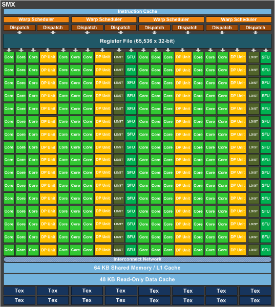
GK110 SMX
GK110 builds on that by keeping the same general design, but tweaking it for GK110’s compute-focused needs. The single biggest change here is that rather than 8 FP64 CUDA cores GK110 has 64 FP64 CUDA cores, giving it 8 times the FP64 performance of a GK104 SMX. The SMXes are otherwise very similar at a high level, featuring the same 256KB of register file space, 64KB of L1 cache, 48KB of uniform cache, and the same warp scheduler structure. This of course does not include a number of low level changes that further set apart GK104 and GK110.
Meanwhile this comparison gets much more jarring if we take a look at GK110 versus GF100 and by extension Tesla K20 versus its direct predecessors, the Fermi based Tesla family. The GK110 SMX compared to the GF100 SM is nothing short of a massive change. Superficially NVIDIA has packed many more CUDA cores into an SMX than they have an SM due to the change from a shader design that ran fewer CUDA cores at a very high (double pumped) clockspeed to a design that runs many more CUDA cores at a lower (single pumped) clockspeed, but they also have changed their warp execution model on its head in the process.
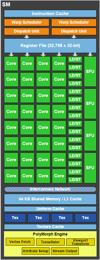
GF100/GF110 SM
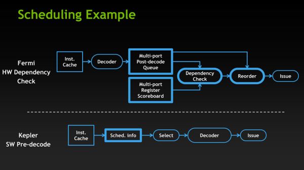
GF100 was essentially a thread level parallelism design, with each SM executing a single instruction from up to two warps. At the same time certain math instructions had variable latencies, so GF100 utilized a complex hardware scoreboard to do the necessary scheduling. Compared to that, GK110 introduces instruction level parallelism to the mix, making the GPU reliant on a mix of high TLP and high ILP to achieve maximum performance. The GPU now executes from 4 warps, ultimately executing up to 8 instructions at once if all of the warps have ILP-suitable instructions waiting. At the same time scheduling has been moved from hardware to software, with NVIDIA’s compiler now statically scheduling warps thanks to the fact that every math instruction now has a fixed latency. Finally, to further improve SMX utilization FP64 instructions can now be paired with other instructions, whereas on GF100 they had to be done on their own.
The end result is that at an execution level NVIDIA has sacrificed some of GF100’s performance consistency by introducing superscalar execution – and ultimately becoming reliant on it for maximum performance. At the same time they have introduced a new type of consistency (and removed a level of complexity) by moving to fixed latency instructions and a static scheduled compiler. Thankfully a ton of these details are abstracted from programmers and handled by NVIDIA’s compiler, but for HPC users who are used to getting their hands dirty with low level code they are going to find that GK110 is more different than it would seem at first glance.
With that said, even with the significant changes to their warp execution model, GK110 brings more changes yet. We can’t hope to replicate the sheer amount of depth NVIDIA’s own GK110 whitepaper covers, but there are several other low-level changes that further separate GK110 from GF100.
Space and bandwidth for both the register file and the L2 cache have been greatly increased for GK110. At the SMX level GK110 has 256KB of register file space, composed of 65K 32bit registers, as compared to 128KB of such space (32K registers) on GF100. Bandwidth to those register files has in turn been doubled, allowing GK110 to read from those register files faster than ever before. As for the L2 cache, it has received a very similar treatment. GK110 uses an L2 cache up to 1.5MB, twice as big as GF110; and that L2 cache bandwidth has also been doubled.
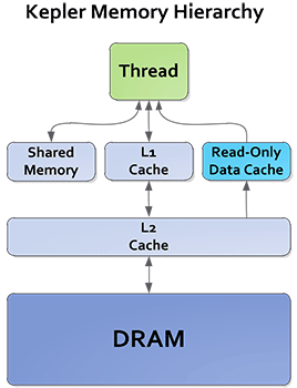
What makes this all the more interesting is that while NVIDIA significantly increased the number of CUDA cores in an SM(X), in fact by far more than the increase in cache and register file sizes, they only marginally increased the number of threads that are actually active on an SMX. Each GK110 SMX can only have up to 2K threads at any time, 1.33x that of GF100 and its 1.5K threads. So as a result GK110 is working from a thread pool only slightly larger than what GF100 worked with, which means that despite the increase in CUDA cores they actually improve their performance in register-starved scenarios as there are more registers available to each thread. This goes hand in hand with an increase in the total number of registers each thread can address, moving from 63 registers per thread on GF100 to 255 registers per thread with GK110.
While we’re on the subject of caches, it’s also worth noting that NVIDIA has reworked their texture cache to be more useful for compute. On GF100 the 12KB texture cache was just that, a texture cache, only available to the texture units. As it turns out, clever programmers were using the texture cache as another data cache by mapping normal data at texture data, so NVIDIA has promoted the texture cache to a larger, more capable cache on GK110. Now measuring 48KB in size, in compute mode the texture cache becomes a read-only cache, specializing in unaligned memory access patterns. Furthermore error detection capabilities have been added to it to make it safer for use with workloads that rely on ECC.
Last, but certainly not least in our low level look, NVIDIA has added a number of new instructions and operations to GK110 to further improve performance. New shuffle instructions allow for threads within a warp to share (i.e. shuffle) data without going to shared memory, making the process much faster than the old load/share/store method. Meanwhile atomic operations have also been overhauled, with NVIDIA both speeding up the execution speed of atomic operations and adding some FP64 operations that were previously only available for FP32 data.
Efficiency Through Hyper-Q, Dynamic Parallelism, & More
When NVIDIA first announced K20 they stated that their goal was to offer 3x the performance per watt of their Fermi based Tesla solutions. With wattage being held nearly constant from Fermi to Kepler, NVIDIA essentially needed to triple their total performance to reach that number.
However as we’ve already seen from NVIDIA’s hardware specifications, K20 triples their theoretical FP32 performance but not their theoretical FP64 performance, due to the fact that NVIDIA’s FP64 execution rate falls from ½ to 1/3their FP32 rate. Does that mean NVIDIA has given up on tripling their performance? No, but with Kepler the solution isn’t just going to be raw hardware, but the efficient use of existing hardware.
Of everything Kepler and GK110 in particular add to NVIDIA’s compute capabilities, their marquee features, HyperQ and Dynamic Parallelism, are firmly rooted in maximizing their efficiency. Now that we’ve seen what NVIDIA’s hardware can do at a low level, we’ll wrap up our look at K20 and GK110 by looking at how NVIDIA intends to maximize their efficiency and best feed the beast that is GK110.
Hyper-Q
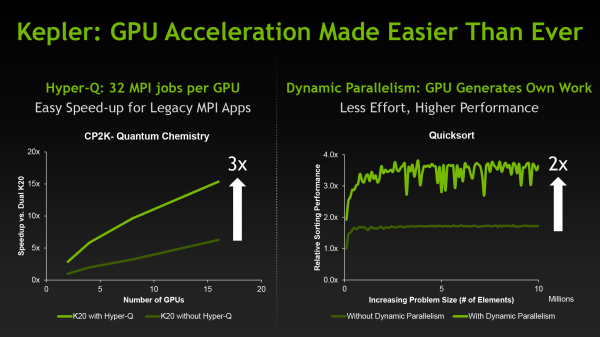
Sometimes the simplest things can be the most powerful things, and this is very much the case for Hyper-Q. Simply put, Hyper-Q expands the number of hardware work queues from 1 on GF100 to 32 on GK110. The significance of this being that having 1 work queue meant that GF100 could be under occupied at times (that is, hardware units were left without work to do) if there wasn’t enough work in that queue to fill every SM or if there were dependency issues, even with parallel kernels in play. By having 32 work queues to select from, GK110 can in many circumstances achieve higher utilization by being able to put different program streams on what would otherwise be an idle SMX.
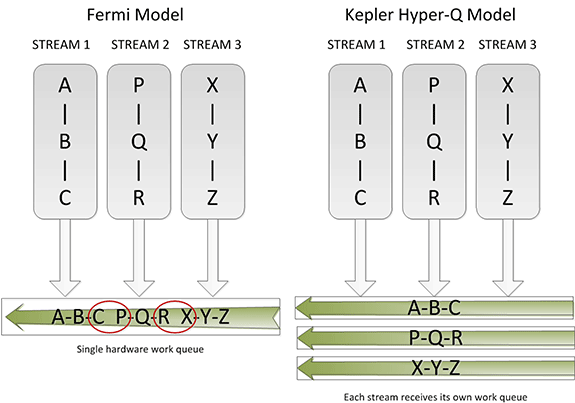
The simplistic nature of Hyper-Q is further reinforced by the fact that it’s designed to easily map to MPI, a common message passing interface frequently used in HPC. As NVIDIA succinctly puts it, legacy MPI-based algorithms that were originally designed for multi-CPU systems and that became bottlenecked by false dependencies now have a solution. By increasing the number of MPI jobs (a very easy modification) it’s possible to utilize Hyper-Q on these algorithms to improve the efficiency all without changing the core algorithm itself. Ultimately this is also one of the ways NVIDIA hopes to improve their HPC market share, as by tweaking their hardware to better map to existing HPC workloads is in this fashion NVIDIA’s hardware will become a much higher performing option.
Dynamic Parallelism
If Hyper-Q was the simple efficiency feature, then NVIDIA’s other marquee feature, Dynamic Parallelism, is the harder and more complex of the features.
Dynamic Parallelism is NVIDIA’s name for the ability for kernels to be able to dispatch other kernels. With Fermi only the CPU could dispatch a new kernel, which incurs a certain amount of overhead by having to communicate back and forth with the CPU. By giving kernels the ability to dispatch their own child kernels, GK110 can both save time by not having to go back to the GPU, and in the process free up the CPU to work on other tasks.
The difficult of course comes from the fact that dynamic parallelism implicitly relies on recursion, to which as the saying goes “to understand recursion, you must first understand recursion”. The use of recursion brings with it many benefits so the usefulness of dynamic parallelism should not be understated, but if nothing else it’s a forward looking feature. Recursion isn’t something that can easily be added to existing algorithms, so taking full advantage of dynamic parallelism will require new algorithms specifically designed around it. (ed: fork bombs are ready-made for this)
Reduced ECC Overhead
Although this isn’t strictly a feature, one final efficiency minded addition to GK110 is the use of a new lower-overhead ECC algorithm. As you may recall, Tesla GPUs implement DRAM ECC in software, allowing ECC to be added without requiring wider DRAM busses to account for the checkbits, and allowing for ECC to be enabled and disabled as necessary. The tradeoff for this is that enabling ECC consumes some memory bandwidth, reducing effective memory bandwidth to kernels running on the GPU. GK110 doesn’t significantly change this model, but what it does do is reduce the amount of ECC checkbit traffic that results from ECC being turned on. The amount of memory bandwidth saved is workload dependent, but NVIDIA’s own tests are showing that the performance hit from enabling ECC has been reduced by 66% for their internal test suite.
Putting It All Together: The Programmer
Bringing things to a close, while we were on the subject of efficiency the issue of coder efficiency came up in our discussions with NVIDIA. GK110 is in many ways a direct continuation of Fermi, but at the same time it brings about a significant number of changes. Given the fact that HPC is so performance-centric and consequently often so heavily tuned for specific processors (a problem that also spans to consumer GPGPU workloads) we asked NVIDIA about just how well existing programs run on K20.
The short answer is that despite the architectural changes between Fermi and GK110, existing programs run well on K20 and are usually capable of taking advantage of the additional performance offered by the hardware. It’s clear that peak performance on K20 will typically require some rework, particularly to take advantage of features like dynamic parallelism, but otherwise we haven’t been hearing about any notable issues transitioning to K20 thus far.
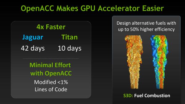
Meanwhile as part of their marketing plank NVIDIA is also going to be focusing on bringing over additional HPC users by leveraging their support for OpenACC, MPI, and other common HPC libraries and technologies, and showcasing just how easy porting HPC programs to K20 is when using those technologies. Note that these comparisons can be a bit misleading since the core algorithms of most programs are complex yet code dense, but the main idea is not lost. For NVIDIA to continue to grow their HPC market share they will need to covert more HPC users from other systems, which means they need to make it as easy as possible to accommodate their existing code and tools.

