Original Link: https://www.anandtech.com/show/5685/apple-a5x-die-size-measured-16294mm2-likely-still-45nm
Apple A5X Die Size Measured: 162.94mm^2, Samsung 45nm LP Confirmed
by Anand Lal Shimpi on March 16, 2012 1:59 PM EST

Contrary to what we thought yesterday based on visual estimation of the A5X die, Chipworks has (presumably) measured the actual die itself: 162.94mm^2. While the A5 was big, this is absolutely huge for a mobile SoC. The table below puts it in perspective.
| CPU Specification Comparison | ||||||||
| CPU | Manufacturing Process | Cores | Transistor Count | Die Size | ||||
| Apple A5X | 45nm? | 2 | ? | 163mm2 | ||||
| Apple A5 | 45nm | 2 | ? | 122mm2 | ||||
| Intel Sandy Bridge 4C | 32nm | 4 | 995M | 216mm2 | ||||
| Intel Sandy Bridge 2C (GT1) | 32nm | 2 | 504M | 131mm2 | ||||
| Intel Sandy Bridge 2C (GT2) | 32nm | 2 | 624M | 149mm2 | ||||
| NVIDIA Tegra 3 | 40nm | 4+1 | ? | ~80mm2 | ||||
| NVIDIA Tegra 2 | 40nm | 2 | ? | 49mm2 | ||||
The PowerVR SGX 543MP2 in Apple's A5 takes up just under 30% of the SoC's 122mm^2 die size, or around 36.6mm^2 just for the GPU. Double the number of GPU cores as Apple did with the A5X and you're looking at a final die size of around 160mm^2, which is exactly what Chipworks came up with in their measurement.
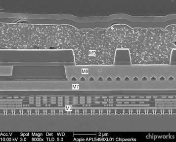
Update: Chipworks confirmed the A5X is still built on Samsung's 45nm LP process. You can see a cross-section of the silicon above. According to Chipworks' analysis, the A5X features 9 metal layers.
Note that this is around 2x the size of NVIDIA's Tegra 3. It's no surprise Apple's GPU is faster, it's spending a lot more money than NVIDIA to deliver that performance. From what I hear, NVIDIA's Wayne SoC will finally show what the GPU company is made of. The only issue is that when Wayne shows up, a Rogue based A6 is fairly likely. The mobile GPU wars are going to get very exciting in 2013.
Image Courtesy iFixit
Thanks to @anexanhume for the tip!


